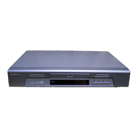
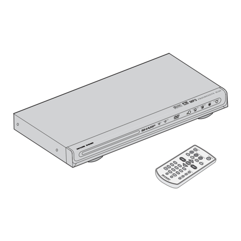
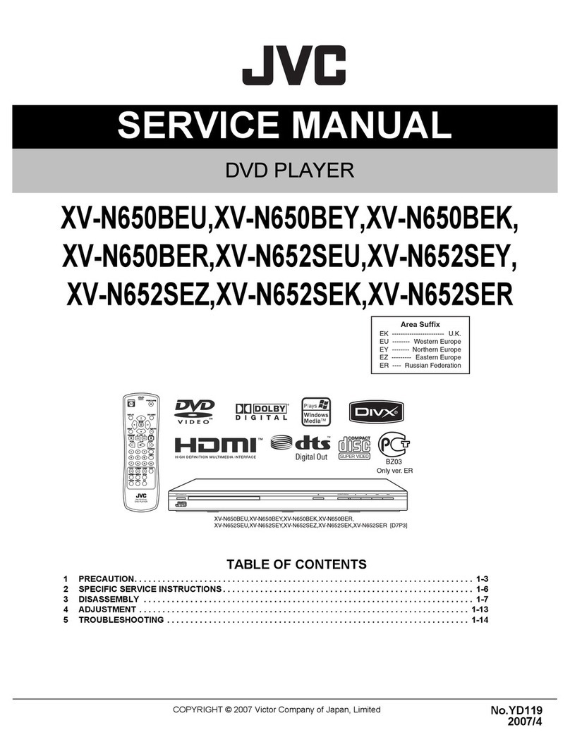
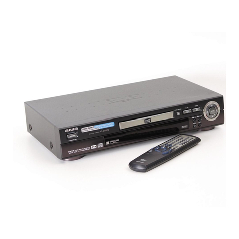
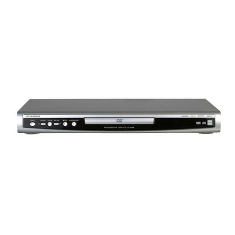
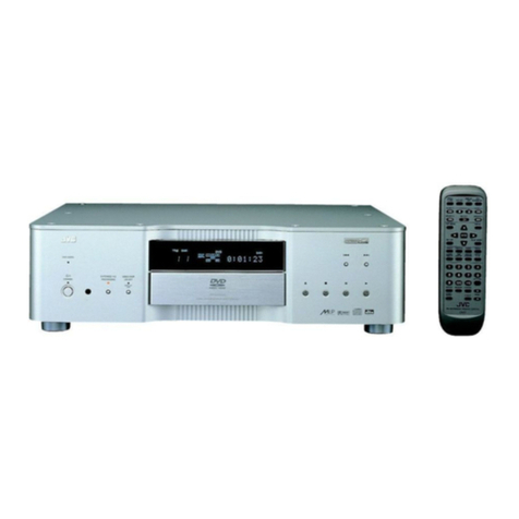
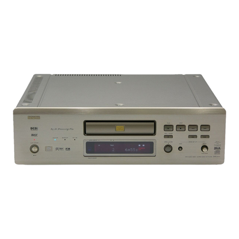
DV-760X
2. FEATURES
2-1
• Plays DVD, video CD and CD (Digital Audio) discs
• Built-in Dolby Digital decoder supporting Dolby Pro Logic*1 decoding and Virtual Surround
• For the audio on a DVD disc recorded in MPEG Audio Version 2.0 multi channel (5.1ch)
• New Digital Gamma correction and New Digital Super Picture functions
• Separate colour component output connectors (Y, PB(CB) and PR(CR))
• DTS*2 AUDIO DECODER (DIGITAL THEATRE SYSTEM)
*1Manufactured under license from Dolby Laboratories. "Dolby", "Pro Logic" and the double-D symbol are trademarks of
Dolby Laboratories.
*2 "DTS" and "DTS Digital Surround" are trademarks of Digital Theater Systems, Inc.
3. SPECIFICATIONS
Signal System: NTSC/PAL
Video output: Output connector: Pin-jack
Output level: 1 Vp-p (75Ω)
S video output: Y output level: 1 Vp-p (75Ω)
C output level: 0.30 Vp-p (75Ω)
Output connector: S connector
Component colour output: Y output level: 1 Vp-p (75Ω)
PB(CB) output level: 0.525 Vp-p (75Ω)/75% colour
PR(CR) output level: 0.525 Vp-p (75Ω)/75% colour
Output connector: Pin-jack
Audio output: 5.1ch output: Front L/R, surround L/R, centre and subwoofer
5ch output: Front L/R, surround L/R and center
Output connector: Pin-jack
Output level: 2 Vrms (1 kHz, 0 dB)
Digital audio I/F: Optical digital output: Optical connector
Audio output: Coaxial digital output: Pin-jack
Headphone output: Output connector: Standard jack
Video signal horizontal resolution: 500 lines (DVD)
S/N ratio: 60 dB (DVD)
Audio signal frequency characteristics: For DVD linear PCM playback:
4 Hz to 22 kHz (48 kHz sampling)
4 Hz to 44 kHz (96 kHz sampling)
CD playback: 4Hz to 20 kHz (EIAJ)
(MPEG Audio 1/2)
S/N ratio: CD: 105 dB, 1 kHz (EIAJ)
Dynamic range: DVD linear PCM: 94 dB (EIAJ)
CD: 94 dB (EIAJ)
Total harmonic distortion ratio: CD: 0.005% or less (EIAJ)
Operating temperature: 5°C to 40°C
Storage temperature: –20°C to 55°C
Power supply : 220 V to 240 V AC, 50/60 Hz
Power consumption: 16 W
Dimensions: 430 mm × 351 mm × 97 mm (W × D× H) (Including attachments)
Weight: 3.8 kg
Specifications are subject to change without notice.
Weight and dimensions are approximate.
Digital Output
·Thedigitaloutputformat(opticalorcoaxial)usedinthisDVDplayerislinearPCMaudiosamplingat44.1kHz or 48 kHz.
Linear PCM sound for DVD video discs sampled at 96 kHz cannot be output digitally.
Check the disc jacket for information on the audio sampling used.
3-1. ACCESSORIES
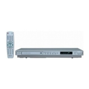
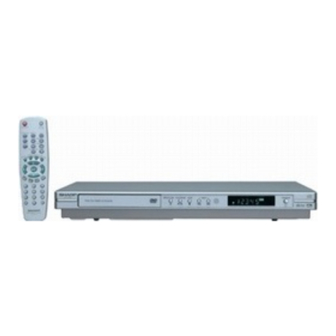
Accessories: Video/audio cord x 1, UM3 battery x 2,
Remote Control Unit x 1, S-Video cord x 1
