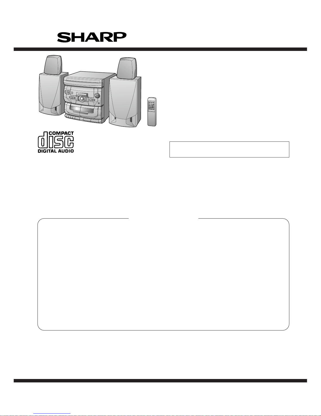
Sharp CD-C602 User manual

CD-C602,CP-C602
– 1 –
CD-C602
CP-C602
• In the interests of user-safety the set should be restored to its
original condition and only parts identical to those specified be
used.
SERVICE MANUAL
SHARP CORPORATION
No. S1903CDC602//
This document has been published to be used
for after sales service only.
The contents are subject to change without notice.
CONTENTS Page
IMPORTANT SERVICE NOTES (FOR U.S.A. ONLY)....................................................................................................... 2
SPECIFICATIONS ............................................................................................................................................................. 2
NAMES OF PARTS ........................................................................................................................................................... 3
QUICK GUIDE ................................................................................................................................................................... 5
DISASSEMBLY.................................................................................................................................................................. 6
REMOVING AND REINSTALLING THE MAIN PARTS..................................................................................................... 8
ADJUSTMENT ................................................................................................................................................................... 9
NOTES ON SCHEMATIC DIAGRAM .............................................................................................................................. 11
TYPE OF TRANSISTER.................................................................................................................................................. 11
WAVEFORMS OF CD CIRCUIT...................................................................................................................................... 12
BLOCK DIAGRAM ........................................................................................................................................................... 13
SCHEMATIC DIAGRAM / WIRING SIDE OF P.W.BOARD..............................................................................................16
VOLTAGE ........................................................................................................................................................................ 28
TROUBLESHOOTING ..................................................................................................................................................... 29
FUNCTION TABLE OF IC................................................................................................................................................ 33
LCD SEGMENT ................................................................................................................................................................38
PARTS GUIDE/EXPLODED VIEW
PACKING OF THE SET (FOR U.S.A. ONLY)
CD-C602 mini component system consisting of
CD-C602 mini component system, CP-C602 and rear
(GBOXS0020AWM1) speaker system.

CD-C602,CP-C602
– 2 –
FOR A COMPLETE DESCRIPTION OF THE OPERATION OF THIS UNIT, PLEASE REFER
TO THE OPERATION MANUAL.
CD-C602 CP-C602
IMPORTANT SERVICE NOTES (FOR U.S.A. ONLY)
BEFORE RETURNING THE AUDIO PRODUCT
(Fire & Shock Hazard)
Before returning the audio product to the user, perform the
following safety checks.
1. Inspect all lead dress to make certain that leads are not
pinchedorthathardwareisnotlodgedbetweenthechassis
and other metal parts in the audio product.
2. Inspect all protective devices such as insulating materials,
cabinet, terminal board, adjustment and compartment
covers or shields, mechanical insulators etc.
3. To be sure that no shock hazard exists, check for leakage
current in the following manner.
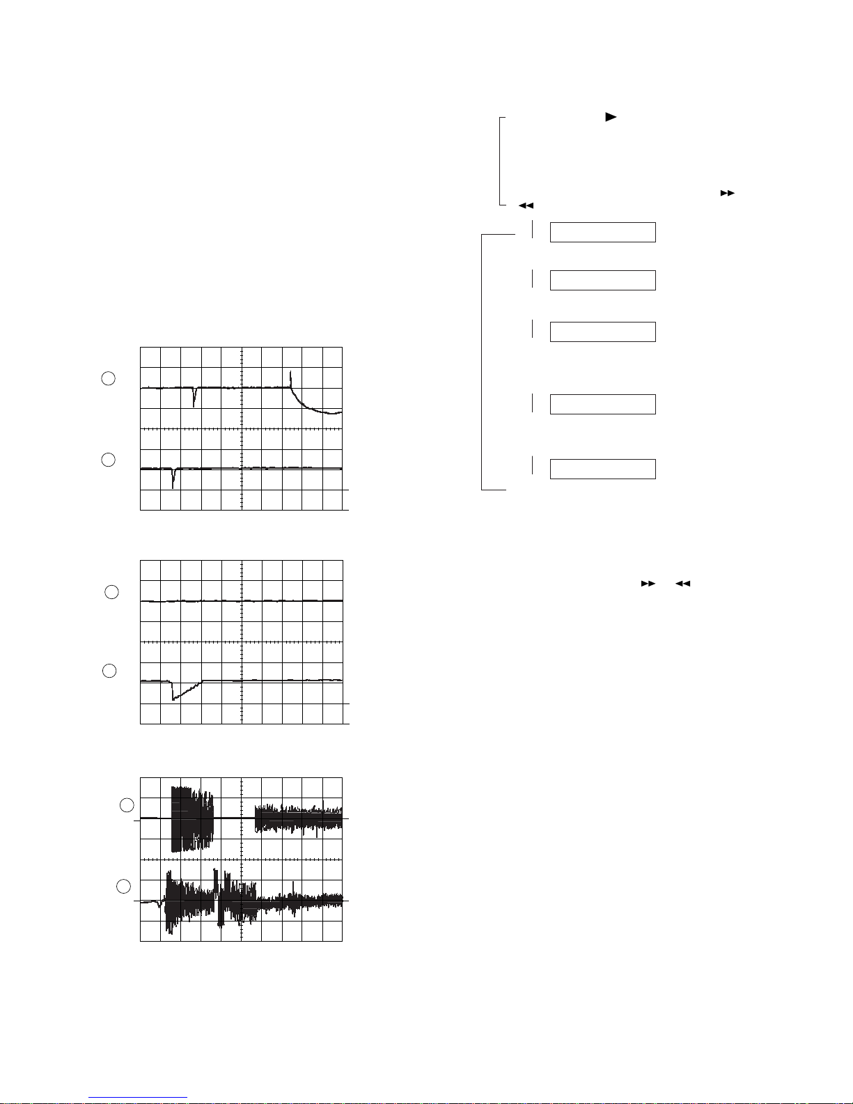
* Plug the AC line cord directly into a 120 volt AC outlet.
* Using two clip leads, connect a 1.5k ohm, 10 watt resistor
paralleled by a 0.15µF capacitor in series with all exposed
metal cabinet parts and a known earth ground, such as
conduit or electrical ground connected to earth ground.
* Use a VTVM or VOM with 1000 ohm per volt, or higher,
sensitivity to measure the AC voltage drop across the
resistor (See diagram).
* Connect the resistor connection to all exposed metal parts
havingareturnpathtothechassis(antenna,metalcabinet,
screw heads, knobs and control shafts, escutcheon, etc.)
and measure the AC voltage drop across the resistor.
AllcheckmustberepeatedwiththeAClinecordplugconnection
reversed.
Anyreading of0.3volt RMS(thiscorrespondsto0.2 milliamp.
AC.) or more is excessive and indicates a potential shock
hazard which must be corrected before returning the audio
product to the owner.
SPECIFICATIONS
Specifications for this model are subject to change without prior
notice.
AC SCALE
VTVM
1.5k ohms
10W
0.15µF
TEST PROBE
TO EXPOSED
METAL PARTS
CONNECT TO
KNOWN EARTH
GROUND
GBOXS0020AWM1
General
Power source: AC 120 V, 60 Hz
Power consumption: 25 W
Dimensions: Width; 10-5/8" (270 mm)
Height; 11-1/16" (280 mm)
Depth; 13-1/8" (332.5 mm)
Weight: 9.2 lbs. (4.2 kg)
Amplifier section
Output terminals: Headphones; 16-50 ohms
(recommended; 32 ohms)
Front speaker ; 6 ohms
Rear speaker ; 12 ohms
Tuner section
Frequency range: FM; 87.5-108 MHz
AM; 530-1,720 kHz
Cassette deck section
Frequency response:50-14,000 Hz (Normal tape)
Signal/noise ratio: 50 dB (TAPE 1, recording/playback)
55 dB (TAPE 2, playback)
Wow and flutter: 0.15 % (WRMS)
Compact disc player section
Type: 3-disc multi-play compact disc player
Signal readout: Non-contact,3-beam semiconductor
laser pickup
D/A converter: 1-bit D/A converter
Frequency response:20 -20,000 Hz
Dynamic range: 90 dB (1 kHz)
Front speaker section
Type: 4" (10 cm) full-range speaker
Maximum input
power: 5 W
Impedance: 6 ohms
Dimensions: Width; 6-11/16" (170 mm)
Height; 11-1/16" (280 mm)
Depth; 5-15/16" (151 mm)
Weight: 3.1 lbs. (1.4 kg)/each
Rear speaker section
Type: 3-3/32" (8 cm) full-range speaker
Maximum input
power: 4 W
Impedance: 12 ohms
Dimensions: Width; 6" (150 mm)
Height; 6" (150 mm)
Depth; 3" (78 mm)
Weight: 0.9 lbs. (0.4 kg)/each
●
●
●
●
●
●
●

CD-C602,CP-C602
– 3 –
NAMES OF PARTS
CD-C602
■Front panel
11.
Disc Tray
12.
CD Play Indicator:
13.
Disc Number Indicators
14.
FM Stereo Mode Indicator: ST
15.
Extra Bass Indicator: X-BASS
16.
Memory Indicator
17.
CD Pause Indicator:
18.
CD Repeat Indicator:
19.
FM Stereo Indicator:
10.
Power Button
11.
Memory Button
12.
Extra Bass Button: X-BASS
13.
Volume Up/Down Buttons: /
14.
Function Selector Button
15.
Band Selector Button
16.
Tuning Up/Down Buttons: /
17.
(CD) Track Down/Review Button: /
3
(TUNER) Preset Down Button:
18.
Stop Button:
19.
Play/Repeat Button: /
20.
(CD) Track Up/Cue Button: /
3
(TUNER) Preset Up Button:
21.
Disc Skip Button
22.
Open/Close Button:
23.
Headphone Socket
24.
(TAPE 1) Cassette Compartment
25.
(TAPE 2) Cassette Compartment
26.
(TAPE 1) Record Button:
27.
(TAPE 1) Play Button:
28.
(TAPE 1) Rewind Button:
29.
(TAPE 1) Fast Forward Button:
30.
(TAPE 1) Stop/Eject Button: /
31.
(TAPE 2) Play Button:
32.
(TAPE 2) Stop/Eject Button: /
■Rear panel
11.
AC Power Input Socket
12.
Speaker Terminals
13.
FM/AM Loop Aerial Socket
1
ST
X-BASS
MEMORY
123
23 4 6
8
5
7
9
10 11 12 13
14
15
16 17 18 19 20 21 22 23
24 25
2627282930 31 32
3
1
2

CD-C602,CP-C602
– 4 –
CP-C602
GBOXS0020AWM1
CD-C602
■Remote control
11.
Remote Control Transmitter LED
12.
Stop Button:
13.
(CD) Track Down/Review Button: /
3
(TUNER) Preset Down Button:
14.
(CD) Track Up/Cue Button: /
3
(TUNER) Preset Up Button:
15.
Play/Repeat Button:
16.
Disc Skip Button
17.
Pause Button:
18.
Memory Button
19.
Clear Button
10.
Extra Bass Button: X-BASS
11.
Function Selector Buttons
12.
Power Button
13.
Volume Up/Down Buttons: /
●Rear speaker
11.
Woofer
12.
Speaker Wire
■Speaker section
●Front speaker
13.
Woofer
14.
Bass Reflex Duct
15.
Speaker Wire
45
3
1
2
3
4
5
6
7
89
10
11
12 13
1
2
RESETTINGTHE MICROCOMPUTER
1
Press the POWER button to turn the power off.
2
Press and hold down the POWER button and the
button at the same time. Hold them down for at least 1
second.
3
Press the POWER button to turn the power on.
Caution:
The operation explained above will erase all data stored
in memory including the tuner and CD presets.
Reset the microcomputer by performing the following
procedure for the cases shown below:
To erase all of the stored memory contents, or
If the display does not function properly, or
The unit does not operate properly.
●
●
●
●
■

CD-C602,CP-C602
– 5 –
2
13
LEFTLEFT
RATED SPEAKER IMPEDANCE:
6 OHMS MIN 12 OHMS MIN .
RIGHTRIGHT
FRONT
SPEAKERS REAR
SPEAKERS
MINI COMPONENT SYSTEM Quick-Guide
CD-C602
Guía rápida
●AC 120 V, 60 Hz
●
120 V de CA, 60 Hz
Remote control
Control remoto
Remote Sensor
Sensor remote
●2 “AA” batteries
●
Dos pilas “AA”
●Batteries are not included.
●
Las pilas no están incluidas.
Turning the power on and off
Conexión y desconexión de la
alimentación
Preparation for use
Preparación para su uso
POWER
POWER
15
15
8" - 20' (0.2m - 6m)
0,2m - 6m
CD playback
Reproducción de discos compactos
●“Cd” will appear in
the display
●
“Cd” aparecerá en
el visualizador
●Label facing up
●
Etiqueta hacia arriba
FUNCTION OPEN
/CLOSE OPEN
/CLOSE
(Right)
(Derecho)
(Left)
(Izquierdo)
(Right)
(Derecho)
(Left)
(Izquierdo)
●AM Loop Antenna
●
Antena de cuadro
de AM
●FM Antenna
●
Antena de FM
Black
Negro
Red
Rojo
Black
Negro
Red
Rojo
Wire with the white line
Cable con la línea blanca
Recording from CDs
Grabación de discos compactos
●“Cd” will appear in
the display
●
“Cd” aparecerá en
el visualizador
●Load the disc to be
recorded.
●
Introduzca el disco
que va a grabar.
●CD recording starts.
●
La grabación de CD
empieza.
Tape playback
Reproducción de cintas
Radio operation
Funcionamiento de la radio
Sound control
Control del sonido
TAPE 1 TAPE 2
PLAY STOP/EJECT
/
STOP/EJECT
/
FUNCTION
●“Tape” will appear
in the display
●
“Tape” aparecerá
en el visualizador
●“Tuner” will appear
in the display
●
“Tuner” aparecerá
en el visualizador
TINSZ0394AWZZ
●Volume
●
Volumen
●Extra-BASS
●
Graves extra
Printed in Malaysia
Impreso en Malaysia
VOLUME
X-BASS
VOLUME
UP
DOWN
X-BASS
VOLUME
UP
DOWN
X-BASS
●The sound level at a given volume setting depends
on a combination of speaker efficiency, location
and many other factors. It is advisable to avoid
exposure to high volume levels, which occur while
turning the unit on with the volume control setting
up high, or while continually listening at high
volume levels.
●
El nivel de sonido en una posición de volumen
fijado depende de una combinación del
rendimiento de las altavoces, la posición y muchos
otros factores.Es aconsejable evitar un aumento
de volumen.Esto se produce, por ejemplo, al
conectar el aparato con el volumen puesto en una
posición alta.Evite continuar la audición
prolongada a altos niveles de sonido.
●Only discs bearing the logo as shown can be
played in this unit.
●
En este aparato sólo pueden reproducirse los
discos que tengan el logotipo mostrado.
Precaution
Precaucíon
FUNCTION
TAPE 1
RECORD
STOP/EJECT
/
STOP/EJECT
/
A9812.HK
FUNCTION TUNING TUNING
BAND
ST
MHz
kHz
MHz
FM STEREO
FM MONO
AM
QUICK GUIDE

CD-C602,CP-C602
– 6 –
DISASSEMBLY
Caution on Disassembly
Follow the below-mentioned notes when disassembling
the unit and reassembling it, to keep it safe and ensure
excellent performance:
1. Take cassette tape and compact disc out of the unit.
2. Be sure to remove the power supply plug from the wall
outlet before starting to disassemble the unit.
3.Takeoffnylonbandsor wire holders where they need to
beremovedwhendisassemblingtheunit.Afterservicing
theunit,besuretorearrange the leads where they were
before disassembling.
4. Take sufficient care on static electricity of integrated
circuits and other circuits when servicing.
Figure 6-2
1 Top Cabinet 1. Screw ..................... (A1) x4 6-1
2. Hook....................... (A2) x3
2 Side Panel 1. Screw ..................... (B1) x4 6-1
(Left/Right) 2. Screw ..................... (B2) x2
3. Hook....................... (B3) x2
3 CD Tray Cover/ 1. Turn on the power supply, 6-2
CD Player Unit open the disc tray, take out
the CD tray cover, and close.
(Note 1)
2. Hook....................... (C1) x3
3. Hook....................... (C2) x2
4. Socket .................... (C3) x4
4 Back Board 1. Screw ..................... (D1) x3 6-2
5 Main PWB/ 1. Screw ..................... (E1) x10 7-1
Display PWB 2. Hook....................... (E2) x2
3. Socket .................... (E3) x6
6 Front Panel 1. Screw ..................... (F1) x2 7-1
2. Hook....................... (F2) x5
7 Tape Mechanism 1. Open the cassette holder. 7-2
2. Screw...................... (G1) x6
8 Turntable 1. Screw ..................... (H1) x1 7-3
2. Stabilizer ................ (H2) x1
9 Disc Tray 1. Screw ..................... (J1) x2 7-3
2. Guide ..................... (J2) x2
10 CD Changer 1. Screw ..................... (K1) x4 7-4
Mechanism
11 CD Mechanism 1. Screw ..................... (L1) x1 7-4
STEP REMOVAL PROCEDURE FIGURE
Figure 6-1
CD-C602
Figure 6-3
CD-C602
Top Cabinet
(A1)x2
ø3x12mm
(A1)x2
ø3x12mm
(B2)x1
ø3x12mm
(B2)x1
ø3x12mm
(B1)x2
ø3x12mm
Hook
(B3x1)
Hook
(B3x1)
Side Panel
(Left)
Side Panel
(Right)
Back Board
Front Panel
(B1)x2
ø3x12mm
Hook
(A2x3)
Lock Lever
Back Board
CD Player Unit
Hook
Pull
Hook
Pull
(C2)x1
(C2)x1
(C3)x4(D1)x3
ø3x10mm
Front Panel
2
Main PWB
1
Disc Tray
CD Tray Cover
Hook
(C1)x3
1
Note 1:
How to open the change manually.
1. Then, turn fully the lock lever in the arrow direction through
the hole on the loading chassis bottom in this state.
After that, push forward the CD player base. (Fig. 6-3)
2. After removing the connector for the optical pickup fromthe
connector wrap the conductive aluminium foil around the
front end of connector so as to protect the optical pickup
from electrostatic damage.

CD-C602,CP-C602
– 7 –
Figure 7-3
Be careful when installing the CD changer mechanism.
InstalltheCDchangermechanismontheCDplayerbaseafter
the shift lever has been set in the highest position.
Figure 7-4
Figure 7-6
CP-C602
Figure 7-2
Figure 7-1
Figure 7-5
CP-C602
STEP REMOVAL PROCEDURE FIGURE
1 Front Speaker 1. Net ..........................(A1) x1 7-5
2. Duct Panel .............. (A2) x1
3. Screw......................(A3) x4 7-6
Woofer
Speaker Box
(A3) x4
ø4x12mm
Front Panel
Tape
Mechanism
Open
Cassette
Holder
(Left/Right)
(G1)x6
ø3x10mm
Front
Panel
Hook
(E2)x2
Display PWB
Main
PWB
Hook
(F2)x4
(E1)x8
ø3x10mm
(E1)x1
ø3x10mm
(F1)x2
ø3x10mm (E3)x1
(E3)x5
Hook
(F2)x1
PWB
Spacer
PWB Spacer
(E1)x1
ø3x10mm
(K1) x4
ø3 x12mm
(L1) x1
ø2.6 x10mm
CD Changer
Mechanism
CD Mechanism
Shift Lever
CD Player Base
(J1) x1
ø3 x10mm
(J1) x1
ø3 x10mm
(H1) x1
ø3 x10mm
Turntable
Disc Tray
(H2) x1
(J2) x1
(J2) x1
CD Player Unit
Washer
Driver
Driver should be
pried away from
Speaker Box.
Direction of handle
(A1) x1
Speaker Box
(A2) x1

CD-C602,CP-C602
– 8 –
How to remove the turntable up/down/loading
motor (See Fig. 8-1)
1. Remove the screws (A1) x 2 pcs., to remove the turntable
up/down/loading motor.
How to remove the pickup (See Fig. 8-2)
1. Remove the screws (B1) x 2 pcs., to remove the shaft (B2)
x 1 pc.
2. Remove the stop washer (B3) x 1 pc., to remove the gear
(B4) x 1 pc.
3. Remove the pickup.
Figure 8-2
REMOVING AND REINSTALLING THE MAIN PARTS
CD MECHANISM SECTION
Perform steps 1, 2, 3, and 8 ~ 11 of the disassembly method
to remove the CD mechanism.
Figure 8-1
Note:
After disconnecting the optical pickup connector wrap the
front end of connector in conductive aluminum foil so as to
prevent damage to the optical pickup by static electricity.
(B1) x2
(B2) x1
(B3) x1
(B4) x1 CD Mechanism
Pickup
ø2.6 x6mm
(A1) x2
ø2.6 x5mm
Turntable Up/Down/
Loading Motor
Motor
PWB

CD-C602,CP-C602
– 9 –
MECHANISM SECTION
•Driving Force Check
Torque Meter Specified Value
Play: TW-2412 Tape 1: Over 100 g
Tape 2: Over 50 g
•Torque Check
Torque Meter
Tape 2
Play: TW-2111 30 to 60 g. cm 30 to 60 g.cm
Fast forward: TW-2231 80 to 135 g.cm —
Rewind: TW-2231 80 to 135 g.cm —
Specified
Value
Adjusting
Point Instrument
Connection
Test Tape
Normal MTT-111 Volume in 3,000 ±Speaker
speed motor 30 Hz terminal
(Load
resistance:
4 ohms)
ADJUSTMENT
Specified Value
Tape 1
•Tape Speed
• AM IF/RF
Signal generator: 400 Hz, 30%, AM modulated
*1. Input: Antenna (CNP301), Output: TP302
*2. Input: Antenna (CNP301), Output: TP301
TUNER SECTION
fL: Low-range frequency
fH: High-renge frequency
IF 450 kHz 1,720 kHz T351 *1
Band — 530 kHz (fL): T333 *2
Coverage 1.1 ±0.1 V
Tracking 990 kHz 990 kHz (fL): T331 *1
Test Stage Frequency Frequency
Display Setting/
Adjusting
Parts
Instrument
Connection
*1. Input: Antenna (CNP301), Output: TP301
*2. Input: Antenna (CNP301), Output: Speaker terminal
•FM RF
Signal generator: 1 kHz, 22.5 kHz dev., FM modulated
Band — 87.50 MHz L303(fL): *1
Coverage 1.3 V ±0.1 V
RF 98.00 MHz 98.00 MHz L302 *2
(10-30 dB)
Test Stage Instrument
Connection
Frequency Frequency
Display Serring/
Adjusting
Point
•FM Detection
Signal generator: 10.7 MHz, FM sweep generator
Detection 10.7 MHz 98.00 MHz T352 Input: Pin 1 of
IC301
Output: TP302
IF 10.7 MHz 98.00 MHz T301(Turn Input: Pin 1 of
the core of IC301
transformer Output: TP302
T352 fully
counter-
clookwise.)
Instrument
Connection
Test
Stage Adjusting
Parts
Frequency
Display
Frequency
Adjusting
Parts Instrument
Connection
Frequency
Display
Frequency
•VCO Frequency
* Adjust for 76 kHz ±200 Hz.
Notes:
After preparing the test circuit shown in Fig 9-3, connect the
Pin 13 , Pin 21 and ground of the IC351 with test circuit, and
measure the Value.
At this time, apply a standard unmodulated signal input and
adjust the VCO.
Pin 13 of IC351 Pin 21 of IC351
D
G
S
10 kohm
TO FREQUENCY
COUNTER
FET : 2SK19 or 2SK54
Figure 9-3
98.00 MHz 98.00 MHz VR351* Pin 13, Pin 21
(60 dB) and ground
of IC351
TAPE MECHANISM
Volume in motor
Figure 9-2 ADJUSTMENT POINTS
Figure 9-1 ADJUSTMENT POINTS
L303
R319
T331
T301
L301
L302
CNP301
FM/AM
ANTENNA
TERMINAL
T351 T333
IC351
IC301
FM RF
AM Tracking fL
VCO
AM IF
FM IF
VR351
FM Band
Coverage fL
FM Detection
AM Band
Coverage fL
T352
MAIN PWB
1
C360
C364
TP301
+
TP303
TP302
13 21

CD-C602,CP-C602
– 10 –
CD SECTION
Since this CD system incorporates the following automatic
adjustment function, when the pickup is replaced, it is not
necessary to readjust it.
SincethisCDunitdoesnotneedadjustment,thecombination
of PWB and laser pickup unit is not restricted.
• Automatic adjustment item
1. Focus offset (Fig. 10-1)
2. Tracking offset (Fig. 10-2)
3. E/F balance (tracking error balance) (Fig. 10-3)
4. RF level AGC function (HF level: constant)
5. RF level automatic follow-up of the tracking gain
This automatic adjustment is performed each time a disc is
changed.
Therefore,eachdiscisplayedbackusingtheoptimalsettings.
Figure 10-1
Figure 10-2
2
1
10ms
0.50 V
IC1 20 FE
10ms
0.50 V
IC1 7 TE
Enlarged
View
TRACKING
OFF-SET
ADJUST
2
1
TO
TE
200 ms
1V/diV
IC 1 15
200 ms
1V/diV
IC 1 7
TRACKING/
ERROR
BARANCE
ADJUST
Figure 10-3
CDTEST MODE
When the PLAY and POWER buttons are
pressed at the same time in OFF MODE, the
set will enter CD TEST MODE
↓
"CD TEST" of LCD will light up.
↓
The pickup can be moved by using the ( ) or
() button.
↓
LASER ON
↓
FOCUS SERVO ON
↓
TRACKING ON THE STOP
SERVO OFF PLAY
Display "CD 01 0:00"
↓
TRACKING ON THE STOP
SERVO OFF PLAY
↓
STOP "CD TEST" will display
IL is not
performed.
Press PLAY button
Press PLAY button
Press PLAY button
Press PLAY button
Press PLAY button
Cancel method: POWER OFF
LCD display: After the PLAY or APMS MEMORY button has
been pressed, the track No. and time only will
appear (valid).The other items are optional.
Note:The pickup can be slid using the or button only
while in the stop mode.
ALL CLEAR AND RE-START FUNCTION
When the STOP and POWER buttons are pressed to turn on
the power, the entire internal memory will be cleared and the
mechanism will run from address 0.
All of the tuner presets, APMS, TOC and disc numbers which
were last stored in memory will be cleared, and the tuner,
changer mechanism and all of the other items will be initial-
ized.
→
2
0.1s
0.50 V
IC1 20 FE
0.1s
0.50 V
IC1 7 TE
1
FOCUS
OFF-SET
ADJUST
TRACKING
OFF-SET
ADJUST

CD-C602,CP-C602
– 11 –
SW1 OPEN/CLOSE ON—OFF
SW2 MECHA UP ON—OFF
SW3 DISC NUMBER ON—OFF
SW4 PICKUP IN ON—OFF
SW605 TAPE 1 MAIN ON—OFF
SW606 TAPE 2 MAIN ON—OFF
SW607 TAPE 1 RECORD ON—OFF
SW608 TAPE 1 PLAY ON—OFF
SW701 POWER ON—OFF
SW702 VOLUME UP ON—OFF
SW703 VOLUME DOWN ON—OFF
SW704 PLAY ON—OFF
•The indicated voltage in each section is the one measured
by Digital Multimeter between such a section and the chas-
sis with no signal given.
1. In the tuner section,
( ) indicates AM
< > indicates FM stereo
2. In the main section, a tape is being played back.
3. In the deck section, a tape is being played back.
( ) indicates the record state.
4. In the power section, a tape is being played back.
5. In the CD section, the CD is stopped.
•Parts marked with “ ” ( ) are important for
maintaining the safety of the set. Be sure to replace these
parts with specified ones for maintaining the safety and
performance of the set.
NOTES ON SCHEMATIC DIAGRAM
•Resistor:
To differentiate the units of resistors, such symbol as K and
M are used: the symbol K means 1000 ohm and the symbol
M means 1000 kohm and the resistor without any symbol is
ohm-type resistor. Besides, the one with “Fusible” is a fuse
type.
•Capacitor:
To indicate the unit of capacitor, a symbol P is used: this
symbol P means micro-micro-farad and the unit of the
capacitor without such a symbol is microfarad. As to
electrolyticcapacitor,theexpression“capacitance/withstand
voltage” is used.
(CH), (TH), (RH), (UJ): Temperature compensation
(ML): Mylar type
(P.P.): Polypropylene type
•Schematic diagram and Wiring Side of P.W.Board for this
model are subject to change for improvement without prior
notice.
REF. NO DESCRIPTION POSITION POSITION
SW705 FAST FORWARD ON—OFF
SW706 REWIND ON—OFF
SW707 OPEN/CLOSE ON—OFF
SW708 STOP ON—OFF
SW709 DISC SKIP ON—OFF
SW710 X-BASS ON—OFF
SW711 FUNCTION ON—OFF
SW712 BAND ON—OFF
SW714 MEMORY ON—OFF
SW715 TUNING UP ON—OFF
SW716 TUNING DOWN ON—OFF
REF. NO DESCRIPTION
Figure 11 TYPES OF TRANSISTOR
SVC211C
SVC348S
2SC2389 SE
KRA102 M
KRA109 M
KRC102 M
KRC104 M
KTA1266 GR
KTA1271 Y
KTC3194 Y
KTC3199 GR
KTC3203 Y
FRONT
VIEW
E C B
(S)(G)(D)
(1) (2) (3)
2SD2012 Y
FRONT
VIEW
B C E
(D)(G)(S)
(3) (2) (1)
1 2 3

CD-C602,CP-C602
– 12 –
WAVEFORMS OF CD CIRCUIT
1
2
3
REVIEW
0.5ms
1.00 V
IC1 41 HF
0.5ms
5.0 V
IC1 4 HFL
1
3
1
4
0.5ms
5.0 V
IC1 36 TES
1
5
CUE
50ms
10.0 V
IC1 33 JP+
50ms
10.0 V
IC1 32 JP-
1
6
1
7
50ms
0.50 V
IC1 14 JP
1
8
50ms
1.00 V
IC1 7 TE
1
9
0.5ms
10.0 V
IC1 33 JP+
0.5ms
10.0 V
IC1 32 JP-
1
6
1
7
0.5ms
0.50 V
IC1 14 JP
1
8
0.5ms
1.00 V
IC1 7 TE
1
9
REVIEW
50ms
10.0 V
IC1 33 JP+
50ms
10.0 V
IC1 32 JP-
1
6
1
7
50ms
0.50 V
IC1 14 JP
1
8
50ms
1.00 V
IC1 7 TE
1
9
0.5ms
10.0 V
IC1 33 JP+
0.5ms
10.0 V
IC1 32 JP-
1
6
1
7
0.5ms
0.50 V
IC1 14 JP
1
8
0.5ms
1.00 V
IC1 7 TE
1
9
PLAY NORMAL DISC
TN0=01
20ms
1.00 V
IC1 27 SPO
20ms
2.00 V
IC2 12 CLV+
1
10
1
11
PLAY TCD-712 (140mm)
TN0=01
50ms
1.00 V
IC1 27 SPO
50ms
2.00 V
IC2 12 CLV+
1
10
1
11
PLAY TCD-712
1
5s
100mV
IC1 29 SLD
1
12
1
0.5s
100mV
IC1 29 SLD
1
12
3
5ms
0.50 V
IC1 20 FE
1
5ms
5.0 V
IC1 54 DRF
STOP PLAY
FOCUS SERCH
1
1
1
2
1
2
3
CUE
0.5ms
1.00 V
IC1 41 HF
0.5ms
5.0 V
IC1 4 HFL
1
3
1
4
0.5ms
5.0 V
IC1 36 TES
1
5

CD-C602,CP-C602
– 13 –
Figure 13 BLOCK DIAGRAM (1/3)
123467
13 12 24 25 30 31
64
5
62
8
26
29
30
31
54
51
54
3240434449
50
15
16
27
10 12 20 61
9
45
44
6
23
36
53
57
24 28 37 38 39 40 36 41
1
9
37
M
1
5
14
17 20 11 29
22
23
32
26
IC1
LA9241M
SERVO AMP.
IC2
LC78622N
SERVO/SIGNAL
CONTROL
IC5
M56748FP
SL+, SL–, DRF
XIN
XOUT
+B
4.3V
FOCUS
COIL
TRACKING
COIL
M
M
PICKUP UNIT
XL1
16.9344MHz
FOCUS/
TRACKING/
SPIN/SLIDE
DRIVER
SW4
PICKUP IN
Q1
M2
SLED
MOTOR
M1
SPINDLE
MOTOR
+5V
~~
~
~
DEF, CLK, CL, DAT, CE, DRF
~
+B
4.3V
Q91
Q93
SW2
MECHA
UP
M3
TURNTABLE UP/DOWN/
LOADING MOTOR
CHANGER MECHANISM
+B
5V
+B
4.3V
D81
PU-IN
DISC NO.
DRF
WRQ
DSP_RES
RWC
SL +
SL –
DRF
CQCK
SQ OUT
CO IN
+5V (SERVO)
+12V DRIVER
R-CH OUT
AUDIO GND
L-CH OUT
TO MAIN/
POWER
SECTION
~
+B
5V
+5V (µCOM)
IC91
TA7291S
LOADING
MOTOR
DRIVER
LASER
POWER
CONTROL
ALPC
SW3
DISC
NUMBER
SW1
OPEN/
CLOSE
SOLM2
SOLENOID
SOLENOID
DRIVER
SWITCHING
TO DISPLAY
SECTION
58
41
43
LDO
VCC1
LASER
DRIVER
FIN2
FIN1
E
F
TO
FD
SPO
SLD
SL-
SL+
DRF
CL
DRF
CLK
DEF
SLI
SLC
CV+
JP-
DEF1
EFMO
EFMIN
CLV+
JP-
4M
54
55
56
WRQ
RWC
SQOUT
COIN
CQCK
/RES
RVDD
LVDD
RCHO
RVSS
LVSS
LCHO
CONT5
CONT1
ISET
VVDD
VDD
LVDD
RVDD
XVDD
+-
~
~
~
~

CD-C602,CP-C602
– 14 –
Figure 14 BLOCK DIAGRAM (2/3)
4
1
24
13
21
19
7
17
1110
15
12
23
22
16
2
3
6
9
18
8
6
5
4
3
1
17
21
7
3457
6
189
20 21 11
13
1524 17 16
23
22
101115162220
35
9
10
1
67
M
8
3
2
1
CL
DO
DI
CE
R NF
L NF
REDUCE
POP
SWITCHING
REC. P.B.
R OUT
ALC
SWITCHING
BIAS OSC
REC +B4
SW607
TAPE1
RECORD
Q211
SWITCHING
ERASE
HEAD
SW606
TAPE2 MAIN
SW605
TAPE1 MAIN
SW608
TAPE1 PLAY
+B5
FM IF IN
VT
VOLTAGE
REGULATOR
RF
L302 T301 L303
FM +B
MIX B.A
OSC
FM IF
L301
Q302 RF AMP.
T352
STEREO
MONO/STST
ST
VR351
VCO
L OUT
R OUT
AM +B
AM OSC
DET OUT
FM +B
SWITCHING
FM/AM
VCC
+B5
FM DET
FM DET
TU
T
A
L OUT
VCC +B5
REC MUTING
R REC
L REC REC
P. B L
R
L-CH
R-CH
L-CH
R-CH
TAPE1
TAPE2
+B4
D202D201
FM
SWITCHING
FM IN
AM IN
AM RF IN
10.7MHz
MPX IN
Q207~
Q209
Q201
Q206
IC201
AN7345K
PLAYBACK AND RECORD/PLAYBACK AMP.
Q210
Q213
Nor/
CrO
2
ALC CUT
CD
SECTION
M601
TAPE
MOTOR
Q381
X381
4.5MHz
ZD381
Q352
T351
AM IF
IN
AM IF
CF351
CF302
FM
VD302
VD301
FM BAND
PASS
FILTER
CNP301
FM/AM
ANTNNA
TERMINAL
T331 T333
VD331-2VD331-1
T1/T2
R REC IN
L REC IN
L203
Q212
RECORD/
PLAYBACK
HEAD
PLAYBACK
HEAD
~
T1 L
T1 R
T2 L
T2 R
T1 PLAY
T2 PLAY
D381
AM ANT. AM OSC.
FM RF
FM IN
IC301
TA7358AP
FM FRONT END
OSC.
AM MIX
OUT
IC351
LA1805
FM IF DET. /FM MPX. /AM IF
VDD
IC381
LC72131
PLL CONTROLLER
3
2
1
FM
ANTENNA
ANTENNA
AM LOOP
FM IF
Q214
T1/T2
T
FM IF IN AM IF FM +B
TUN IND
GND
AM AMAM ST IND VCO
FM-M/ST
L-CH
R-CH
A OUT
X IN
X OUT
IO1
B04
VSS
B01
GND
ALC

CD-C602,CP-C602
– 15 –
Figure 15 BLOCK DIAGRAM (3/3)
232425
21
28
19
30
17
32
14 35 56 63 50 26 27 12 37 11 38 10 39
57
25 22 21
1
19
21 24
25 26
29
32
34
37
63
65
66
64
68
39
38
5261 62 67
55
58
10
5
12
4
1
7
6
23
VREF
LVREF
RVREF
VSS
AVSS
GRAPHIC EQUALIZER VOLUME
VDD
KEY MATRIX
+B6
D703
CL
DI
CE
KEY IN
VOLTAGE
REGULATOR
VOLTAGE
REGULATOR
+B4
+12V (MECHA)
+B5
+12V (ANALOG)
TO CD SECTION
TUNER L
TAPE L
CD R
CD L
LCD701
LCD DISPLAY
RESET
54 57
POWER CONT.
T2 PLAY
T1 PLAY
T1/T2
CL
CE
DI
DO
COM OUT SEG OUT
Q702
Q703
Q701
POWER FAIL
DETECTOR
RX701
REMOTE SENSOR
SW701 ~ SW712
SW714 ~ SW716
Q923
Q921
Q922
IC431
LC75394E
AUDIO PROCESSOR
R
L
+B5
NF
HEADPHONES
SPEAKER
SWITCH
L-OUT
R-OUT
L-IN
R-IN
GND
JK601
SO601
SPEAKER
TERMINALS
T.F
D901 ~ D904
SO901
AC SOCKET
Q601 VOLTAGE
REGULATOR
OUT
58 59
XL701
4.19MHz
SYSTEM STOP
REMOCON
VDD
IC701
IX0217AW
SYSTEM
MICROCOMPUTER
IC601
LA4597
POWER AMP.
TRANSFORMER
POWER
PT901
+B6(5V)
IC921
LR
S0 ~ S20
COM 0 ~ COM 3
~~
~~
69 80
~
~~
LCD BIAS
41 43
40 51
8
VCC
Q602
SWITCHING
MUTE
SUPPLY CORD
AC POWER
AC 120V 60Hz
FRONT
REAR
2
31
16 33
LR
NC NC
REF
LF1C1
RF1C1
LF1C2
RF1C2
LF1C3
RF1C3
LVR OUT
RVR OUT
L SELO
R SELO
L1
R1
L2
R2
L3
R3
TUNER R
TAPE R
KI0
KI3
~
KO0
KO3
~
VLC0BIAS
DRF
WRQ
DISC NO
42
REC
DSP RST
POWER
VDD(+5V)
X1 X2
SEG0 ~ SEG20
COM 0 ~ COM 3
IC
12
3
RESET

CD-C602,CP-C602
– 16 –
• The numbers 1 to 12 are waveform numbers shown in page 12.
Figure 16 SCHEMATIC DIAGRAM (1/9)
A
B
C
D
E
F
G
H
123456
• NOTES ON SCHEMATIC DIAGRAM can be found on page 11.
C75
100P
IC1
LA9241M
SERVO AMP.
10
11
12
13
14
15
16
17 18 19 20 21 22 23 24 25 26 27 28 29 30 31 32
33
34
35
36
37
38
39
40
41
42
43
44
45
46
47
48
49505152
53
54
55
56
57
58
596061
62
6364
9
8
7
6
5
4
3
1
IC5
M56748FP
FOCUS/
TRACKING/
SPIN/SLIDE
DRIVER
9
8
7
6
5
4
3
2
1
C20
0.0033
R26
220K
L
R20 10K
R32
56K
C33
0.001
C8
0.068
(ML)
C9
0.047
(ML)
C30
2.2P
R27
220K
R31
10K
C5
0.033(ML)
Q1
KTA1266 GR
R1
1K
R25
1.2K
R21 56K
C11
0.1(ML)
C45
4.7/50
C38
0.01
C18
1/50
C19
47/25
C6
0.033
(ML)
R5
6.8K
R7
1K
C2
47/25
C31
0.0027
R42
560
R4
2.2K
R39
22K
R40
22K
D2
1SS133
R10
82K
C3
0.1/50
R2
100K R3
15K
C17
0.47/50
R23
1.2K
R22
6.8K
C16
0.001
R15
47K R30
18K
C44
330/10
R6
100 C7
0.1/50
R14
10K
R19
39K
C15
0.0047
C14
0.01
C25
0.01
C50
0.1(ML)
R36
47K
R35
470
R54
1K
C24
1/50
R29
1K
R28
1K
C34
0.033
(ML)
C21
1/50
C12
330P
C1
0.01
R9
27K R11
3.3K
NC
NC
NC
NC
NC
NC
NC
NC
NC
NC
NC
+5V
GND
TP1
HF
TE
TBC
+
JPCLO
SLOF SLOF
SLOF
FSC
FE1
FOSTA
EFBAL
–
–
+
+
–
REF
JP
REF
REF
CV+
JP–
JP+
VREF
2FREQ
LASER
8/12CM
FSTA
S.Q.R
FOSTA
TOSTA
LATOH
FSTA
SLOF
CL
CE
DRF
HFL
DEF
VCC
THD
GL
THDL
TGL1
VCR
VCR VCR
VCR
FE1
REF
–
+
+
+
+
–
–
–
–
+
REF
RF
FIN2
FIN1
F
TB
TE
TESI
SCI
REF
REF
REF
REF
REF
REF
+
–
–
–
––
–
–
–
+
+
+
+
+
+
+
REF
REF
REF
REF
REF
TO
REF
JP
REF
TH
TD
TD–
JP
TO
GEN
GEN
GEN
FD–
FA–
FA
FE
FE–
SP
SPI
SPG
SPO
SLEO
SLD
SL–
REF
REF
REF
REF
OR
REF
RF
RFS–
RFSM
JP–
JP+
TGL
TOFF
TES
HFL
SLOF
CV–
CV+
–
–
+
+
–
–
+
–
+
–
+
–
+
–
+
+
–
+
–
–
+
–
+
–
+
-
+
LD
VR
PD
GND
FO–
FO+
TR+
TR–
LD
VR
PD
GND
FO–
FO+
TR+
TR–
CNP3
6
5
4
3
2
1
6
5
4
3
2
SP+
SP–
SL+
SL–
PU-IN
CNP1
8
4
1
7
2
3
6
5
8
4
1
8
1
7
2
3
7
3
4
6 6
5
5
2
CNP2
2
C40
0.33/50
C39
0.47/50
C35
0.1/50
C37
220/6.3
R41
4.7K
R38
33K
R37
47K
FSC
+
–
REF DGND
SLI
SLC
R33
5.6K C32
27P R34
1K
R24
10K
R17
82K
R16
1.5K
R13
33K
R12
15K C13
0.1(ML)
C10
180P
R43
12
R8
12K
PUIN
SL–
SL+
F
B
A
E
K 2
3
4
5
12
3
4
5
12
3
4
5
1
CNS1A
CNS1B
+B
321
+B
TR–
FO–
FO+
TR+
LD
VR
PD
GND
FO–
FO+
TR+
TR–
ACTUATOR
F
B
A
E
K
2
3
4
3
1
6
2
7
5
8
4
5
1
2200p
1M
2200p
1M
1/16
PICKUP UNIT
CNS2B
CNS2A
6
5
4
3
2
6
5
4
3
2
1
CNP3A
1
CNS3B
1
CNS3A
M
M2
SLED
MOTOR
M
M1
SPINDLE
MOTOR
SW4
PICKUP
IN
CD MOTOR PWB-B
+
–
+
–
C4
0.001
LASER
DRIVER
VCC1
LDS
LDO
BHI
LF2
PHI
VR
REF1
DEF
CLK
CL
DAT
CE
DRF
FSS
VCC2
19
20
21
22
23
24
25
26
27
28
29
30
31
32
33
34
35
36
18
17
16
15
14
13
12
11
10
E
TE–
FD
AGND
SP–
SL+
CV–
+
C5
3
22
0
1.84V
2.78V
4.15V
+B

CD-C602,CP-C602
– 17 –
Figure 17 SCHEMATIC DIAGRAM (2/9)
78 9 10 11 12
C58
220P
L2
27µH
C43
100/10
C72
100P
R82
100
D91
1SS133
R94
56
C73
100P
R93
4.7
R96
10K
C74
100P
C71
330P
R98
10K
R97
2.2K
C67
10/50
LUG1
C91
47/25
R95
2.2K
D81
1SS133
C57
100P
R47 1K
R46 1K
C42
0.047(ML)
R78 1K
R77 1K
C55
100P
L1
0.82µH
1
0
27
IC2
LC78622N
SERVO/
SIGNAL
CONTROL
9
10
11
12
13
14
15
16
17 18 19 20 21 22 23 24 25 26 27 28 29 30 31 32
33
34
35
36
37
38
39
40
41
42
43
44
45
46
47
48
49
50
515253
54
55
56
5758
5960
616263
64
8
7
6
5
4
D2
1SS133
C54
100P
C56
100P
R56
1.2K
C70
220P
M
L)
C51
0.022
Q93
KRC102 M
C69
220P
R18
3.3M
R73
4.7K
R74
4.7K
C68
10/50
R45 1K
C22
0.01
NC
NC
AUDIO GND
WRQ
M_GND
D_GND
DRF
SQOUT
COIN
CQCK
RWC
MECHA UP
DISC NO
DSP_RES
D_GND
+4.3V
+12V
TEST5
/CS
TA1
CD-LD M–
MOTOR GND
CD-LD M+
+5V
2KX8
RAM
1BIT
SERVO
COMMAND
TES
HLF
V/P
CLV-
CLV+
TEST2
EFMIN
EFMO
VSS
FR
VVDD
ISET
VVSS
PDO
DEF1
CLV
DIGITAL
SERVO
EXTERNAL
OUTPUT
SYNC-DETECT
EFM DEMODULATE
SLICE
LEVEL
CONTROL
VCO
CLOCK
OSC
CONTROL
ERROR
COERECT
FLAG
CONTROL
DIGITAL
OUT
TEST3
4FS
DIGITAL
FILTER
DAC
TEST1
TEST4
MUTEL
LVDD
LCHO
LVSS
RVSS
RCHO
RVDD
MUTER
XVDD
XOUT
XIN
XVSS
SBSY
EFLG
SUB-CODE
µ-COM
INTERFACE
TEST11
SBCK
SFSY
PW
FSX
WRQ
RWC
SQOUT
COIN
/CQCK
/RES
16M
4M
X-TAL
GENERATOR
9
8
7
6
5
4321
CD A GND
8
K
R37
47K
R34
1K
R58
680
C41
0.047(ML) 3
R57
27K
2
1
R60
1K
XL1
16.9344MHz
R76
1K
R75
1K
NC
C52
100/10
R90 1K
R89 1K
R88 1K
R87 1K
R86 1K
OPEN/CLOSE
Q91
KTA1271 Y
TOFF
TGL
JP+
JP–
PCK
FSEQ
VDD
CONT1
CONT2
CONT3
CONT4
CONT5
EMPH
C2F
DOUT
SL–
SL+
C59
0.022(ML)
+B
N.C.
CD_R
CD_L
+12V DRIVER
+5V (SERVO)
+5V (µCOM)
D_GND
+B
+B
+B
SWITCHING SOLENOID
DRIVER
1 2
3
R91
10K
R92
10K
2
3
4
5
6
1
7
8
9
CNP4
IC91
TA7291S
LOADING
MOTOR
DRIVER
+B
+B
9
8
7
6
5
432
1
+B
MAIN PWB-A1(1/4)
TO DISPLAY PWB
P24 4-H
TO MAIN/
POWER
SECTION
P18 1-E
CD SIGNAL
SOL
GND(M)
DISC NO.
GND(D)
OPEN CLOSE
GND(D)
2
3
4
5
6
1
BIM5
2
3
4
5
6
1
CNS4
7
8
9
SOLM2
SOLENOID
MM3
TURNTABLE
UP/DOWN/
LOADING MOTOR
SW1
OPEN/CLOSE
TRAY
MOTOR PWB-C
2
1
2
1
CNS5
SW2
MECHA
UP SW3
DISC NUMBER
NC
NC
NC
NC
NC
NC
NC
NC
NC
NC
NC
NC
12
13
14
15
16
MECHA UP
GND(D)
M+
M–
1010
11
10
C53
220P
+B
TO MAIN/
POWER
SECTION
P18 1-F
+
–
0V
0V
11.82V
11.84V
11.82V
0V

CD-C602,CP-C602
– 18 –
A
B
C
D
E
F
G
H
123456
• NOTES ON SCHEMATIC DIAGRAM can be found on page 11.
Figure 18 SCHEMATIC DIAGRAM (3/9)
C432
0.047(ML)
C434
0.047(ML)
C435
0.047(ML)
C433
0.047(ML)
C431
0.047(ML)
C481
2.2/50
R451
1K
R460
1K
R461
1K
R462
1K
C441
180P
C4
6
10
0
C4
6
10/
5
C
0
+12V(SERVO)
LFS
RF
S
IC431
LC75394E
AUDIO PROCESSOR
NC
NC
NC
NC
RT IN
LVref
LIN VIN 2
LT OUT
LVR IN
LTEST
LVR OUT
VDD
Vref
RVR OUT
RTEST
RVR IN
RIN VIN 2
RVref
RF1C3
RF1C2
RF1C1
R SELO
RIN VIN 1
R3
R2
R1
AVSS
VSS
CE
DI
CL
VSS
L1
L2
L3
C436
0.047(ML)
+12V
CL
ROUT
LOUT
CE
DI
RECL
RECR
PLAYL
PLAYR
+12V
C439
22/16
R447
3.3K R449
10K C443
0.68/50 C445
0.022(ML)
C442
180P C444
0.68/50
C446
0.022(ML)
NC
NC
NC
NC
NC
NC
NC
NC
NC
R450
10K
R448
3.3K
C440
22/16
C482
2.2/50
R452
1K
R921
2.2K
C
2
Q922
KRC102 M
C921
0.022
(ML)
C925
47/25
+1
2
C9
2
0.0
2
(M
L
R923
22K
Q921
KTA1271 Y
R922
10K
NC
LI VIN 1
L SELO
LT IN
NC
NC
NC
NC
NC
NC
NC
NC
NC
+B
+B
1
23
+B
+B
+B
+B
+B
+B
TO DECK SECTION
P21 12-B
TO TUNER
SECTION
P23 12-E
TO TUNER/
DISPLAY SECTION
P23 12-G
P24 3-A
CD +B
+5V(µCOM)
CD_A_GND
CD_R
CD_L
GND(D)
+12V(MECHA)
GND(A) GND(D)
GND(D)
GND (MECHA)
GND(µCOM)
+5V(µCOM) +B
POWER_CONT
31
TO CD
SECTION
P17 12-D
TO DECK
SECTION
P21 12-F
TO CD
SECTION
P17 12-D
TO DISPLAY
PWB
P24 5-A
TO CD
SECTION
P17 12-E
+B
+B
CD +B
13
12
15
+B
14
34
16
LF1C1
LF1C2
LF1C3
RT OUT
NC
17
18
19
20
21
22
23
24
25
26
27
28
29
30
31
32
64
63
62
61
60
59
58
57
56
55
54
53
52
51
50
49
48474645444342414039
383736353433
123456789
1011
1213141516
2824272625
20
21
22
181719
12V 12V
11.09V
3.72V
0V
0V
+B

CD-C602,CP-C602
– 19 –
Figure 19 SCHEMATIC DIAGRAM (4/9)
78 9 10 11 12
C471
0.022
C467
10/50 R601
10K
R602
10K
C475
100/10
C468
10/50
D902
RL203F
D901
RL203F
D904
RL203F
D903
RL203F
C613
22/50 C614
22/50
SO601
SPEAKER
TERMINALS
C462
100/10
C459
0.0027
C463
100P
C465
10/50
C466
10/50
C464
100P
C460
0.0027
C461
100/10
C476
100/16
REAR L-CH
GND
REAR R-CH
GND
REAR R-CH
L-CH
R-CH
LFS
RFS
e
f
2
U
T
N
S
T
U
T
D
e
f
U
T
S
T
N
2
e
f
R463
220
C924
470/25
R924
47
C923
220/16
C927
0.1
(ML)
9
25
7
/25 C926
0.022
IC921
KIA7805P
VOLTAGE
REGULATOR
31
+12V
2
C922
0.022
(ML)
R925
22K
ZD921
MTZJ13A
R926
100
R927
270
(1/2W)
C903
3300 C902
0.047
(ML)
C901
0.047
(ML)
CNS901
CNP901
CNS902
R611
220
R612
220 JK601
HEADPHONES
R607
3.3
R608
3.3
C612
0.1(ML)
C611
0.1(ML)
R609
1.2K
10
11
13
12
7
6
1
R605
120
R610
1.2K
R
L
–
+
62
20K
–
+
20K
62 9
C608
100/10
C610
470/16
C607
100/10
C609
470/16
C603
100/10
C604
100/10
C601
0.001
C602
0.001 R606
120 3
2
4
D601
1SS133
R613
1K
Q601
KRA102 M
SWITCHING
Q602
KRC102 M
VOLTAGE
REGULATOR
IC601
LA4597
POWER AMP.
8
5
R604
3.3K
R603
3.3K
C606
220/25
1
2
3
R-CH GND
L-CH GND
REAR L-CH
(12 ohms )
(6 ohms)
SO901
AC
SOCKET
1
2
1
2
1
2
1
2
CNP902
PT901
POWER
TRANSFORMER
T.F
+B
+B
+B
+B
1
32
VOLTAGE
REGULATOR
Q923
2SD2012 Y
+B
+
B
MAIN PWB-A1(2/4)
FM SIGNAL
RECORD SIGNAL
CD SIGNAL
+B
FRONT
SPEAKER
REAR
SPEAKER
PLAYBACK SIGNAL
U
T
64
63
62
61
60
59
58
57
56
55
54
53
52
51
50
49
12.04V
14.09V
3.69V 0V 0V
13.9V
1.26V
14V
AC POWER
SUPPLY CORD
AC120V
60Hz

CD-C602,CP-C602
– 20 –
Figure 20 SCHEMATIC DIAGRAM (5/9)
A
B
C
D
E
F
G
H
123456
• NOTES ON SCHEMATIC DIAGRAM can be found on page 11.
Q201
2SC2389 SE
R216
56
Q203
2SC2389 SE
R224
3.9K
R219
100K
C
2
R215
1K C213
330P
C204
180P
C227
0.001
R204
6.8K
C224
3.3/50
R217
56
R237
CNP201
R225
5.6K
R233
6.8K
R228
68K
R207
1K
C202
0.001
C201
0.001
R203
6.8K
R202
3.3K
CNP202
R214
1K
IC201
AN7345K
C217
0.033
(ML)
R234
6.8K
R231
3.3K
R206
1K
C215
47/25
C
2
C223
0.022
C211
330P
C210
330P
C209
0.022
(ML)
R236
560
C228
0.001
Q202
2SC2389 SE
R232
3.3K
R227
33K
R229
33K
C212
330P
R209
10K
C219
560P
C221
1/50
C220
1/50
NC NC
GND
HIGH=T2
112K
112K
+
+
–
–
+B
7
6
6
7
5
1
1
1
4
5
CNS202
3
2
2
3 2
3
1
2
3 4
19
1718
202122
2324
8
7
6
5
43
2
1
2
3
4
5
6
7
8
1
CNP203
L205
100µH
C246
47/25
D201
1N4004S
D202
1N4004S
Q214
KTC3199 GR
C222
22/16
R226
5.6K
R223
3.9K
R218
100K
C216
0.033 C218
560P
C214
47/25
R220
10K
+B
REC
Q209
KRC104 M
Q208
KRC104 M
R213
10K
Q207
KTA1266 GR
R212
10K
REC
R211
10K
Q206
KTC3199 GR
R201
10K
Q204
2SC2389 SE
R205
3.3K
C203
180P
R210
10K
C208
0.001
R208
10K
Q205
KTC3199 GR
C207
0.001
L-CH
R-CH
TAPE2
PLAYBACK HEAD
Q201~Q206:SWITCHING
(ML)
PLAYBACK A
N
+B
SWITCHING
SWITCHING
232
+B
TAPE1
RECORD/
PLAYBACK HEAD
L-CH
R-CH
ERASE
HEAD
2
3
4
5
6
7
8
+
–
M
M601
TAPE
MOTOR
SW606
TAPE2
MAIN
SW605
TAPE1
MAIN
SW607
TAPE1
RECORD
1
CNS203
PLAYBACK SIGNAL
RECORD SIGNAL
MAIN PWB-A1(3/4)
CNS201
11 3
REC
0V
0V
0V
0V
0V
0V
0.7V
0.7V
0V
0V
0V
0.7V
0.7V
0V
0V
0V
0V
0V
10.9V
10.2V
11V
0V
0V
6.1V 6.1V
0V
0V
11V 11.7
11.68
V
Other manuals for CD-C602
2
This manual suits for next models
1
Table of contents
Other Sharp Stereo System manuals

Sharp
Sharp CD-BA3100H User manual

Sharp
Sharp XL-UH3H User manual

Sharp
Sharp CMS-R70CDH User manual

Sharp
Sharp XL-DH259P User manual

Sharp
Sharp XL-3600 User manual

Sharp
Sharp XL-570H User manual

Sharp
Sharp QT-MP3W User manual

Sharp
Sharp CD-G10000DVD User manual

Sharp
Sharp CP-DV50HF User manual

Sharp
Sharp XL-DH10NH User manual

Sharp
Sharp XL-E12H User manual

Sharp
Sharp CD-BA3100 User manual

Sharp
Sharp CD-MPX870 User manual

Sharp
Sharp CD-DD4500 User manual

Sharp
Sharp XL-DH259N User manual

Sharp
Sharp QT-CD121H User manual

Sharp
Sharp CD-K491W User manual

Sharp
Sharp CD-SW340H User manual

Sharp
Sharp XL-DAB151PH(S) User manual

Sharp
Sharp CD-XP200W User manual