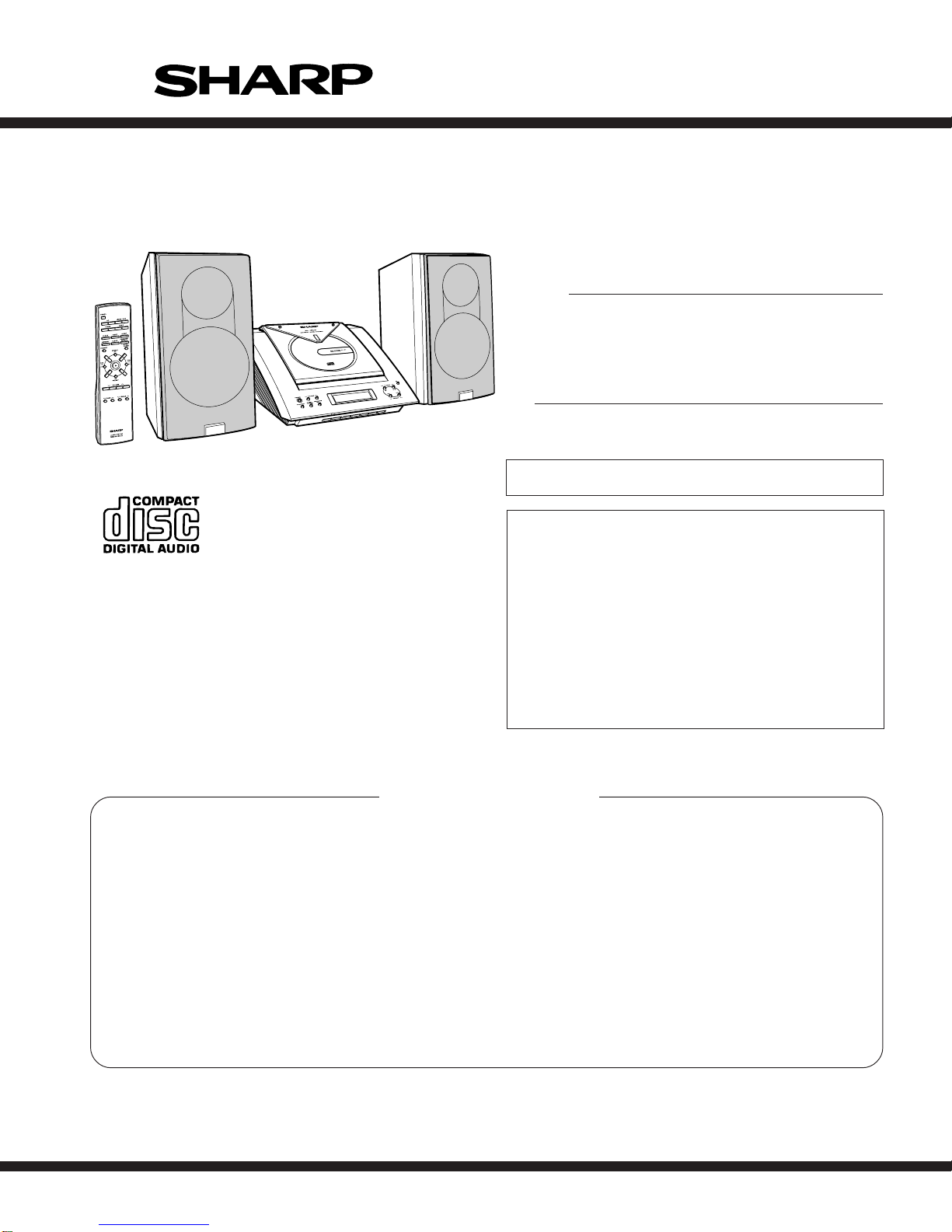
Sharp XL-1200 User manual

– 1 –
XL-1200/1200C
SERVICE MANUAL
SHARP CORPORATION
No. S4127XL1200//
This document has been published to be used
for after sales service only.
The contents are subject to change without notice.
COMPACT AUDIO SYSTEM
• In the interests of user-safety the set should be restored to its original
condition and only parts identical to those specified should be used.
XL-1200 Compact Audio System consisting of XL-1200 (main
unit) and CP-XL1200U (speaker system).
MODEL XL-1200
XL-1200C Compact Audio System consisting of XL-1200C
(main unit) and CP-XL1200U (speaker system).
MODEL XL-1200C
CONTENTS
Page
IMPORTANT SERVICE NOTES (FOR U.S.A. ONLY) ..................................................................................................... 2
SPECIFICATIONS ............................................................................................................................................................ 2
NAMES OF PARTS .......................................................................................................................................................... 3
OPERATION MANUAL..................................................................................................................................................... 5
DISASSEMBLY................................................................................................................................................................. 7
NOTES ON SCHEMATIC DIAGRAM ............................................................................................................................... 9
TYPES OF TRANSISTOR AND LED................................................................................................................................ 9
BLOCK DIAGRAM .......................................................................................................................................................... 10
SCHEMATIC DIAGRAM ................................................................................................................................................. 14
WIRING SIDE OF P.W.BOARD...................................................................................................................................... 22
WAVEFORMS OF CD CIRCUIT..................................................................................................................................... 26
TROUBLESHOOTING .................................................................................................................................................... 27
PARTS GUIDE/EXPLODED VIEW
PACKING OF THE SET (FOR U.S.A. ONLY)
This Service Manual is for the XL-1200/1200C, which is a minor-
modification model of the XL-3000/3000C. This manual, therefore,
describes only the changed points from the service manual. Please
refer to the XL-3000/3000C service manual (No. S4122XL3000U/)
together with this manual.
XL-3000/3000C
Page
REMOVING AND REINSTALLING THE MAIN PARTS .....
9
ADJUSTMENT ............................................................... 10
TEST MODE .................................................................. 11
FUNCTION TABLE OF IC.............................................. 44
LCD SEGMENT ............................................................. 53

XL-1200/1200C
– 2 –
FOR A COMPLETE DESCRIPTION OF THE OPERATION OF THIS UNIT, PLEASE REFER
TO THE OPERATION MANUAL.
IMPORTANT SERVICE NOTES (FOR U.S.A. ONLY)
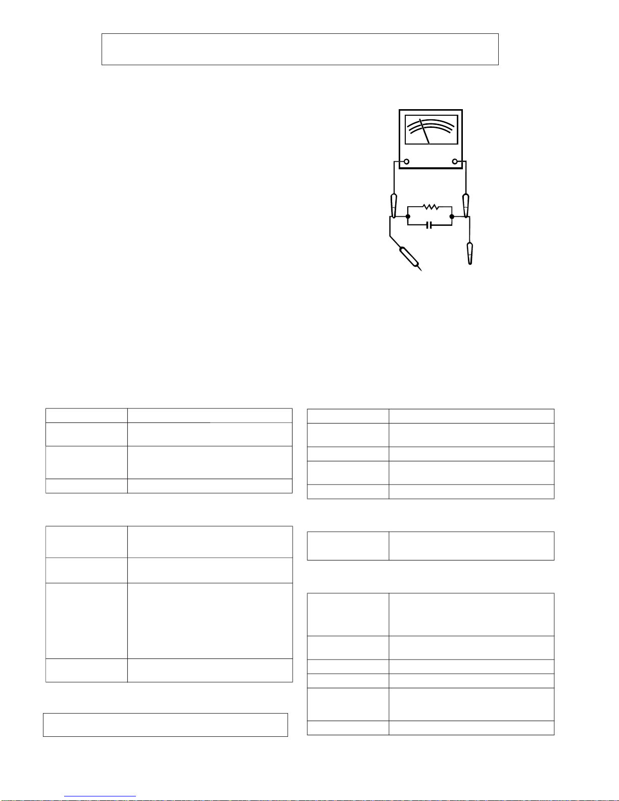
BEFORE RETURNING THE AUDIO PRODUCT
(Fire & Shock Hazard)
Before returning the audio product to the user, perform the following
safety checks.
1. Inspect all lead dress to make certain that leads are not pinched
orthathardwareisnotlodgedbetweenthechassisandothermetal
parts in the audio product.
2. Inspectallprotectivedevicessuchasinsulatingmaterials,cabinet,
terminal board, adjustment and compartment covers or shields,
mechanical insulators etc.
3. To be sure that no shock hazard exists, check for leakage current
in the following manner.
* Plug the AC line cord directly into a 120 volt AC outlet.
* Usingtwoclipleads,connecta1.5kohm,10wattresistorparalleled
by a 0.15µF capacitor in series with all exposed metal cabinet
parts and a known earth ground, such as conduit or electrical
ground connected to earth ground.
* Use a VTVM or VOM with 1000 ohm per volt, or higher, sensitivity
tomeasuretheACvoltagedropacross theresistor(Seediagram).
* Connect the resistor connection to all exposed metal parts having
areturnpathtothechassis(antenna, metal cabinet, screw heads,
knobs and control shafts, escutcheon, etc.) and measure the AC
voltage drop across the resistor.
All check must be repeated with the AC line cord plug connection
reversed.
Any reading of 0.3 volt RMS (this corresponds to 0.2 milliamp. AC.)
or more is excessive and indicates a potential shock hazard which
must be corrected before returning the audio product to the owner.
TO EXPOSED
METAL PARTS
CONNECT TO
KNOWN EARTH
GROUND
TEST PROBE
0.15 µ F
1.5k ohms
10W
VTVM
AC SCALE
■General
■Amplifier
■CD player
■Tuner
■Speaker
Power source AC 120 V, 60 Hz
Power
consumption 33 W
Dimensions Width: 9-1/16" (230 mm)
Height: 5-1/16" (128 mm)
Depth: 11-9/16" (293 mm)
Weight 5.5 lbs. (2.5 kg)
Ou
(For U.S.A)
(For CANADA)
tput power
Output power
16 wat
RMS: 20W (10W + 10W) (10% T.H.D.)
ts minimum RMS per channel into 8
ohms from 100 Hz to 20 kHz, 10% total har-
monic distortion
Output terminals Speakers: 8 ohms
Headphones: 16 - 50 ohms (recommended:
32 ohms)
CD digital output (optical)
Subwoofer (Audio signal): 500 mV/47 ko-
hms
Input terminals Video/Auxiliary (audio signal): 500 mV/47
kohms
Type Compact disc player
Signal readout Non-contact, 3-beam semiconductor laser
pickup
D/A converter 1-bit D/A converter
Frequency
response 20 - 20,000 Hz
Dynamic range 90 dB (1 kHz)
Frequency range FM: 87.5 - 108 MHz
AM: 530 - 1,720 kHz
Type 2-way type speaker system
Tweeter
4" (10 cm) Woofer
Maximum input
power 20 W
Rated input power 10 W
Impedance 8 ohms
Dimensions Width: 5-9/16" (140 mm)
Height: 10-3/8" (263 mm)
Depth: 7-3/8" (187 mm)
Weight 3.8 lbs. (1.7 kg)/each
SPECIFICATIONS
Specifications for this model are subject to change without prior
notice

– 3 –
XL-1200/1200C
NAMES OF PARTS
■
Front panel
1.CD Compartment
2.Volume Up and Down Buttons
3.Power Button
4.Function Selector Button
5.Memory/Set Button
6.Bass/Treble Selector Button
7.CD Play or Pause, Tuning Up Button
8.CD Stop, Tuning Down Button
9.CD Track Down or Fast Reverse,
Tuner Preset Down Button
10.CD Open/Close Button
11.CD Track Up or Fast Forward,
Tuner Preset Up Button
■Display
1.Timer Play Indicator
2.Sleep Indicator
3.CD Random Play Indicator
4.Memory Indicator
5.FM Stereo Mode Indicator
6.CD Play Indicator
7.CD Repeat Play Indicator
8.FM Stereo Receiving Indicator
1
2
3
4
5
6
7
8
9
10
11
12345
7
6 8
■Rear panel
1.Headphone Jack
2.AM Antenna Terminal
3.Antenna Earth Terminal
4.FM 75 Ohms Antenna Jack
5.CD Digital Output Jack
6.Subwoofer Output Jack
7.Video/Auxiliary (Audio Signal) Input Jacks
8.Speaker Terminals
9.AC Power Input Jack
2
1
3
4
5
6
7
8
9

XL-1200/1200C
– 4 –
■Speaker system
1.Tweeter
2.Woofer
3.Bass Reflex Duct
4.Speaker Terminals
Placing the speaker system:
There is no distinction between the right and the left speakers.
4
3
2
1
Speaker grilles are removable:
Make sure nothingcomes into contact with
thespeakerdiaphragmswhen youremove
the speaker grilles.
Left speaker Right speaker
Notes:
●The speakers are magnetically shielded.
Therefore,they donotaffectthe display even if you use them near
the TV. However, some color variation may occur, depending on
the type of TV used.
If color variation occurs...
Turn off the TV (from the power switch).
After 15 - 30 minutes, turn the TV on again.
If the color variation is still present...
Move the speakers further away from the TV.
●If any kind of magnet or an electromagnet is placed too close to
the TV and the system, irregular colors may appear on the TV
screen.
■Remote control
1.Remote Control Transmitter
2.Power Button
3.CD Button
4.Tuner Button
5.Timer Button
6.Clock Button
7.Memory Button
8.Dimmer Button
9.
10.Volume Up and Down Buttons
11.Video/Auxiliary Button
12.Band Selector Button
13.Clear Button
14.Sleep Button
15.Random/Repeat Button
16.CD Open/Close Button
17.Tuner Preset Up Button
18.CD Track Down Button
19.CD Fast Reverse, Tuning Down Button
20.CD Play Button
21.CD Track Up Button
22.CD Fast Forward, Tuning Up Button
23.CD Pause Button
24.CD Stop Button
25.Tuner Preset Down Button
26.Bass Up and Down Buttons
Treble Up and Down Buttons
Buttons with " " mark in the illustration can be operated on the re-
mote control only.
Other buttons can be operated both on the main unit and the re-
mote control.
1
2
3
4
5
6
7
8
9
10
11
12
13
14
15
16 20
21
22
17
18
19
23 24
25 26

– 5 –
XL-1200/1200C
OPERATION MANUAL
Setting the Clock
This may be operated only with the remote control.
In this example, the clock is set for the 12-hour (AM 12:00) display.
To confirm the time display when the power is on:
Press the CLOCK button.
The time display will appear for about 5 seconds.
Note:
The time will flash at the push of the CLOCK button when the AC
power supply is restored after a power failure or unplugging the unit.
Readjust the clock as follows.
To readjust the clock:
Perform "Setting the Clock" from the beginning.
To change the 12-hour or 24-hour display:
1
Press the CLOCK button and within 3 seconds, press
the MEMORY button.
2
Within 1 minute, press the PRESET ( or ) button to
select 12-hour or 24-hour display and then press the
MEMORY button.
"AM 12:00" The 12-hour display will appear.
(AM 12:00 - PM 11:59)
"0:00" The 24-hour display will appear.
(0:00 - 23:59)
Note that this can only be set when the unit is first installed or it
has been reset.
3
Within 1 minute, press the PRESET ( or ) button to
adjust the hour and then press the MEMORY button.
●When the 12-hour display is selected, "AM" will change au-
tomatically to "PM".
4
Within 1 minute, press the PRESET ( or ) button to
adjust the minutes and then press the MEMORY button.
●The hour will notadvance even ifminutes advance from "59"
to "00".
●The clock starts from "0" second. (Seconds are not dis-
played.)
1 Clear all the programmed contents.
2 Perform "Setting the Clock" from the beginning.
Remote Control
■Test of the remote control
Check the remote control after checking all connections have been
correctly.
Face the remote control directly to the remote sensor on the unit.
The remote control can be used within the range shown below:
Press the POWER button. Does the power turn on? Now, you can
enjoy the music.
Remote sensor
8" - 20'
(0.2 m - 6 m )
Troubleshooting Chart
■If trouble occurs
When this product is subjected to strong external interference
(mechanical shock, excessive static electricity, abnormal supply
voltage due to lightning, etc.) or if it is operated incorrectly, it may
malfunction.
If such a problem occurs, do the following:
Caution:
This operation will erase all data stored in memory including clock,
timer settings, tuner preset, and CD program.
1 Set the unit to the stand-by mode and turn the power on
again.
2 If the unit is not restored in step 1, unplug and plug in the
unit, and then turn the power on.
3 If neither step 1 nor 2 restores the unit, do the following:
Press the POWER button to enter the power stand-by mode.
Unplug the AC power cord from the AC INPUT jack on the
unit.
While pressing down the MEMORY/SET button and the
button,plug the AC power cordintotheAC INPUTjack onthe
unit.
AC INPUT

XL-1200/1200C
– 6 –
Accessories
Accesorios
1
1
2
2
Speaker wire × 2
Cable del altavoz
×
2
Remote control × 1
Controlador remoto
×
1
AC power cord × 1
Cable de alimentación de CA
×
1
AM loop antenna × 1
Antena de cuadro de AM
×
1
FM antenna × 1
Antena de FM
×
1
123
Battery installation of remote control
Instalacióndelas pilasdelcontrolador remoto
Use 2 “AAA” size batteries (UM-4, R03, HP-16 or similar).
Use dos pilas del tamaño “AAA” (UM-4, R03, HP-16 o
equivalentes).
Remove the battery
cover.
Extraigala cubierta de
las pilas.
Insert the batteries
as shown.
Inserte las pilas como
se muestra.
Replace the cover.
Vuelva a colocar la
cubierta.
Batteries are not included.
Las pilas no están incluidas.
AM loop antenna
Antena de cuadro
de AM
White line
Línea blanca
Black
Negro
Right speaker
Altavoz derecho
Left speaker
Altavoz izquierdo
AC outlet
(AC 120 V, 60 Hz)
A un tomacorriente de
CA (120 V de CA, 60 Hz)
Right speaker
Altavoz derecho
Left speaker
Altavoz izquierdo
RCA cord
(not supplied)
Cable RCA
(no suministrado)
To the line
output jacks
A las toma de
salida de línea
VCR, DVD, etc.
Videograbadora,DVD,etc.
TV
TV
Connection cable
for digital recording
(not supplied)
Cable de conexión
para grabación digital
(no suministrado)
MD recorder
Grabadora de MD
To the optical line
input jack
A la toma de
entrada de línea óptica
Headphones
Auriculares
System connections
Conexiones del sistema
3
3
FM antenna
Antena de FM
Speaker with a built-in
amplifier
Altavoz con amplificador
incorporado
Press the POWER button to turn the power on.
Pulse el botón POWER para conectar la alimentación.
Listening to a CD
Audición de un disco CD
5" (12 cm)
12 cm
3" (8 cm)
8 cm
Turn on your system
Conexión de la alimentación de su sistema
4
4
Total number of tracks
Número total de pistas
Total playing time
Tiempo total de
reproducción
1
Press the FUNCTION button
until“CDSTOP”or“NO DISC”
appears on the display.
Pulseelbotón FUNCTION hasta
que “CD STOP” o “NO DISC”
aparezca en el visualizador.
2
Press the 77
77
7 button to open
the CD compartment.
Pulse el botón
77
77
7
para abrir el
compartimiento del CD.
3
Place a CD on the spindle,
label side up.
Ponga un CD sobre el eje, con
la cara de la etiqueta arriba.
4
Press the 77
77
7 button to close
the CD compartment.
Pulse el botón
77
77
7
para cerrar
el compartimiento del CD.
5
Press the JJ
JJ
J button to start
playback from track 1.
Pulse el botón
J
para iniciar la
reproducción desde la pista 1.
FM stereo mode indicator
Indicador del modo de FM en estéreo
FM stereo receiving indicator
Indicador de recepción de FM en estéreo
1
Press the FUNCTION button
until “FM” or “AM” appears
on the display.
Pulse el botón FUNCTION
hasta que “FM” o “AM”
aparezca en el visualizador.
2
Press the TUNING (XX
XX
Xor WW
WW
W)
button to tune in to the de-
sired station.
When the TUNING button is
pressed for more than 0.5
seconds, scanning will start
automatically and the tuner
will stop at the first receiv-
able broadcast station.
Pulse el botón TUNING (
X
o
W
) para sintonizar la emisora
deseada.
Cuando se pulse el botón
TUNING durante más de 0,5
segundos, la exploración se
iniciará automáticamente y el
sintonizador se parará en la
primera emisora difusora que
pueda recibirse.
To receive an FM stereo trans-
mission:
Press the FUNCTION button to
display the “ST” indicator.
●“jj
jj
j” will appear when an FM
broadcast is in stereo.
Para recibir una transmisión de
FM en estéreo:
Pulse el botón FUNCTION para
visualizar el indicador “ST”.
●
“
j
” aparecerá cuando una
difusióndeFMseaen estéreo.
Listening to the radio
Audición de la radio

– 7 –
XL-1200/1200C
1
Rear panel/Terminal PWB
1. Screw .................. (A1) x7 7-1
2. Socket ................. (A2) x3
3. Screw .................. (A3) x4 7-1,2
2 Top cabinet 1. Screw .................. (B1) x2 7-2
2. Hook .................... (B2) x5
3. Flat Cable............ (B3) x1
4. Socket ................. (B4) x7
3 Tuner PWB 1. Screw .................. (C1) x2 8-1
2. Socket ................. (C2) x1
4 Power PWB 1. Socket ................. (D1) x1 8-1
2. Hook .................... (D2) x1
5 Main PWB 1. Socket ................. (E1) x1 8-1
2. Screw .................. (E2) x8
6 Display PWB 1. Screw .................. (F1) x4 8-2
2. Hook .................... (F2) x4
7 CD Mechanism 1. Screw .................. (G1) x4 8-2
8 Gear Box 1. Screw .................. (H1) x1 8-2
2. Holder.................. (H2) x1
3. Lever ................... (H3) x1
4. Screw .................. (H4) x2
5. Lever ................... (H5) x1
9 LED PWB 1. Screw .................. (J1) x1 8-2
DISASSEMBLY
STEP REMOVAL PROCEDURE FIGURE
Note:
After removing the connector for the optical pickup from the
connector, wrap the conductive aluminium foil around the
front end of connector remove to protect the optical pickup
from electrostatic damage.
Caution on Disassembly
Follow the below-mentioned notes when disassembling
the unit and reassembling it, to keep it safe and ensure
excellent performance:
1. Take compact disc out of the unit.
2. Be sure to remove the power supply plug from the wall
outlet before starting to disassemble the unit.
3.Take offnylon bandsor wire holderswhere theyneed to
beremovedwhendisassemblingtheunit.Afterservicing
theunit, besure torearrange theleads wherethey were
before disassembling.
4. Take sufficient care on static electricity of integrated
circuits and other circuits when servicing.
(A1) x2
ø3 x10mm
(A1) x3
ø3 x10mm
(A1) x2
ø3 x10mm
Rear Panel
Top Cabinet
(A2) x3
(A3) x3
ø3 x10mm
Rear Panel
Terminal PWB
Figure 7-1
(B1) x2
ø2.5 x8mm
(B4) x2 (A3) x1
ø3 x8mm
Lug
(B4) x4 (B3) x1
Hook
(B2) x3
HOOK
(B2) x2
(B4) x1
CD Mechanism
Main PWB
Power PWB
Hook
Up
Slide
Bottom Cabinet
Top Cabinet
Top Cabinet
Bottom Cabinet
Figure 7-2

XL-1200/1200C
– 8 –
(C1) x1
ø3 x8mm
(E2) x7
ø3 x8mm
(E2) x1
ø3 x14mm
(D2) x1
(C1) x1
ø3 x6mm
(D1) x1
(E1) x1
Power PWB
Holder PWB
Tuner PWB
Main PWB
(C2) x1
Tuner PWB
(C2) x1
Main PWB
Hook
Bottom Cabinet
Figure 8-1
Figure 8-2
(G1) x4
ø2.5 x10mm
(H1) x1
ø3 x8mm
(H2) x1
(H5) x1
(H4) x2
ø2.5 x10mm
(J1) x1
ø2.5 x10mm
(F1) x4
ø2.5 x10mm
Hook
(F2) x4
Display PWB
LED PWB
Switch PWB
Gear Box
CD Mechanism
Bracket
Top Cabinet
Holder PWB
(H3) x1
1 Speaker 1. Net Frame ........... (A1) x1 8-3
2. Front Panel ......... (A2) x1
3. Screw .................. (A3) x4
STEP REMOVAL PROCEDURE FIGURE
( A3 ) x4
ø4 x12mm
Screwdriver
Net Frame
( A1 ) x1
Front Panel
( A2 ) x1
Woofer
Tweeter
Figure 8-3

– 9 –
XL-1200/1200C
NSW801 PICKUP IN ON—OFF
SW709 POWER ON—OFF
SW710 CD LID OPEN/CLOSE ON—OFF
SW711 FF/PRESET UP ON—OFF
SW712 CD PLAY/PAUSE/TUNING UP ON—OFF
SW713 VOLUME UP ON—OFF
SW718 VOLUME DOWN ON—OFF
•The indicated voltage in each section is the one measured
by Digital Multimeter between such a section and the chas-
sis with no signal given.
1. In the tuner section,
( ) : AM mode
: FM stereo mode
2. In the CD section, the CD is stopped.
•Parts marked with “ ” ( ) are important for
maintaining the safety of the set. Be sure to replace these
parts with specified ones for maintaining the safety and
performance of the set.
NOTES ON SCHEMATIC DIAGRAM
•Resistor:
To differentiate the units of resistors, such symbol as K and
M are used: the symbol K means 1000 ohm and the symbol
M means 1000 kohm and the resistor without any symbol is
ohm-type resistor. Besides, the one with “Fusible” is a fuse
type.
•Capacitor:
To indicate the unit of capacitor, a symbol P is used: this
symbol P means micro-micro-farad and the unit of the
capacitor without such a symbol is microfarad. As to
electrolyticcapacitor,theexpression“capacitance/withstand
voltage” is used.
(CH), (TH), (RH), (UJ): Temperature compensation
(ML): Mylar type
(P.P.): Polypropylene type
•Schematic diagram and Wiring Side of P.W.Board for this
model are subject to change for improvement without prior
notice.
REF. NO DESCRIPTION POSITION POSITIONREF. NO DESCRIPTION
SW721 BASS/TREBLE ON—OFF
SW722 MEMORY SET ON—OFF
SW725 CD STOP/TUNING DOWN ON—OFF
SW726 REW/PRESET DOWN ON—OFF
SW727 FUNCTION ON—OFF
SW802 CD LID ON—OFF
ECB
(S)(G)(D)
FRONT
VIEW
FRONT
VIEW
BCE
FRONT
VIEW
2SB562 C
2SC535 C
KRA102 M
KRC102 M
KRC104 M
KRC107 M
KTA1266 GR
KTC3199 GR
KTC3200 GR 2SD2012 Y DB5306X SVC348S
KDV147C
1 2 3
(1) (2) (3)
Figure 9 TYPES OF TRANSISTOR AND LED

XL-1200/1200C
– 10 –
Q801
Q901 Q902
Q908
Q802
Q907
Q861
7654321 8910 11 12 13 14 15
CNP702
CLID_SW
CLID_UP
CLID_PRO
CLID_DW
BUCK
BUS2
BUS0
BUS1
BUS3
CCE
CD_RES
PU_IN
LIGHT
CD_STB
DIMMER
SBAD
FEO
FEN
VRO
RFRP
RFIS
RFGO
RFGC
AGCI
RFO
GND
RFN
TEO
TEN
2VRO
TEB
SEL
LDO
MDI
TN1
TPI
FPI
FNI
VCC
SERVO PRE AMP.
IC801
TA2109F
SERVO/SIGNAL CONTROL
IC802
TC9462F
DOUT
TERMINAL
PWB
VSS
VSS
VSS
AVSS
XVSS
TESIOO
TESIN
TESI01
VSS
VSS
PXI
DVSL
DVSR
PDO
TMAX
VCOREV
RFI
RFCT
LPFN
LPFO
PVREV
TSIN
VREF
X801
16.93MHz XO
XI
VDD
VDD
VDD
VDD
VDD
XVDD
AVDD
2VREF
SEL
RFGC
TEBC
FOO
TRO
TEI
TEZI
RFRP
FEI
SBAD
P2VREF
SWITCHING
R-CH
L-CH
SO401
VIDEO/AUX
INPUT
CD LID
MOTOR DRIVER
1
23
5
67
8
9
IC805
TA7291S
11 10
9 8 7 6 5 4 3
2
CE
CL
DI
SD
FM ST
DO
A_12V
D_GND
TUN L
TUN R
+B6
+B2
+B4
CNP307
TO
TUNER PWB
FROM
DISPLAY PWB
LED PWB
SWITCH PWB
CD LID
OPEN/CLOSE
SW802
D801
CD LID
OPEN/CLOSE
MOTOR
M
M801
FOCUS/TRACKING/
SPIN/SLED DRIVER
1234
5
6
7
8
9
9
10111213
16 17 18 19 21 22 23 24 25 26 27 28
PO1-
PO1+
VO3-
VO3+
VIN3
VG3
VCC
VCC
BIAS
VG4
VIN4
VO4+
VO4-
OPO
VO2-
VO2+
VIN2
VG2
GND
GND
GND
MUTE
REG O
TRB
VG1
VIN1
VO1+
VO1-
IC804
MM1469XH
SPINDLE
MOTOR
SLED
MOTOR
PICKUP IN
SP+
SP–
SP+
SL–
PU-IN
GND
FO
TR
+
–
–
+
M
M
CD MOTOR PWB
NM802
NM801
NSW801
CD_6R2V
5V +B2
+B4
+B7
+
B
+B7
A
C
B
F
E
+B7
+B7
+B7
LD
MON
FOCUS COIL
1/2V
5V
TRACKING COIL
CD PICKUP U
N
23
24
22
21
20
19
18
17
16
45
40
38
34
33
32
31
30
28
50
56
57
51
52
48
49
46
47
43
42
44
15
14
13 12
11
10
9
8
7
6
5
4
3
2
1
DIGITAL
OUT 3
2
1
J801
5355
FMO
DMO
100
90
97
96
93
92
91
78
79
BUS0
BUS1
BUS2
BUS3
BUCK
/CCE
/RST
85
82
RO
LO
14
23
39
62
76
80
94
6152436 63 71 72 73 74 77 95 81 86
A_GNDD_GND
D_GND
M_GND
M_GND
M_GND
M_GND
25
SUB
WOOFER
OUT
Figure 10 BLOCK DIAGRAM (1/4)

– 11 –
XL-1200/1200C
VOLTAGE
REGULATOR
3
1
3
2
1
USWD_5R6V
P_CONT
D_GND
3
2
1
AC INPUT
SOCKET
AC120V,60Hz
AC 120V,60Hz AC POWER SUPPLY CORD
POWER
TRANSFORMER
(SUB)
FROM
DISPLAY PWB
POWER PWB-B
CNP651
SO655
IC681
AN78L05
D688
1N4004
RLY601
CNP707
T681
D681~D684
Q683
Q681
4
3
2
1
4
3
2
1
3
1
POWER
TRANSFORMER
(MAIN)
TF
T651
2.5A 125V
CNP801
F651
1.6A 125V
F653
Q606
Q607
Q904
D651~D654
D657~D660
Q101
Q102
Q601
Q602
Q605
Q603
Q604
Q608
Q609
Q903
CD +B
5V
+B
CD_6R2V
+B1
+B2
+B3
+B4
+B5
+B6
M_12V
A_12V
A_24V
5 12910 11
3 742
IN2
POWER
–GND1,2
VCC
OUT1
FIL
OUT2
GND
IN1
POWER AMP.
IC901
LA4282
L-CH
L-CH
R-CH
R-CH
L-CH R-CH
SPEAKER TERMINAL
+
+
SO601
HEADPHONES
1
2
3
4
5
9
10
J601
VSS
VDD
IC401
LC75342M
15 14 13 12 11 10 9
17 18 19 20 21 22 23 24 25 26 27 28 29
16
8 7 6 5 4 3 2 1
CE
DI
30
CL
LOGIC
TUN L
CD L
TUN R
R-CH OUT
L-CHOUT A_12V
NC
FUNCTION/VOLUME
EQUALIZER
AUX R
AUX L
CD R
MUTE
VOLTAGE
REGURATOR
VOLTAGE
REGURATOR
VOLTAGE
REGURATOR
+B6
4 3 2 1
D
_
GND
TUN L
TUN R
A_GND
4 5 61 2 3 7 8 9
10 11 12
SD
STEREO
DO
CE
DI
CL
CD +B
P_MUTE
P_STB
D_GND
5V
A_24V
+B1
+B3
+B5
CNP703
FROM
DISPLAY PWB
+B7
P
UNIT
D_GND
MAIN PWB
Figure 11 BLOCK DIAGRAM (2/4)

XL-1200/1200C
– 12 –
AM
GND
FM
75ohms
SO301
VSM
AM RF
OUT
OUT
IN
IN
CUT
AM LOW
FM/AM
FM AFC
AM OSC
AM OSC
FM DET
STEREO
SD
GND
AM IF
REG
AM MIX
OUT
IN
IN
FM IF
23 22 21 20 19 1824
8
7654321
PLL(TUNER)
8
765431
PD
FM IN
VDD
AIN
AOUT
VSS
X OUT
22 21 20 19 18 17 1
FM
MUTE
CE
DI
CL
DO
X IN
IC302
LC72131
FM FRONT END
123456 7 9
8
IC301
BF301
BAND PASS
FILTER
TA7358AP
123
TP301
45
6
X
3
32.768kHz
8MHz
38541
1
100
67
3932
47
8
4
LCD701
LCD DISPLAY
TO
POWER PWB
REMOTE
SENSOR
RX701
3
2
1
3
2
1
CNW707
CNS707
RESET
VLC1
VLC2
VLC3
7
6
5
MMOD
VREF
VREF+
VSS
15
24
14
11
SYS_STOP
POWER
3837
13
12
10
9
X701
X702
OSC1
OSC2
XO
XI
CLID_SW
SW711~713
SW721,722
SW725~727
SW709
SW718
SW710 KEY1
KEY2
18
17
16
SYSTEM MICROCOMPU
T
FL DRIVER
IC701
IX0039SJ
A_24V
5
V
DI
CL
DO
CE
28272625
SURR
4
Q708
Q707
Q709
Q706
GND
LMP701
LAMP PWB
ANTENNA
TERMINAL
AM Band
Coverage fL
FM MUTE
LEVEL
AM IF
FM IF
AM
Tracking fL
FM RF
VD301
VD303
VD302
+5V
+5V
VT
+5V
FM +B
+5V
T302
T306
T304
T351
CF303
L302
FM ANT.
FM Band
Coverage fL
FM +B
FM +B
L303
FM OSC.
CF302
FM IF FM IF
CF352
AM IF
SWITCHING
RESET
SWITCHING
Q306
Q302
Q701 Q702
Q703
VR351
X352
4.5MHz
COM0
COM3
SEG0
SEG33
REMOCON
P_CONT
USWD_5R6V
D_GND
P–CONT
VDD
Figure 12 BLOCK DIAGRAM (3/4)

– 13 –
XL-1200/1200C
VSM
AM
RF
OUT
OUT
OUT
IN
CUT
AM LOW
FM/AM
MPX VCO
MPX IN
MO/ST
L-CH
R-CH
(AM/FM)
PHASE
PHASE
IF OUT
VCC
FM DET
STEREO
SD
GND
AM IF
IN
2
1201918 17 16151413
121110987654
11109876543
PD
IF IN
AM IN
FM IN
VDD
AIN
AOUT
20 19 18 17 16 15 14 13 12
FM
FM
MUTE
CE
DI
CL
DO
MO/ST
IF REQ
456kHz
X351
Q351
Q360
ZD351 10
11
1
2
3
4
5
8
9
6
7
SD
FM ST
DO
CL
CE
DI
A_12V
D_GND
TUN_L
TUN_R
A_GND
TO
MAIN PWB
CNS307
TUNER PWB
385
100
67
57
56
20
59
66
65
64
63
62
61
60
58
53
54
51
40
48
23
39 46 49 50
LCD701
LCD DISPLAY
1
2
3
4
5
6
7
8
9
10
11
12
13
14
15
LIGHT
BUS0
BUS1
BUS2
BUS3
BUCK
CCE
CD_STB
CLID_DW
CLID_UP
CLID_PRO
CLID_SW
CD_RES
PU-IN
DIMMER
LIGHT
BUS0
BUS1
BUS2
BUS3
BUCK
CCE
CD_STB
CLID_DW
CLID_UP
CLID_PRO
CD_RES
PU-IN
DIMMER
B-LIGHT
1
2
3
4
5
6
7
8
9
10
11
12
13
14
15
TO
MAIN PWB
TO
MAIN PWB
CNS702
CNW702
SYS_STOP
POWER
3837
S
TEM MICROCOMPUTER/
FL DRIVER
IC701
IX0039SJ
D_GND
A_24V
5V
A_24V
5V
VSM
DATA
CLE
P_STB
P_MUTE
CD+B
DI
CE
CL
DO
STEREO
SD
12
11
10
9
8
7
6
5
4
3
2
1
12
11
10
9
8
7
6
5
4
3
2
1
CNW703
CNS703
CD+B
STEREO
SD
DI
CL
DO
CE
28272625
SURR
P–STB
P–MUTE
454443
DISPLAY PWB
Q709
FM IF DET/
FM MPX/AM IF
IC303
LA1832S
+5V
+5V
+B
FM +B
+5V
CF352
CF351
AM IF
SWITCHING
H
ING
VOLTAGE
REGURATOR
COM3
SEG0
SEG33
REMOCON
Figure 13 BLOCK DIAGRAM (4/4)

XL-1200/1200C
– 14 –
A
B
C
D
E
F
G
H
123456
• NOTES ON SCHEMATIC DIAGRAM can be found on page 9.
1.6A 125V
2.5A 125V
13V
20V 12.3V
12.2V
11.7V
20V
20V
20V 7.1V
7.9V
7.7V
9.3V
9.4V
9.4V
11.7V
+B
+B
+B
+B
4.9V
5.6V
11.2V
+B
24.4V
38.9V
24.9V
+B +B
+B
+B
+B
+B
+B
0V
4.8V 0V
+B
0.6V
9.2V
5.7V
0.7V
0.72V
0V
9.2V
0.11V
0V
VOLTAGE
REGULATOR
AC POWER SUPPLY CORD
4
3
2
1
4
3
2
1
+BGND
+B2
3
2
1
+B1
11 10
9 8 7 6 5 4 3 2 1
CE
CL
DI
SD
FM ST
DO
A_12V
D_GND
TUN L
TUN R
A_GND
1 2 3 4 5 6 7 8
SD
STEREO
DO
CE
DI
CL
CD +B
P_MUTE
2
1
32
1
3
3
1
3
1
POWER
TRANSFORMER(MAIN)
3
2
1
USWD_5R6V
P_CONT
NOT
CONNECT
D_GND
3
2
1
POWER
TRANSFORMER
(SUB)
CNS307
P19 12-E TO
TUNER PWB-A2 CNS703
P21 12-FFR
O
DI
S
CNS707
P20 1-E FROM
DISPLAY PWB-A3
POWER PWB-B
TF
CHASSIS
GND
3
2
1
3
2
1
2
1 2
1
DIGITAL OUT
VIDEO/
AUX IN
SUB
WOOFER
OUT
L-CH
R-CH
2
1
3
2
1
3
2
1
CNS805
P16 1-G
FROM
MAIN PWB-A1(2/2)
TERMINAL PWB-A4
TO CHASSIS GND
LUG(205)
TO CHASSIS GND
LUG(205)
TO CHASSIS GND
LUG(205)
AC INPUT SOCKET
AC 120V,60Hz AC 120V,60Hz
CNW607
Q605
2SD2012 Y
R619
47
R620
47
F653
C125
2200/50
D658
R401
1K
R402
1K
C902
220/50
R910
2.7K
D902
1N4004
C903
10/50
D901
1N4004
C901
220/50
R911
100
C904
10/50
ZD901
DZ24BSD
Q904
KTC3200 GR
C906
100/10
R913
10
ZD902
DZ5.6BSB
R912
470
Q903
KTC3199 GR
C905
100/10
C630
4700/25
C620
470/25
CNP307
CNP801
D653
1N5402M
D652
1N5402M
D654
1N5402M
D651
1N5402M
C654
0.1 C651
0.1
F651
C660
0.1
C659
0.1 C658
0.1
C657
0.1
D660
D659
D657
1N4004
1N4004
1N4004
1N4004
Q604
2SD2012 Y
R623
22K
C624
0.022
C625
10/16
R629
820
ZD601
DZ130BSA
C622
0.022
Q603
KTC3200 GR
R628
100
C621
100/25
D602
1N4148
R617
33K
R624
22K
C627
0.022
C629
470/25
R611
100
R612
820
R613
33K
C626
100/25
Q608
KRA102 M
R621
22K
Q606
KTC3200 GR
Q607
2SD2012 Y
R614
47
D604
1N4148
ZD602
DZ8.2BSC
Q609
KRC107 M
C628
10/16
CNP651
T651
D681
1N4004
D683
1N4004
C661
0.001
D682
1N4004
D684
1N4004
C683
2200/16
SO655
IC681
AN78L05
R687
2.7K
ZD683
MTZJ16C
R689
1K
ZD684
MTZJ16C
Q681
KTC3199 GR
R688
1K
C689
0.47/50
D688
1N4004
C665
0.047
C688
0.047
R685
10K
Q683
KTC3199 GR
R686
47K
RLY601
D685
1N4004
D689
1N4004
CNP707
T681
CNP805
CNW704
CNP607
CNP704 CNS704
CNS607
C853
0.0047
R406
27K
R405
27K
R410
1K
R408
2.2K R407
2.2K
R411
1K
SO401
C413
0.0047
C410
0.0047
C852
0.0022
C412
330P
C411
330P
L802
0.82µH
C851
100/10
C414
0.45/50
J801
CFW852
CFW451
CFW452
R652
4.7M
(1/2W)
Figure 14 SCHEMATIC DIAGRAM (1/8)

– 15 –
XL-1200/1200C
78 9 10 11 12
4.8V
4.8V
0V
0V
4.8V
4.8V
4.8V
4.8V
0V
0V
5V
4.8V
4.8V
4.8V
4.8V
4.8V
4.8V
4.8V
4.8V
0V
0V
0.14V
0.14V
4.8V
9.6V
4.8V
4.8V
4.8V
4.8V
4.8V
+B
+B
+B
+B
+B
4
.9V
V
+B
0V
0.6V
0.6V
0.6V 17.7V
23.2V 23.2V
0V
0V
0V
1.14V
0.74V
17.7V
0V
0V
1.14V
0V
17.6V
0V
36V
17.6V
0.74V
0V0V
+B +B
B
+B
CD SIGNAL
121110
98765421 3
POWER
–GND1
POWER
–GND2
OUT1
MUTE
OUT2
NF2
IN2
GND
VCC
FIL
NF1
IN1
16 17 18 19 20 21 22 23 24 25 26 27 28
15 14 13 12 11 10
9 8 7 6 5 4 3 1
29 30
2
CL
VDD
VREF
ROUT
RBS2
RBS1
RTRE
RIN
RSL0
R4
R3
R2
R1 L1
L2
L3
L4
LSL0
LIN
LTRE
LBS1
LBS2
LOUT
TEST
VSS
CE
DI
1 2 3 4 5 6 7 8 9
10 11 12
SD
STEREO
DO
CE
DI
CL
CD +B
P_MUTE
P_STB
D_GND
5V
A_24V
AUX L
AUX R
TUN R
CD R
AUX L
CD L
TUN L
L
R
+B
M_GND
M_12V
A_GND
CD_L
CD_R
CD_6R2V
CD_GND
7
6
4
3
2
1
8
5
CE
DI
CL
HEADPHONES
CHASSIS
GND
L-CH
R-CH
1
2
3
4
5
9
10
CNS703
P21 12-FFROM
DISPLAY PWB-A3
MAIN PWB-A1(1/2)
TO
MAIN PWB-A1(2/2)
P16 1-E
P17 11-C
SPEAKER TERMINAL
FUNCTION/
VOLUME
EQUALIZER
POWER AMP.
FM SIGNAL
+
+
2
1
1
3
2
3
C432
220P
C431
220P
C433
220P
CNP703
R662
330
R661
330
SO601
R425 1K
R424 1K
C906
100/10
B
G
R
C905
100/10
IC901
LA4282
C416
10/16
C401
10/16
C112
10/50
C603
100/16
R607
6.8K
R604
10K
R110
22K
R109
820
R603
10K
R609
1K
R608
1K
Q602
KTC3199 GR
Q601
KTC3199 GR
R634
10K
J601
L603
10µH
R417
1K
R637
4.7
L601
3µH
C403
10/16
C407
10/16
C408
10/16
C404
10/16
C402
10/16
R422
1K
R415
1K
R416
1K
R418
1K
R421
1K
IC401
LC75342M
C415
10/16
C417
2.2/50
C419
0.0027 C421
0.1(ML)
C423
0.1(ML)
C425
10/16
C430
100/16
D403
1N4004
R439
3.9K
R437
6.8K
C429
33/16
R438
6.8K
C418
2.2/50 C420
0.0027
C426
10/16
C422
0.1(ML)
C424
0.1(ML)
R440
3.9K
R423 1K
R435
10K
R436
10K
D402
1N4004
D401
1N4004
R101
1K
R102
1K R104
56K
R106
4.7 R107
270
R105
270
L602
3µH
R638
4.7
C613
0.1
C615
0.1
C614
0.1
C616
0.1
C104
0.082
C107
0.082
C113
0.022
C101
0.022
C117
470P
C118
470P
C103
100/25
C108
100/25
C109
470/25
C114
470/25
C102
47/25
C120
680P
C119
68P
C110
0.1
C111
0.1
R108
4.7
C115
0.1
C116
0.1
C628
10/16
Q102
KRC102 M
Q101
KRC102 M
R635
27K
R636
27K
Figure 15 SCHEMATIC DIAGRAM (2/8)

XL-1200/1200C
– 16 –
A
B
C
D
E
F
G
H
123456
0V
0V
5V
2.2V
2.6V
2.1V
1.8V
2.1V
2.1V
2.1V
2.1V
0V
0V
0V
0V
0V
0V
0V
0V
0V
0V
0V
0V
5V
5V
5V
5V
5V
5V
1.4V
1.7V
2.5V
2.5V
1.2V
2.4V
0.6V
4.3V
2.1V
2.1V
0V
5V
2.1V
2.1V
2.1V
2.1V
2.1V
2.1V
2.1V
2.1V
1.4V
2.2V
2.2V
2.2V
2.2V
2.1V 2.1V
2.1V
0V
0V
0V
0V
0V
0V
0V
0V
0V
0V
0V
0V
0V
0V
5V
5V
5V
5V
5V
2.5V
2.1V
2.2V
4.3V
5V
5V
4.9V
0V
0V
0V
5V
5V
5V
5V
2.3V
2.4V
4.3V
4.3V
4.3V
4.3V
4V
3.3V
0V
2.4V
+B
0V
11.6V
11.6V
6.1V
4.6V
4.8V
0.57V
0V
0V
+B
+B
+B
+B
+
+B
+B +B
0V
0V 4.5V
4.9V
0V
0V
4.1V
SERVO/SIGNAL CONTROL
CD LID
MOTOR DRIVER
1
3
23
1
2
3
TO MAIN PWB-A1(1/2)
BUCK
BUS2
CCE
BUS1
BUS0
CD_RES
BUS3
CLID_SW
CLID_UP
CLID_PRO
CLID_DW
BUCK
BUS2
BUS0
BUS1
BUS3
CCE
CD_RES
PU_IN
LIGHT
7
6
5
4
3
2
1
8
9
10
11
12
13
14
15
123456789
CD_STB
28 29 302625 2723222120199 1011121314 2415 16 17 1812345678
53 52 515556 54585960616272 71 70 69 68 67 5766 65 64 6380 79 78 77 76 75 74 73
TESTO
/HSO
UHSO
EMPH
LRCK
VSS
BCK
AOUT
DOUT
MBOV
IFP
SBOK
CLCK
VDD
VSS
DATA
SFSY
SBSY
SPCK
SPDA
COFS
MONIT
VDD
TESIO0
P2VREF
HSSW
ZDET
PDO
TMAXS
TMAX
VCOREV
VCOF
AVSS
SLCO
RFI
AVDD
RFCT
RFZI
RFRP
FEI
SBAD
TSIN
TEI
TEZI
FOO
100
90
99
100
99
97
96
95
94
93
92
91
89
88
98
87
86
85
84
83
82
81
82
81
DVDD
DVSL
DVR
TEST1
TEST2
TEST3
BUS0
BUS1
BUS2
BUS3
VDD
VSS
BUCK
/CCE
TEST4
RFGC
TEBC
FMO
FVO
DMO
2VREF
SEL
FLGA
FLGB
FLGC
VDD
VSS
IO0
IO1
IO2
IO3
/DMOUT
/CKSE
/DACT
TESIN
TESIO1
VSS
PXI
PXO
VDD
XVSS
XVDD
XO
XI
FLGD
TRO
VREF
50
49
50
49
48
47
46
45
43
42
41
40
39
38
37
36
35
34
44
33
32
31 LPFN
LPFO
/RST
/TSMOD
DVSR
RO
3
2
1
3
8
2
1
DIMMER
CNP805 P15 12-G
P14 3-A,BTO
TERMINAL PWB-A4
CNS702
P21 12-CFROM
DISPLAY PWB-A3
PVREV
LO
16.93MHz
R817
1.2K
C864
220P
C866
220P
C869
220P
C862
0.001
C867
220P
C868
220P
C865
220P
C822
220/10
L806
10µH
R832
1K R831
1K
R830
1K
R834
1K
R835
1K
R836
1K
R837
1K
C837A
100/10
CNP702
R833
1K
C823
0.01
R879
3.3K
IC805
TA7291S
Q908
KRC102 M
K
R
Q802
KRC102 M
R
2
R9
4
7
CNW805
CNS805
C813
100/10
C805
0.0027
C807
0.033
C817
0.1
R811
2.2K
C818
0.1
R814
3.3K
C811
47/10
C820
0.01
C825
0.056
C834
470P
L801
10µH
C828
100/10
C863
470P
C835
0.056
R807
10K
R813
10
C850
C803
47/10
R819
220
C836
100/10
C840
100/10
R852
100K
C838
47/10
C829
100/10
C821
0.1
R812
3.3K
C804
0.01
R815
10K
C830
0.056
C802
0.015
C819
0.1
C809
0.0047
R855
100K
C824
0.056
R873
3.3K
C833
470P
R874
2.2K
R808
3.3K
R809
10K
R851
330
X801
R853
100K
R820
1K
C831
10/16 C832
10/16
C872
0.1
L803
10µH
R816
10K
C801
100P
R806
15K
C837
470P
C810
0.001
C826
15P(CH)
R801
10K
C827
15P(CH)
C871
47/16
R818
1.2K
R854
100K
IC802
TC9462F
C806
0.0047
R810
3.3K
R804
100K
C812
0.01
R802
47K
C887
0.0027
C861
0.0022
L808
2.2µH
12
13
16
17 14
4
11
1
6
75
15
• The numbers 1 to 17 are waveform numbers shown in page 26.
• NOTES ON SCHEMATIC DIAGRAM can be found on page 9.
Figure 16 SCHEMATIC DIAGRAM (3/8)

– 17 –
XL-1200/1200C
78 9 10 11 12
5V 6.3V
3.4V 4.1V
2V
2.1V
2.1V
2.1V
2.1V
2.1V
2.1V
2.1V
2.1V
2.1V 2.1V
2.1V
2.1V
2.1V
2.1V
2.1V
2.2V
2.2V
1.7V
0V
0V
5V
2.5V
4.3V
3.4V
+B+B
+B+B
+B
1.9V
0.8V
1V
3.2V
3.2V
3.2V
3.2V
2.1V
2.1V
2.1V
2.1V
2.1V
7.0V
7.0V
4.4V
2.3V
2.1V
6.4V
5V
4.8V
0V
0V
0V
6.5V
2.1V
2.1V
3.1V
3.2V
6.4V
+B
+B
+B
+B +B
+B
+B
V
0V
0V
0V
0V
4.1V
10.7V
10.6V
11.4V
11.4V
11.4V10.7V
FOCUS/TRACKING/
SPIN/SLED DRIVER
SERVO PRE AMP.
CD SIGNAL
1
23
1
2
3
SPINDLE
MOTOR
SLED
MOTOR
PICKUP IN
TR–
+5V
E
A
B
F
C
GND
PD
VR
LD
FO–
TR+
FO+
C
1/2V
C
+5V
E
A
B
F
C
TR-
GND
PD
VR
LD
FO-
FO+
TR+
-
-
-
-
-
+
+
+
+
+
VCC LD
MON
GND
E
A
B
F
C
1/2VCC
ACTUATOR
TR-
FO-
PO+
TR+
CD PICKUP UNIT(308)
M_GND
CD_R
A_GND
D_GND
CD_L
CD_6R2V
M_12V
1234
5
6
7
8
91011121314
15 16 17 18 19 20 21 22 23 24 25 26 27 28
PO1-
PO1+
VO3-
VO3+
VIN3
VG3
VCC
VCC
BIAS
VG4
VIN4
VO4+
VO4-
OPO
VO2-
VO2+
VIN2
VG2
GND
GND
GND
MUTE
REG O
TRB
VG1
VIN1
VO1+
VO1-
GND
PU-IN
SL–
SL+
SP–
SP+ SP+
SP–
SP+
SL–
PU-IN
GND
6
5
4
3
2
1
6
5
4
3
2
1
6
5
4
3
2
1
+
–
–
+
M
M
2
1
2
1
7
6
5
4
3
2
1
3
2
1
3
2
1
3
2
1
1
2
1
22
1
VREF
13
14
15
16
12
11
10
1
2
3
4
5
6
7
8
9
13
14
15
16
12
11
10
1
2
3
4
5
6
7
8
9
23
24
22
21
20
19
18
17
16
15
14
13 12
11
10
9
8
7
6
5
4
3
2
1
MAIN PWB-A1(2/2)
CD MOTOR PWB-C
LED PWB-A6
SWITCH PWB-A5
TO
MAIN PWB-A1(1/2)
P15 12-G,H
CD LID
OPEN/CLOSE
MOTOR
CD LID
OPEN/CLOSE
M
R861
2.2K
R863
2.2K
M801
CNW806
CNP701
CNS701 CNW701
CNP806 CNS806
CNW804
CNP804 CNS804
D801
DB5306X
Q908
R
C102 M
Q901
KRC102 M
Q902
KTA1266 GR
R902
47K
R901
2.2K
R914
470
Q907
KTA1266 GR
R904
2.2K
R905
47K
C841
100/10
R822
33
R80C
82K
R80F
82K
R80B
68K
R821
150
C842
47/10
CNP802 CNW3
R80A
82K
R80G
68K
C857
47/16
C858
0.01
R862
2.2K
Q861
2SB562 C
C813
100/10
1
0
R80E
82K
Q801
KTA1266 GR
L801
10µH
R824
27K
C863
470P
C847
0.1
C859
470/10
C850
220/10
SW802
R877
68K
CNS803
CNW803
CNP803
C846
0.1
R828
1.2K
C844
0.0068
C860
0.1
C843
0.1
R823
1K
C845
100/10
R876
150K
L803
10µH
R827
39K
R825
82K
IC801
TA2109F
R829
68K C839
2P
C849
0.056 C855
100/10
C848
39P
R843
1K
C812
0.01
R826
2.7K
IC804
MM1469XH
NM802
NM801
NSW801
C870
0.001
2
10
9
8
3
Figure 17 SCHEMATIC DIAGRAM (4/8)

XL-1200/1200C
– 18 –
A
B
C
D
E
F
G
H
123456
5V
2.5V
5V
21V
2.1V
5.2V
0V
0V
0V
0V
5.2V
2.1V
5.2V
5.2V
0V
1.5V
1.5V
0.8V
3.8V
4.4V
2.
6
+B
+B
+B
FM IF DET/
FM MPX/AM IF
FM FRONT END
PL
L
FM IF FM IF
FM IF
FM RF
FM
Band
Coverage
FM ANT. FM OSC.
1
2
3
1
2
3
OUT
IN
AM OSC
AM OSC
REG
AM MIX
OUT
IN
FM IF
1
123 4 56 7 8 9
2
3
2324
21
AM
GND
FM
75ohms
TP301
CHASSIS
GND
FM Mute
Level
AM Band
Coverage
AM
Tracking
ANTENNA
TERMINAL
BAND PASS
FILTER
4.5MHz
SO301
C360
C362
3.3/50
C349
0.001
D306
1N4148
D305
1N4148
BF301
C351
0.022 R351
5.6K
VR351
10K(B)
L353
1mH
C319
18P(CH)
C316
10/16
C315
100P
C318
5P C300
0.001
C303
0.001 C312
33P
T304
C304
0.01
C314
22P
(CH)
R310
4.7K
R305
680
R308
10K
R304
47K
R301
22
CF303
R309
470
R313
680
R314
33
R302
100K
Q306
2SC535 C
Q302
2SC535 C
R323
68K
C334
27P(UJ)
C335
560P
C337
0.022
T306
C329
0.022
C331
0.047
C332
0.022
I
C
L
C
IC303
LA1832S
IC301
TA7358AP
C302
0.001
CF302
D301
1N4148
D302
1N4148
C330
12P(CH)
T302
C352
10/16
R358
8.2K
C343
33P
R382
330
C317
0.022
C313
6P(UJ)
C311
10P(CH)
C306
7P(UJ)
C305
0.0047
C307
0.0047
C308
0.022
C309
0.001
C310
0.022
R386
330
R316
330
R312
2.2K
R307
47
R306
10
R303
33K
R315
33
X352
C381
12P(CH)
C382
15P(CH)
C384
0.001
R336
5.6K
C301
0.012
VD301
SVC348S
VD302
KDV147C
L303
L302
VD303
KDV147C
• NOTES ON SCHEMATIC DIAGRAM can be found on page 9.
Figure 18 SCHEMATIC DIAGRAM (5/8)

– 19 –
XL-1200/1200C
78 9 10 11 12
0.6V
2.3V
2.3V (0V)
1.3V
1.3V
4V
(2.2V)
0V (0.9V)
5V
2.1V (2.7V)
2.1V (2.7V)
2.1V
(1.2V)
3.8V
(1.9V)
3.8V
(4.3V)
2.9V
0V
0V
5V
5V
5V
5V
2.1V
2.1V
0V
(0V)
3.7V
4.7V
(0V)
3.9V
(0V)
(0V)
3.5V
0V
0V
0V
3.7V
(11.4V)
1.7V
5.1V
4.8V
0.1V
0.1V
2.6V
0V
2.6V
0.9V
0.9V
5.2V
2.6V
(2.6V)
0V
0V
(0V)
10.8V
10.9V
11.7V
+B
+B
+B
+B
+B
+B
PLL(TUNER)
AM IF
AM IF
1
2
3
10
11
1
2
3
4
5
8
9
6
7
SD
FM ST
DO
CL
CE
DI
A_12V
D_GND
TUN_L
TUN_R
A_GND
VSM
AM RF
OUT
OUT
OUT
OUT
IN
IN
CUT
AM LOW
FM/AM
MPX VCO
MPX IN
MO/ST
L-CH
R-CH
FM AFC
AM OSC
(AM/FM)
PHASE
PHASE
IF OUT
VCC
FM DET
STEREO
SD
GND
AM IF
REG
AM MIX
OUT
IN
IN
1110987654321
PD
IF IN
AM IN
FM IN
VDD
AIN
AOUT
VSS
X OUT
22 21 20 19 18 17 16 15 14 13 12
AM SIGNAL
FM SIGNAL
CNP307
P14 5-A
TO
MAIN PWB-A1(1/2)
TUNER PWB-A2
FM
FM
MUTE
CE
DI
CL
DO
MO/ST
IF REQ
X IN
23 22 21 20 19 18 17 16 15 14
2
4 13
12111098765432
M
Hz
456kHz
23
1
C367
1/50
R350
2.7K
C360
0.022
C362
3.3/50
CNS307
R366
2.2K
C372
1/50
C371
1/50
C398
100/10
C380
10/16
D308
1N4148
C391
47/16
X351
R361
5.6K
C368
1/50 R356
1K R357
470K
R362
5.6K
C369
56P C374
0.027
C373
0.027
C366
0.001
IC302
LC72131
R353
270
T351
CF352
C350
0.022
C352
10/16
R352
1K
C353
0.022
C354
0.022
CF351
C363
0.022
C364
10/16
C365
0.022
C361
0.022
R
382
3
0
C394
47/16
C397
0.022
386
3
0
R381
10K
C393
1/50 R380
1.5K
R379
2.2K
C392
0.001
C387
0.022
C385
0.01
R377
5.6K
R355
3.3K
C357
2.2/50
C358
1/50
C399
0.022
C356
0.001
R393
1K
R395
47K
L351
100µH
C370
1/50
C355
22P
C383
0.022
R387
5.6K
L352
100µH
C395
0.022
C396
100/10
ZD351
DZ5.1BSB
R391
390
R392
390
Q351
KRC104 M
R363
3.3K
R364
3.3K
C386
330P
R365
10K
5
2
1
(CH)
8
2
(CH)
R374
1K
R373
1K
R372
1K
R371
1K
R359
1.8K
R360
4.7K
8
4
01
Q360
KTA1266 GR
R385
5.6K
R384
6.8K
R383
5.6K
R376
10K
Figure 19 SCHEMATIC DIAGRAM (6/8)

XL-1200/1200C
– 20 –
A
B
C
D
E
F
G
H
123456
+B
+B
+B
+B
+B +B
+B
1.1V
0V
0V
0.1V
0.1V
4.1V
4.5V
0.4V
0.4V
+B
+B
+B
+B
+B
2.47V
2.47V
2.47V
2.47V
0V
0V
0V
0V
0V
0V
0V
4.9V
0V
0V
0V
0V
0V 2.5V
2.5V
2.5V
2.5V
2.5V
2.5V
2.5V
2.5V
2.5V
2.5V
5V
4.9V
4.9V
4.9V
4.9V
4.9V
1.7V
3.25V
5V
5V
5V
5V
5V
5V
2.49V
2.47V
2.24V
2.47V
0V
0V
4.8V
5V
0.4V
0.4V
24.5V 24.5V
23.7V
4.2V
5V 5V
24V
5V
GND
123
123
FUNCTION
MEMORY/SET
REW
PRESET DOWN
CD STOP
TUNING DOWN
BASS/TREBLE FF
PRESET UP
CD PLAY/ PAUSE
TUNING UP
VOLUME DOWN
VOLUME UP
POWER
CD LID
OPEN/CLOSE
CLID_PRO
VDD
VLC1
VLC2
VLC3
COM0
COM1
COM2
COM3
OSC1
MMOD
VREF+
OSC2
CLID_SW
DI
KEY1
MODEL
KEY2
VREF
XO
XI
VSS
VSM
25
24
23
22
21
20
19
18
17
16
15
14
13
12
11
10
9
8
7
6
5
4
3
2
1
SEG0
SEG1
SEG2
SEG3
SEG4
SEG5
SEG6
SEG7
SEG8
SEG9
100
99 98 97 96 95 94 93 92 91
RESET
CL
DO
CE
3
5
343332313029282726
P_CONT
3
2
1
3
2
1
5V
5V
1
4
13121110987654321
321
LAMP PWB-A7
3
2
1
3
2
1
3
2
1
REMOTE
SENSOR
USWD_5R6V
D_GND
CNP707
P14 1-F TO
MAIN PWB-A1(1/2)
SYSTE
M
32.768kHz
8MHz
C705
0.01
R718
1.5K
R7A3
100
LMP701
L702
2.2µH
X701
R799
1K
R720B
1.2K
R719
1.2K
R710
2.7K
R796
1K
CFW701A
R797
2.2K
R798
4.7K Q709
KRC102 M
Q708
KTA1266 GR
R729
47K
R732 1K
R731 1K
R733 1K
R734 1K
R721
10K
SW721
SW725
R708
2.2K
R707
2.7K
R778 47K
R779
47K R780 47K
R7A6
1K
R7A9
3.3K
CNW707
CNS707
D721
1N4148
R7A7
1K
R740 1K
R739 1K
R7A0
1K
Q702
KTC3199 GR
C715
100/10
R7A8
82 C714
560P
C713
10/16
R7B0
10K
C712
0.01
ZD701
DZ3.3BSB
R7A1
1K
R7A4
120
R7A5
10K
R738 1K
C702
22P
(CH)
R706
3.9K
Q703
KTC3199 GR
R744 1K
R727
47K
SW709
SW727
R702
10K
R728 1K
C701
22P(CH)
RX701
Q701
KRC102 M
R711
1.2K
C703
0.1
SW711
R722
10K
SW726
SW722
X702
R735
1K
Q706
KRC102 M
R793
10K
R792
47K
Q707
KTA1266 GR
R723 47K
R7A2
100K
C711
3.3/50
D722
1N4148 D723
1N4148
SW713
SW712
R720A
1.2K
SW718
D720
1N4148
C710
0.01
R781
47K
R783
33K
C704
0.022
SW710
R795
47K
R741 1K
CFW701B
• NOTES ON SCHEMATIC DIAGRAM can be found on page 9.
Figure 20 SCHEMATIC DIAGRAM (7/8)
Other manuals for XL-1200
2
This manual suits for next models
1
Table of contents
Other Sharp Stereo System manuals

Sharp
Sharp CD-M4000W User manual

Sharp
Sharp XL-UR250H(BK) User manual

Sharp
Sharp CD-C430H User manual

Sharp
Sharp XL-ES5 User manual

Sharp
Sharp XL-UH240W User manual

Sharp
Sharp QT-CD121H User manual

Sharp
Sharp CD-SW250DVD User manual

Sharp
Sharp CD-BK250W User manual

Sharp
Sharp XL-UR27H User manual

Sharp
Sharp XL-UH06H User manual

Sharp
Sharp WF-971T User manual

Sharp
Sharp MD-M3H User manual

Sharp
Sharp VZ-3000H/E User manual

Sharp
Sharp DK-KP82P User manual

Sharp
Sharp CD-ES111H User manual

Sharp
Sharp XL-1200C User manual

Sharp
Sharp CD-BK100W User manual

Sharp
Sharp CD-BA2100 User manual

Sharp
Sharp XL-MP15H User manual

Sharp
Sharp XL-MP100H User manual