Sharp GX-CD1200W BK User manual

GX-CD1200W
– 1 –
CONTENTS Page
SPECIFICATIONS ...............................................................................................................................................................1
VOLTAGE SELECTION.......................................................................................................................................................2
AC POWER SUPPLY CORD AND AC PLUG ADAPTOR ...................................................................................................2
FITTING OF DIAL POINTER ...............................................................................................................................................2
NAMES OF PARTS .............................................................................................................................................................3
DISASSEMBLY....................................................................................................................................................................4
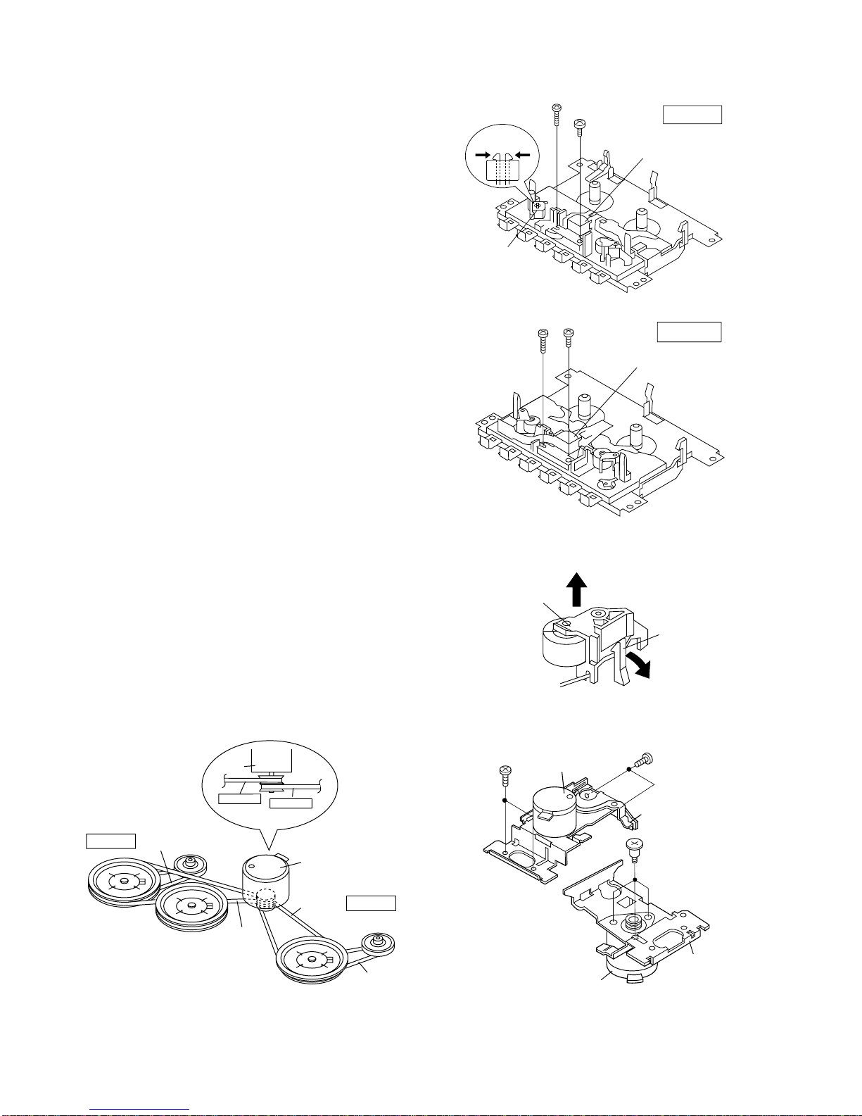
REMOVING AND REINSTALLING THE MAIN PARTS.......................................................................................................5
ADJUSTMENT .....................................................................................................................................................................6
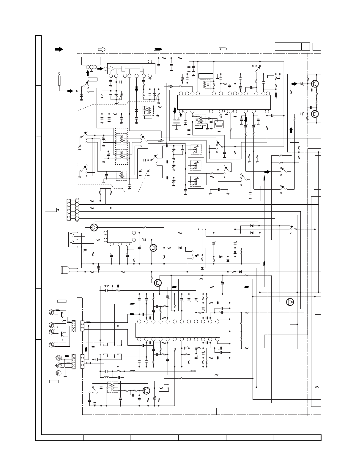
SCHEMATIC DIAGRAM / WIRING SIDE OF P.W.BOARD...............................................................................................10
NOTES ON SCHEMATIC DIAGRAM ................................................................................................................................18
TYPES OF TRANSISTOR AND LED.................................................................................................................................18
VOLTAGE ..........................................................................................................................................................................18
WAVEFORMS OF CD CIRCUIT........................................................................................................................................19
TROUBLESHOOTING (CD SECTION) .............................................................................................................................20
FUNCTION.........................................................................................................................................................................24
PARTS GUIDE / EXPLODED VIEW
GX-CD1200W(BK)
MODEL GX-CD1200W(GL)
SERVICE MANUAL
SHARP CORPORATION
No. S5039GXCD1200
• In the interests of user-safety the set should be restored to its original
condition and only parts identical to those specified should be used.
This document has been published to be used
for after sales service only.
The contents are subject to change without notice.
SPECIFICATIONS
Specificationsfor thismodel aresubject tochange without
prior notice.
General
Power source: AC 110-127 V/220-240V, 50/60 Hz
DC 15 V [“D” size (UM/SUM-1, R20 or HP-
2) battery x 10]
Power consumption: 31 W
Output power: PMPO; 200 W (Total)
(AC operation)
MPO; 50 W (25 W + 25 W)
(AC operation)
RMS; 25 W (12.5 W + 12.5 W)
(DC operation, 10 %T.H.D.)
Input terminal: Mixing microphone(monaural);600 ohms
Output terminal: Headphones; 16-50 ohms
(recommended; 32 ohms)
Dimensions: Width; 300 mm (11-13/16")
Height; 262 mm (9-1/2")
Depth; 220 mm (8-11/16")
Weight: 4.1 kg (9.1 lbs.) without batteries
Compact disc player
Type: Compact disc
Signal readout: Non-contact, 3-beam semi-conductor laser
pickup
Audio channels: 2
Filter: 8-times oversampling digital filter
D/A converter: 1-bit D/A converter
Wow and flutter: Unmeasurable
(less than 0.001 % W. peak)
Radio section
Frequency range: FM; 88 - 108 MHz
SW1; 2.3 - 7.3 MHz
SW2; 7.3 - 22 MHz
MW; 526.5 - 1,606.5 kHz
Tape recorder section
Frequency response: 60 - 12,000 Hz (Normal tape)
Signal/noise ratio: 40 dB (TAPE 1, recording/playback)
55 dB (TAPE 2, playback)
Wow and flutter: 0.15 % (WRMS)
Motor: DC 9 V electric governor
Bias system: AC bias
Erase system: Magnet erase
Speaker section
Type: 2-way type
Speakers: 12 cm (4-3/4") free-edge speaker x 2
Tweeter x 2
Maximum input power: 25 W
Rated input power: 12.5 W
Impedance: 8 ohms
Dimensions: Width; 235 mm (9-1/4")
Height; 262 mm (10-5/16")
Depth; 220 mm (8-11/16")
Weight: 1.8 kg (4.0 lbs.)/each
PORTABLE CD STEREO
COMPONENT SYSTEM

GX-CD1200W
– 2 –
FITTING OF DIAL POINTER
FOR A COMPLETE DESCRIPTION OF THE OPERATION OF THIS UNIT, PLEASE REFER
TO THE OPERATION MANUAL.
QACCE0007AW00
AC POWER SUPPLY CORD AND AC PLUG ADAPTOR
VOLTAGE SELECTION
AB
C
Figure 2-1
1. Remove the Main PWB, the Graphic Equalizer PWB, the
Volume PWB and the Fine Tuning PWB. (See Figure 4-2
in the "Disassembly" on page 4.)
2. Remove the dial pointer guide and PWB.
3. Insert the dial pointer from , lead it under , hang it on
the tuner gear and then pass it through .
4. Replace the Main PWB, the Graphic Equalizer PWB, the
Volume PWB and the Fine Tuning PWB.
5. Rotate the tuning knob in the arrow direction until it stops.
(Set the tuner variable capacitor to "0" point (F-LOW
state).)
6. Adjust the dial pointer so that its stopper becomes the
Figure 2-2 position. (Adjust the engagement of the pointer
gearandthetunergeartogettheminimumspacebetween
the PWB and the stopper.) This position is the "0" point.
7. Screw up the PWB and the dial pointer guide.
Figure 2-2
Fine Tuning
PWB
Dial Pointer(211)
"0" Point
Dial Pointer(211)
Tuner
Gear
Tuning Knob
Front Cabinet
PWB
Dial Pointer Guide
(218)
Screw(601)
ø3x10mm
Main PWB
Volume PWB
Graphic Equalizer
PWB
A
B
C
Tuner Gear
Stopper
Main PWB
Variable Capacitor
Dial Pointer
PWB
Make the minimum space.
Front Cabinet
Pointer Gear
QPLGA0250AFZZ QPLGA0253AFZZ
QACCL0002AW00
QACCA0001SJ00
Before operating the unit on mains, check the preset voltage. If the voltage is different from your local voltage, adjust the voltage
as follows: Slide the voltage selector with a screwdriver to the appropriate voltage number (AC 110V-127V or AC 220V-240V).

GX-CD1200W
– 3 –
NAMES OF PARTS
1. CD Compartment
2. CD Eject Button
3. Track Number Indicator
4. (CD) Play Indicator
5. (CD) Pause Indicator
6. Extra Bass Control
7. Graphic Equalizer Controls
8. Power/(TAPE 2) Play Direction Indicators
9. (CD)Track Down/Review Button
10. (CD)Track Up/Cue Button
11. (CD) Stop Button
12. (CD) Play/Pause Button
13. FineTuning Control
14. Built-in Microphone
15. Volume Control
16. Headphone Socket
17. Mixing Microphone Socket
18. Function Selector Switch
19. (TAPE 1) Cassette Compartment
20. Tuning Control
21. FM Stereo Indicator
22. Surround Indicator
23. Surround Switch
24. Band Selector Switch
25. Dubbing Speed/Built-in Microphone/FM Mode Switch
26. (TAPE 2) Cassette Compartment
27. (TAPE 1) Record Button
28. (TAPE 1) Play Button
29. (TAPE 1) Rewind Button
30. (TAPE 1) Fast Forward Button
31. (TAPE 1) Stop/Eject Button
32. (TAPE 1) Pause Button
33. (TAPE 2) Reverse Mode Switch
34. (TAPE 2) Play Button
35. (TAPE 2) Fast Wind Buttons
36. (TAPE 2) Stop/Eject Button
37. (TAPE 2) Direction Switch
38. FM/SWTelescopic Rod Aerial
39. Beat Cancel Switch
40. SpeakerTerminals
41. AC Voltage Selector
42. AC Power Input Socket
43. Battery Compartment
44. Tweeter
45. Bass Reflex Duct
46. Woofer
47. Speaker Release Lever
48. SpeakerWire
(Continued) 1
2
16
3
17
4
18
5
19
6
20
7
21
89
23
10
24
11
25
12
26
13
14
15
27 28 29 30 31 32
33 34 35 36 37
22
40
41
42
43
38
39
44
45
46
47
48

GX-CD1200W
– 4 –
DISASSEMBLY
Caution on Disassembly
Follow the below-mentioned notes when disassembling
the unit and reassembling it, to keep it safe and ensure
excellent performance:
1. Take cassette tape out of the unit.
2. Be sure to remove the power supply plug from the wall
outletbeforestartingtodisassembletheunitandremove
the batteries from the unit.
3. Take off nylon bands or wire holders where they need
to be removed when disassembling the unit. After
servicingthe unit,be suretorearrangetheleads where
they were before disassembling.
4. Take sufficient care on static electricity of integrated
circuits and other circuits when servicing.
STEP REMOVAL PROCEDURE FIGURE
1 Front Cabinet/ 1. Battery Compartment Lid. 4-1
Rear Cabinet ................................. (A1)x1
2. Screw ................... (A2)x5
3. Screw ................... (A3)x3
4. Socket .................. (A4)x1
2 CD Player Unit 1. Screw ................... (B1)x2 4-2
2.Socket ................... (B2)x1
3 Main PWB/ 1. Knob..................... (C1)x1 4-3
Graphic Equalizer 2. Socket .................. (C2)x3
PWB/ 3. Screw ................... (C3)x5
Volume PWB/ 4. Screw ...................(C4)x2
Fine Tuning PWB 5. Mic ....................... (C5)x1
4 Tape mechanism 1. Open the cassette holder. 4-3
2. Screw ................... (D1)x6
5 Power PWB/ 1. Screw ................... (E1)x3 4-4
Terminal A PWB/ 2. Screw ................... (E2)x2
Terminal B PWB 3. Bracket................. (E3)x1
4. Screw ................... (E4)x2
5. Hook..................... (E5)x2
6 CD Servo PWB/ 1. Screw ................... (F1)x7 5-1
CD Control PWB/ 2. Socket .................. (F2)x3
7 CD Mechanism 1. Screw ...................(G1)x1 5-1
Figure 4-4
Figure 4-2
Figure 4-1
Figure 4-3
STEP REMOVAL PROCEDURE FIGURE
1 Speaker 1. Screw ................... (H1)x5 5-2
2. Front Panel ..........(H2)x1
3. Screw ................... (H3)x4
MAIN UNIT
SPEAKER UNIT
(A1)x1
(A4)x1
Front
Cabinet
Rear
Cabinet
(A2)x1
ø3x6mm
(A2)x1
ø3x6mm
(A3)x3
ø3x20mm
(A2)x3
ø3x6mm
Main PWB
(B1)x2
ø3x10mm
(B2)x1
Front Cabinet
CD SERVO PWB
CD Player Unit
Front Cabinet
Washer
Nat (C1)x1
(C4)x2
ø3x10mm
(D1)x4
ø3x10mm
(C3)x5
ø3x10mm (D1)x2
ø3x10mm Tape
Mechanism
(C5)x1
(C2)x3
Cassette
Holder
(Left/Right)
Open
Fine Tuning
PWB Volume
PWB Graphic
Equalizer
PWB
Main PWB
Rear Cabinet
(E1)x3
ø3x10mm
(E2)x2
ø4x16mm
(E4)x2
ø3x10mm
Power
Transeformer
Voltage Selector
AC Socket
(E3)x1
Power
PWB
Terminal B
PWB Terminal A
PWB
(E5)x2

GX-CD1200W
– 5 –
(F1)x3
ø3x10mm (G1)x3
ø3x10mm
(F1)x3
ø3x10mm
(F2)x2
(F2)x1
CD Servo
PWB
Switch PWB
CD Control PWB
(F1)x1
ø3x10mm
CD Mechanism
CD Player Unit
(H3)x4
ø3x10mm
(H1)x5
ø4x16mm
Speaker Box
Main Unit
Speaker
Release
Lever
Speaker Cord
Holder Speaker
Cord
Driver
Woofer
Tweeter
Front Panel
(H2)x1
Figure 5-1 Figure 5-2
CD MECHANISM SECTION
Perform steps 1,2,6 and 7 of the disassembly method to
remove the CD mechanism.
How to remove the pickup (See Fig. 5-3.)
1. Remove the hooks (A1) x 2 pcs., to remove the CD
Mechanism Cover (A2) x1 pc.
2. Remove the screws (A3) x 2 pcs., to remove the shaft (A4)
x1 pc.
3. Remove the stop washer (A5) x1 pc., to remove the gear
(A6) x 1 pc.
4. Remove the pickup.
REMOVING AND REINSTALLINGTHE MAIN PARTS
Figure 5-3
Note : (Figure 5-1 and Figure 5-3)
After removing the connector for the optical pick-up from
the connector, wrap the conductive aluminium foil around
thefrontendofconnectortoprotecttheopticalpick-upfrom
electrostatic damage.
Stop
Washer
(A5) x1
CD
Mechanism
Gear
(A6) x1
Shaft
(A4) x1
Pickup
(A3) x2
ø2.6 x6mm
(A1)x2
(A2)x1

GX-CD1200W
– 6 –
Figure 6-5
Record/Playback
Head
Erase
Head
(A1) x1
ø2x3mm
(A1) x1
ø2x7mm
Hook
(A2) x2
TAPE 1
TAPE 2
(B1) x1
ø2x3mm
(B1) x1
ø2x7mm Playback
Head
Pinch Roller
(C1)
Pinch Roller
Pawl
<A>
Motor
( D2 ) x3
Special Screw
Motor
Bracket
( D1 ) x2
ø2 x 4mm
( D1 ) x2
ø2 x 4mm
Motor
Motor
Bracket
TAPE 2
TAPE 1
TAPE 2
Main Belt TAPE 1
Main Belt
Motor
Motor
Main
Belt
(E1) x1
Main
Belt
(E2) x1
REW / FF
Belt
(E3) x1
REW / FF
Belt
(E3) x1
Figure 6-4
Figure 6-3
Figure 6-2
Figure 6-1
TAPE MECHANISM SECTION
Perform steps 1, 2, 3 and 4 of the disassembly method to
remove the mechanism block.
How to remove the record / playback, playback
and erase heads (See Figs. 6-1 and 6-2.)
1. Remove the screws (A1) x 2 pcs., to remove the record/
playback head.
2.Removethe hooks(A2)x2 pcs.,towardthe centerposition
as shown in Fig. 6-1. and then extract the erase head
upward.
3. Remove the screws (B1) x 2 pcs., to remove the playback
head.
Note:
Afterreplacingtheheadsand performing theazimuthadjust-
ment, be sure to apply screw lock.
How to remove the pinch roller (See Fig. 6-3.)
1. Carefully bend the pinch roller pawl in the direction of the
arrow <A> , and remove the pinch roller (C1) upwards.
How to remove the motor (See Fig. 6-4.)
1. Remove the belt.
2. Remove the screws (D1) x 4 pcs., to remove the motor
bracket.
3. Remove the screws (D2) x 3 pcs., to remove the motor.
Note:
When mounting the motor, pay attention to the motor mount-
ing angle.
How to remove the belts (See Fig. 6-5.)
1. Remove the main belt (E1) x 1 pc., at the tape 1 side from
the motor pulley.
2. Remove the main belt (E2) x 1 pc., at the tape 2 side from
the motor pulley.
3. Remove the REW/FF belt (E3) x 2 pcs., from the REW/FF
roller.
4. Put on the belts in the reverse order of removal.
Note:
Whenputtingonthebelt,ascertainthatthebeltisnot twisted,
and clean it.

GX-CD1200W
– 7 –
ADJUSTMENT
Specified Value
MECHANISM SECTION
• Driving Force Check
Specified Value
• Torque Check
Play: TW-2111 30 to 70 g.cm 27 to 60 g.cm
Fast Forward: TW-2231 Over 55 g.cm 55 to 120 g.cm
Rewind: TW-2231 Over 55 g.cm 55 to 120 g.cm
• Head Azimuth
MTT-114 Headphones Socket
(Load resistance: 32 ohms)
Instrument Connection
• Tape Speed (Normal only)
Instrument
Connection
MTT-111 Tape 1,2:VR102 3,000 ±60 Hz Headphones
Socket
(Load resistance:
32 ohms)
Torque Meter
Torque Meter
Test Tape
Test Tape
• Playback Amplifier Sensitivity Check
Play: TW-2412 Tape 1: Over 60 g
Tape 2: Over 50 g
Tape 1 Tape 2
Adjustment
Point Specified
Value
Specified value Instrument Connection
MTT-118 2.5 V ±3 dB Speaker terminal
(Load resistance: 8 ohms)
Test tape
Figure 7 VCO FREQUENCY TEST CIRCUIT
TUNER SECTION
fL: Low-range frequency
fH: High-range frequency
Specified value Instrument Connection
VR1 76 kHz ±200 Hz Pin 13, Pin 21 and ground
of IC2
Adjustment
Point
• VCO Frequency
Note:
AfterpreparingthetestcircuitshowninFig.7,connectthePin
13, Pin 21 and ground of the IC2 with the test circuit, and
measure the value.
• FM IF/RF
Specified Value/
Adjusting
Point
Test Stage
FM IF L9 Input: FM Antenna
FM Detection L10 Output:Pin 9 of IC2
FM Band fL: L1 Input: Antenna
Coverage fH: TC1 Output: Headphone Socket
FM Tracking fL(88.0 MHz): L2 (Load resistance:
fH(108 MHz): TC2 32 ohms)
Instrument
Connection
• AM IF/RF
Test Stage Specified Value/
Adjusting
Point
Instrument
Connection
AM IF L11
MW Band fL: L6
Coverage fH: TC3
MW Tracking fL(600 kHz): L3
fH(1,400 kHz):TC4
SW1 Band fL(2.3 MHz): L7
Coverage fH(7.3 MHz): TC5
SW1 fL(2.6 MHz): L4
Tracking fH(6 MHz): TC6
SW2 Band fL(7.3 MHz): L8
Coverage fH(22 MHz): TC7
SW2 fL(8.5 MHz): L5
Tracking fH(19 MHz): TC8
Input: Antenna
Output: Pin 9 of IC2
Input: Antenna
Output: Headphone Socket
(Load resistance:
32 ohms)
10 pF
1M ohm 10K ohm TO FREQUENCY
COUNTER
Pin 13 of IC2 Pin 21 of IC2
FET: 2SK212
(or Other 2SK Type FET.)
GD
S
0.1 µF
Specified Value
Beat Cancel A: 104 ±4 kHz
B: 94 ±4 kHz
C: 100 ±4 kHz
DECK SECTION
• Bias Oscillation
• Beat Cancel Switch: C
L301 100 kHz + 4 kHz Pin 1 of CNS102
Adjustment Point Specified value Instrument
Connection

GX-CD1200W
– 8 –
Figure 8 ADJUSTMENT POINTS
SW401
CF2
IC2
TC6
SW1
TC5
SW103
L7
TC7
L1
L2
L8
L6
L5
TC8
L9
L11
CF3
IC1
CF1
Q603
CNP103
IC502
VR102
VR1 L10
CNP501
SPEAKER TERMINALS
1
24
12
SW1
TRACKING fH
TC1
TC2
TC3
TC4
MW
TRACKING fH
MW BAND
COVERAGE fH
FM TRACKING
fH
FM BAND
COVERAGE
fH
fL
SW2
TRACKING
fH
fL
L4
L3
SW1
TRACKING fL
MW
TRACKING fL
FM
TRACKING fL
AM IF FM IF
FM DETECTION
VCO
SW1 BAND
COVERAGE fH
fL
SW2 BAND
COVERAGE fH
fL
MW BAND
COVERAGE fL
TAPE SPEED
MAIN PWB
9
21
13
MAIN PWB

GX-CD1200W
– 9 –
CD SECTION
Since this CD system incorporates the following automatic adjustment function, when the pickup is replaced, it is not necessary
to reajust it.
Since this CD unit does not need adjustment, the combination of PWB and laser pickup unit is not restricted.
TEST MODE
While holding down the "PLAY" button, move the FUNCTION/POWER switch to "CD".
(To serial No.006XXXXX)
While holding down the "STOP" button, move the FUNCTION/POWER switch to "CD".
(From serial No.007XXXXX)
Start
Note 1. When the CD LID switch is in the OFF position, (CD LID is open) the unit will be able to enter the test mode.
However, can use the "UP/CUE" and "DOWN/REVIEW" button only.
2. You can only move the pickup.
3. The LCD display should be the same as it is for normal CD operations.
Operation The use of the "UP/CUE" button will move the pickup to the outermost position.
The use of the "DOWN/REVIEW" button will move the pickup to the innermost position.
After connecting of the 10kΩresistor between IC802 27 pin and GND and holding down the "PLAY" button, move
the FUNCTION/POWER switch to "CD".
Start
Display
LCD MODE
1. Remove the front cabinet according to the disassembly method.
2. Short the TP of the Figure 9 to turn on the CD LID SW 810.
3. While holding down the "PLAY" button, move the FUNCTION/POWER switch to "CD".
4. Open the CD LID and press the PLAY button. The laser lights up for a few seconds. (At this time, the pickup lens moves up
and down and adjusts the focus to check if there is a disc or not.)
LASER LIGHTING CONFIRMATION
Figure 9
SW810
OPEN/CLOSE
R
821
R846
R861
C825
R863
R844
R822
C823
C824
L802
C855
C846
R839
C847
R865
C848
X801R832
C853
C845
C844
R835
C837
C843 C840
R840
L803
R836
C849
C858
C842
L801
C851
C850
R857
C852
P
804
Q804
R858
Q803
SW803
CUE/
TRACK UP
LCD801
SW804
REVIEW/
TRACK DOWN
R848
R849
R847
SW802
STOP
SW801
PLAY/
PAUSE FW801
FW801
10 1
10 1
1
12
12
23
1
2
31
3
4
5
6
5
10
15
20
25
30 35 40
45 55
60 6570 75 80
85
90
95
100
31
81
12
13
4
1
14 15
11
17
16
CD SERVO PWB-C1
SWITCH PWB-C3
CD CONTROL PWB-C2
CNS804
FW1
TP
IC802
2345 178 6

GX-CD1200W
– 10 –
A
B
C
D
E
F
G
H
1234 5 6
• NOTES ON SCHEMATIC DIAGRAM can be found on page 18.
Figure 10 SCHEMATIC DIAGRAM (1/4)
6
5
4
3
2
1
7
6
5
4
3 2
1
1 2 3 4 5
C20
0.0022
98
7
6 543
2
1
24
10
9
8
7
6
5
432
1
TP1
VCO
76KHZ
VC4
GND(A)
R-CH
L-CH
A-GND
D-GND
+8V(SERVO)
C B A
R-CH
L-CH
FINE
TNNING
TAPE
MW
SW2
FM
SW1
SW2
MW
FM
ROD ANTENNA(253)
FM STEREO FM MONO
CD
TAPE
TAPE
TUNER
TUNER
CD
MIC
NORMAL
HIGH
TUNER
CD
FM
SW2
SW2
SW2
SW2
SW2
SW1
SW1
SW1
SW1
SW1
SW1
MW
MW
MW
MW
MW
SW2
SW1
R
P
R
P
R
FM
FM
FM
FM
MW
FM
P
FM
DETECTION
AM IF
N.C.
MPX IN
DET OUT
IF AD
AM IN
AM IF AM OUT
IF AD
FM DET
AM MIX
AM RF
AM OSC
GND
ALC
REC
IN
REC
NF
REC
OUT
REC
IN
REC
NF
REC
OUT
M/NGND1
VCC
MIX
OUT
A/B
PRE
OUT
PRE
OUT
MATAL
OUT
MATAL
OUT
NF
NF
CH2/B
CH2/A
CH1/BCH1/A
MIX
RF AMP
OSC
L-CH
R-CH
FM IF IN
AGC
GND
AM/FM
VCO
MO/ST
+B
STB
6 7 8 9 10 11 12
24 23 22 21 20 19 18 17 16 15 14 13
1
2
3
1
2
3
4
23 22 21 20
11
19 18 17 16 15 14 13 12
FM SIGNAL MW/SW1 SIGNAL PLAYBACK SIGNAL RECORD SIGNAL
0.9V
1.6V
7.1V
1.6V
7.2V
7.2V
7V
0V
6.4V
0V(0V) 0V(9V)
0V(9V)
0V
1.3V 0V 0.9V
0V 6V
1.9V
0V(0V)
0V(0V)
0V(0.7V)
( ):CD FUNCTION
( ):HIGH
( ):RECORD
(0V)
(0.7V)
0V
9V 0V
0V
2.7V
0.9V
0.3
V
2.7V
0.9V
0.3V
1 2 3
1 1
2 2
3 3
1
2
3
6
5
4
3
2
1
CNP804
TO CD
SERVO
PWB
P13 11-G
L-CH
R-CH
ERASE HEAD
L-CH
R-CH
SIDE-A
SIDE-B
PLAYBACK HEAD
TAPE2
RECORD/PLAYBACK HEAD
TAPE1
2
4
3
1
3
2
1
SIDE-A
SIDE-B
A
A
B
B
SW504-B
TAPE2 DIRECTION
SW504-A
TAPE2 DIRECTION
23
1
FM IF
SW1
TRACKING fH
fL TC6
L4 SW1
COV
R P
R P
R P
(0.7V)
(3V)
(0.1V)
( ):RECORD
MAIN PWB-A1/VOLUME PWB-A3/FINE TUNING PWB-A4
VCO
+B
+B
+B
+B
+B
+B
+B
+B
+B
+B
IC1
TA7358AP
FM FRONT END
CF1
FM BAND PASS
FILTER
R2
33
C10
15P(CH)
C9
0.022
D2
DS1SS133
C2
5P(CH)
L1
C11
22P(CH)
VC2
TC2
R1
10
C6
0.0047
C8
0.022
L2
C7
0.0047
C5
0.001
C4
24P
(CH)
D1
DS1SS133
SW1-A
BAND
SELECTOR
FM
TRACKING
FM
OSC.
SW1-B
BAND
SELECTOR
TC1
VC1
SW1-D
BAND
SELECTOR
L4 SW1
L3 MW
TC6
TC8
L3,4 MW/SW1
BAR ANTENNA
L5 SW2
ANTENNA
TC4
C14
5P(CH)
R352
47K
R351
47K
R353
27K
R354
27K
TC3
TC5
TC7
C27
0.0047
C21
5P
(UJ)
VC3
TC9
C19
330P
SW1-E
BAND
SELECTOR
C15
0.022
C43
220P
SW1-F
BAND
SELECTOR
R10 47
R11
47
SW1-G
BAND
SELECTOR
C30
0.022
R13
100
C26
0.022
C25
0.022 C29
22/16
R12
1K
CF2
FM IF
BI804
R152
4.7K
R166
560
D163
DS1SS133
R168
10K
R169
10K
Q153
KTC3199 GR
MIC AMP.
R165
10K
C157
1/50
C156
100/10
R154
560
R151
2.2K
C151
0.33/50
C154
47/10
R161
1M
C155
10/16
Q156
KTC3199GR
LINEAMP.
R173
10K
C152
10/16
C137
0.0015(ML)
L103
22mH
R135 10K
C131
120P
R101
100
R121 10K
C107
330P
C113
4.7/50
C109
47/10
R109
6.8K
R105
180K
C111
0.015
(ML)
R107
10K
C103
470P
C105
330P
C101
470P
C124
0.01
C123
0.01
R132
1.2K
R131
1.2K
R134
82K
R133
82K
C126
4.7/50
C125
4.7/50
R119
100
R113
120K
R120
100
C120
0.033
(ML)
R118
330K
C122
330P
C119
0.033
(ML)
C117
10/16
R117
330K
R115
680
C121
330P
C128
2.2/50
C127
330/10
C115
4.7/50
R301
330
R124
10K
R123
10K
C129
22/16
R122
10K
C118
10/16
R116
680
R114
120K
C114
4.7/50
R110
6.8K
R102
100
R106
180K
C104
470P
C102
470P
C112
0.015
(ML)
C106
330P
R108
10K
C110
47/10
C108
330P
C116
4.7/50
R112
22K
R136 10K
C138
0.0015(ML)
L104
22mH
C132 120P
SW102
BEAT CANCEL
C307
150P C306
390P C304
0.022
C302
0.0022
(ML) R304
10
C301 100/10
R303
100
C305
0.0015
(ML)
L301
BIAS OSC.
R306
47 R305
27K
Q301
KTC3203 Y
BIAS OSC.
C303
0.0056
(ML)
R302
100
C134
150P
CNP102
CNS102
C133
150P
R511
10K
Q
5
K
T
S
W
SW501-C
FUNCTION
SELECTOR
SW103-A
DUBBING
SPEED/MIC
D152
DS1SS133
R172
10K
R171
33K
R170
33K
C159
47/25
D156
DS1SS133
R111
22K
R177
1K
R174
22K
D165
DS1SS133
D164
DS1SS133
C160
22/16
R100
150
D154
DS1SS133
D158
DS1SS133
C158
47/25
D162
DS1SS133
R127
22K
R128
22K
R130 150K
R129 150K
SW501-A
FUNCTION
SELECTOR
R18
2.7K
R17
2.7K
R16
10K
C40
1/50
SW501-B
FUNCTION
SELECTOR
SW1-H
BAND
SELECTOR
C42
0.022
C39
1/50
C41
1/50
CF3
455KHz
AM IF
R15
10K
C37
0.012
(ML) R20
10
R182
1K
R181
1K
C182
1/50
C181
1/50
R184
330K Q182
KTC3199
GRAPHI
C
EQUALIZ
R183
330K
Q181
KTC3199
G
GRAPHI
C
EQUALIZ
E
C183
220P R1
22
0
R1
22
0
C184
220P
L11
C24
0.022
C13
0.022 C22
0.022 C23
220/10
C18
10/16 C17
0.022
R5
100 R19
15K
R14
100K
C34
470P C36
0.0015
C35
3.3/50
C33
3.3/50
C31
0.0047(ML)
R9
12K
C32
0.0082(ML)
R8
3.9K
L10
IC2
LA1805
FM/AM IF MPX.
C12
3P(CH)
R4
330K R7
820K
SW103-B
FM MODE
VR1
10KB
C38
0.012
(ML)
SW1-C
BAND
SELECTOR
L8 SW2 OSC.
L7 SW1 OSC.
L6 MW OSC.
Q601
KRC102M
Q154
KRA102M
MIC AMP.
R153
2.2K
CNP101
CNS101
IC101 TA8189N
RECORD/PLAY AMP.
J151
MIC JACK
SW101-A
SW101-B SW101-C
SW101-D
SW101-E
RECORD/
PLAYBACK
IC151
TA2011S
MIC AMP.
R3
47
L9
SW101-F
BAND SELECTOR
CNS804
MIC151
BUILT-IN
MICROPHONE
SW101-A~D
RECORD/
PLAYBACK

GX-CD1200W
– 11 –
Figure 11 SCHEMATIC DIAGRAM (2/4)
78 9101112
1
2
3
4
5
6
7
8
9
4
3
2 1
9 7 5 3 1
9
8 7 6
5 4 3 2 1
+
14
13
12
11
10
9
8
7
6
5
4
3
2
1
8
7
6
5
1
2
LED501,502
POWER DIRECTION
SURRUND
STEREO
AC220V-240V
AC110V-127V
IN
OUT
A
B
OUT
+
–
VOLUME
M
R-CH
L-CH
-OUT2
-OUT1
+OUT2
+OUT1
1
2
3
4
5
6
7
8
9
9 8 7 6
5 4 3 2 1
8 6 4 2
23 21 19 17 15 13 11
24 22 20 18 16 14 12 10
IN
1
2
2.7V
0.9V
0.3V
2.7V
0.9V
0.3V
6.9V
3.2V
2.6V
4.4V
3.2V
4.4V
0V
6.5V
5.9V
6.5V
5.9V
6.5V
5.9V
6.5V
5.9V
2.6V
6.5V
5.9V
6.5V
5.9V
6.5V
5.9V
6.5V
5.9V
7.5V
3.8V
3.8V
3.8V
3.8V
3.8V
3.8V
0.6V
0.6V
0V
0V
0V
0V
0V
0V
0V
14.3V
0V
6.4V 15V 15V
6.9V
0V
6.9V
6.9V
0V
6.9V
15V
9V
0V
0V 15V
15V
7.5V
8.1V
9V 15V
0V
0V(7.9V)
0V(0.7V)
0.7V(0V)
0V(0V) 0V(0V)
0.7V
(0V)
8.5V(8.5V)
7.9V
(7.9V) 8.5V
(6.3V)
( ):HIGH SPEED
VOLUME
2
3 1
23
1
31
2
POWERPWB-A7
TERMINAL B
PWB-A6 TERMINAL A
PWB-A5
8 Ohm
R-CH
8 Ohm
8 Ohm
8 Ohm
L-CH
L-CH
R-CH
+
–
–
fH
fL TC6
L4 SW2
TRACKING fH
fL TC8
L5
SW1 BAND
COVERAGE fH
fL TC5
L7 SW2 BAND
COVERAGE fH
fL TC7
L8
MW
TRACKING fH
fL TC4
L3 MW BAND
COVERAGE fH
fL TC3
L6 FM BAND
COVERAGE fH
fL TC1
L1
FM
TRACKING fH
fL TC2
L2
BATTERYS DC15V
["D"SIZE(UM/SUM-1,
R20orHP2)batteryx 10]
GRAPHIC EQUALIZER PWB-A2
GRAPHIC
EQUALIZER
X-BASS
X-BASS GRAPHIC
EQUALIZER
TAPE SPEED
+B
+B
+B
+B
+B
+B
+B
+B
+B
+B
+B
A : 0.8V
B : 0.2V
A : 0V
B : 0.7V
0V
C604
220/10 C603
0.022
Q603
KTD2058 Y
VOLTAGE
REGULATOR
C602
100/10
R602
100
DZ601
DZ8.2BSB
R601
270
C601
0.022
R511
10K R515
120
VR102
470
Q504
KTA1271 Y
SWITCHING
R516
3.6K
IC502
KA7809P C514
1/50
R514
100K
C509
0.022
C508
100/16
L501
47µH
Q503
KTC3199 GR
SWITCHING
C511
0.022
Q502
KTC3199 GR
SWITCHING
R512
10K
R513
10K
SW501-D
FUNCTION
SELECTOR
CNP103
CNS103 SW904
TAPE2
DIRECTION
SW903
TAPE2 PLAY
SW902
TAPE2 MAIN
SW901
TAPE1 MAIN
M501
MOTOR
F601
T4A L 250V
C651
0.022
C653
0.022 C654
0.022
D651
TS4B03GM
C652
0.022
T601
POWER
TRANSFORMER
CNP601
CNS601
R431
27K C433
0.022
J401
HEADPHONES JACK
R437
120
R438
120
C430
10/16
C429
10/16
C426
0.1(ML) R434
2.2
R436
2.2
C428
0.1(ML)
C427
0.1(ML)
R435
2.2
C425
0.1(ML) R433
2.2
IC402
LA4663
POWER AMP.
R412
10K
R413
10K
R416
3.3K
C410
1/50
R418
22K
C408
4.7/50
R419
3.3K
R417
22K
C411
47/10
R407
12K
R409
12K
R442
15K
R441
15K
R425
1K
C424
47/25
C423
10/16
C420
4.7/50
C419
4.7/50
Q404
KTC3199 GR
POWER MUTE
Q403
KTC3199 GR
POWER MUTE
R426
1K
R428
4.7K
R427
4.7K
C418
22/16
R429
100K
VR401
50K(B)
VR401
50K(B)
C416
0.15
(ML)
C414
0.001
(ML)
C413
0.001
(ML)
R420
3.3K
C415
0.15
(ML)
R415
3.3K
C412
47/10
C409
1/50
C407
4.7/50
R408
12K R410
12K
C404
10/16
R404
10K
C406
0.0033
(ML)
C401
0.0068(ML)
R401
100K
R403
10K R405
2.7K
R411
330
R402
100K
C402
0.0068(ML)
C403
10/16
C405
0.0033
(ML)
R406
2.7K
IC401
KIA4558P
OPE AMP.
R127
22K
R128
22K
R
182
K
1
C180
100/10
R188
3.9K
R187
3.9K
C185
1/50
R180
560
C186
1/50
C182
1/50
C181
1/50
R184
330K Q182
KTC3199 GR
GRAPHIC
EQUALIZER
R183
330K
Q181
KTC3199GR
GRAPHIC
EQUALIZER
C183
220P R185
220
R186
220
C184
220P
R440
470
R212
1K
R211
1K
C222
4.7/50
R206
3.3K
C204
1/50
R204
2.2K
VR205
100K(B)
(10KHz)
VR204
100K(B)
(2KHz)
VR203
100K(B)
(500Hz)
VR202
50K(B)
(100Hz)
R205
4.7K
R207
4.7K
VR205
100K(A)
(10KHz)
VR202
50K(A)
(100Hz)
VR204
100K(A)
(2KHz)
VR203
100K(A)
(500Hz)
R203
2.2K C203
1/50
R208
3.3K
C221 4.7/50
C217
0.47/50 C213
0.33/50
C209
0.082
(ML)
C205
0.01
(ML)
C219
0.039
(ML)
C215
0.0056
(ML)
C211
0.0015
(ML)
C207
470P
C208
470P
C202
4.7/50
R202
1K
C212
0.0015
(ML)
C216
0.0056
(ML)
C220
0.039
(ML)
C210
0.082
(ML) C218
0.47/50
C214
0.33/50
C206
0.01
(ML)
C201
4.7/50
R201
1K
R200
330
C200
100/10
C259
0.0039
(ML)
R255
120
R251
6.8K C251
1/50
R253 39K
R257 10K
C255
10/16
C253
0.022
LED253
LED255
LED257
LED259
IC202 LB1403N
LEVER METERDRIVER
C257
47/25
C260
0.0039
(ML)
C252
1/50
R252
6.8K
R256
120
R254 39K
R258 10K
C254
0.022 C256
10/16
LED254
LED256
LED258
LED260
R518 1K
R519
1K
LED501
LED502
R520
10K Q505
KTC3199GR
LEDCONTROL
R521
10K
R260
120
R259
120
LED1
LED401
IC201
BA3822LS
GRAPHIC
EQUALIZER
Q602
KRA102 M
SWITCHING
C505
47/16 C506
0.022 C513
1/50
IC501
KA7809AP
C510
3300/25
CNP501
SPEAKER
TERMINALS
SW401
SURROUND
IC401
KIA4558P
OPE AMP.
IC501,502:VOLTAGE REGULATOR
SP404
TWEETER
SP403
TWEETER
SP402
WOOFER
SP401
WOOFER
IC203 LB1403N
LEVER METERDRIVER
SW601
VOLTAGE SELECTOR
SO601
AC SOCKET
AC110V-127V/
AC220V-240V,
50/60Hz

GX-CD1200W
– 12 –
A
B
C
D
E
F
G
H
1234 5 6
• NOTES ON SCHEMATIC DIAGRAM can be found on page 18.
Figure 12 SCHEMATIC DIAGRAM (3/4)
SW810
OPEN/CLOSE
FW802
BI802
BI801
Q801
KTA1266GR
SWITCHING
C802
0.022 C817
100/10
R801
22
IC801
TA2109F
SERVO PRE AMP.
IC801
M801
SLED
MOTOR
M802
SPINDLE
MOTOR
SW702
PICKUP IN
BI803
R896
56K
R893
68K
R894
68K
R891
68K
R892
56K
R895
68K
R804
68K
R805
39K
C816
0.022
C815
47/10
C804
2P(CH)
C820
0.1
(ML) R807
1K
R806
2.7K
C818
56P
C819
0.1(ML)
C801
0.1
R811
22K
C821
47/10
R803
82K
CNP803
Q802
KTA1271 Y
VOLTAGE
REGULATOR
C806
220/10
C805
0.022
R851
2.2K
R852
2.2K
IC803 LA6541D
FOCUS/TRACKING/SPIN/SLED
R853
2.2K
C807
0.047
C8
9
22
0
C825
47/10
C
8
4
7
C832
47/10
C854
0.0068
C863
47/10
C842
0.047
C843
47/10
C841
0.047
R
R
C838
0.047(M
C839
0.047(M
C837
0.047 (
M
C836
0.047
(ML)
C835
470P
C834
470P
CNS802
CNS801
CNS803
C822
0.047
R802
2.2K
C814
0.047
C813
47/10
24
23
22
21
20
19
18
17
16
15
14
13
12
11
10
9
8
7
6
5
4
3
2
1
1 2 3 4 5 6 7 8 9
C
+5V
2/1VCC
C
E
A
B
F
C2A
VCC
C3A
C4A
MON
GND
VR1A
PICK-UP UNIT
CD MOTOR PWB-B
A
F
TR+
TR-
FO+
FO-
R-
R+
F+
F-
PU-IN
LD
E
LD
VR
PD
G
B
+
–
SP+
SP-
SL+
SL-
TRO
FOO
DMO
FMO
FC-
FC+
TR-
TR+
GND
PD
VR
LD
SLT-
SLT+
FM-
FM+
DM-
DM+
7
6
5
4
3
2
1
N.C.
VCC
VREF
CD
RES
REG IN
REG OUT
VIN4
VIN3VIN2
GND
GND
GND
GND
GND
GND
VG4
VG3
VG2
VO4-
VO4+
VO3-
VO3+
VO2+
VO2-
VO1-
VO1+
VG1
VIN1
MT
VCC
VCC
FNI
FPI
TPI
TNI
MDI
LDO
SEL
TEB
2VRO
TEN
TEO
RFN
GND
RFO
AGCI
RFGC
RFGO
RFIS
RFRP
VRO
FEN
FEO
SBAD
7
6
5
4
3
2
1
M
+
–
1
2
3
4
5
6
7
8
1
2
3
4
5
6
7
8
6
5
4
3
2
1
6
5
4
3
2
1
N.C. N.C.
N.C.
10 11 12 13 14 15
19 18 17 16
30 29 28 27 26 25 24 23 22 21 20
0.2V(1.5V)
3.6V
(4.4V)
4.3V(5V)
5V
2.1V
2.1V
2.1V
(2.1V)
2.1V
(2.1V)
0.18V
(0V)
3.6V
(4.4V)
2.5V
(0.3V)
2.8V
4.3V
2.1V
2.1V 2.0V
(1.1V)
1.6V
(0.3V)
0V
2.1V
7.4V
2.1V
2.1V
2.1V
3.3V
3.3V
0V
0V
0V
3.3V
3.3V
2.1V
2.1V
4.8V
5V
7.4V
2.2V
2.1V
3.6V
3V
0V
0V
0V
3.4V
3.3V
2.1V
2.1V
5V
6.7V
0.9V
( ):STOP
SWITCH PWB-C3
7
6
5
4
3
2
1
1
2
3
4
5
6
7
8
6
5
4
3
2
1
8
9
10
32
CD SERVO PWB-C1
M
2.1V
2.1V
2.1V
3.2V
(1.1)
2.2V
2.1V
0V
0V
PICK-UP UNIT 92LHPC1LASY 92LHPC1LXASY
BI802/CNS802 QCNWN0027BGZZ QCNWN0032BGZZ
C801 VCQYKA1HM103K NOT USED
R802 VRD-ST2CD222J NOT USED
R891 NOT USED VRD-ST2CD683J
R892 JUMPER VRD-ST2CD563J
R893 JUMPER VRD-ST2CD683J
R894 NOT USED VRD-ST2CD683J
R895 JUMPER VRD-ST2CD683J
R896 JUMPER VRD-ST2CD563J
+B
+B
+B
+B
+B
+B
+B
+B
6.8V
(6.8V)
5V(5V)
7.4V(7.5V)
SERIAL NO. To serial
No.00404990 From serial
No.00504991

GX-CD1200W
– 13 –
Figure 13 SCHEMATIC DIAGRAM (4/4)
78 9101112
• The numbers 1 to 17 are waveform numbers shown in page 19.
C853
0.022
L801
0.82µH
C844
100/10
C894
0.022
C893
220/10
C859
0.0027
C849
120P
C850
120P
R857
5.6K
R858
5.6K
C851
3.3/50
C852
3.3/50
R836
15K R835
15K
C847
22/16
C848
22/16
C858
0.022
Q804
KRC102M
MUTING
Q803
KRC102M
MUTING
R839
47K
C855
0.022
C846
2.2/50
CNP804
FW801
SW802
STOP
SW801
PLAY/
PAUSE
R849
6.8K
R847
1K R848
2.2K
SW804
CUE/
TRACK UP
SW803
REVIEW/
TRACK
DOWN
LCD801
R821
22K
L803
10µH
C823
0.022
C825
47/10
C826
47P
R827
15K
C827
0.015
(ML)
R826
220K
R820
47K R824
10K
C832
47/10
C833
0.033(ML)
R828 10K
C829
0.0047
C828
0.0027
C830
0.01(ML)
C854
0.0068
C
863
7/10
C842
0.047
C
841
.047
R834 3.3K
R833 3.3K
R832 3.3K
R831 3.3K
R830 10K
R812 1K
R829 3.3K
C838
0.047(ML)
C839
0.047(ML)
C837
0.047 (ML)
8
36
0
47
L)
8
35
7
0P
C834
470P
C845
0.047
C860
0.0015
R865
1K
R840
10
XL801
16.93MHz
C840
0.047
IC802
TC9457F0
SERVO/SIGNAL
CONTROL
L802
10µH
C824
0.1(ML)
R846
330
R822
22K
R844
3.3K
R861
3.3K
R863
3.3K
51
52
53
54
55
56
57
58
59
50 49 48 47 46 45 44 43 42 41 40 39 38 37 36 35 34 33 32 31
8 7 6 5 4 3 2 1
GND(A)
A-GND
D-GND
B+
R-CH
L-CH
CD CONTROL PWB-C2
2
4
3
1
6
5
SEG9
PUSEL2
P3-0
P1-0
MVSS1
MVDD1
CDSEL0
SEG1
COM1
HOLD
INTR
MXO
MXI
MVSS
MVDD
RESET
DVSL
LO
DVRR
DVDD
DVRL
RO
DVSR
TEST0
SPCK
DOUT
VDD1
TMAX
LPFN
LPFO
PVREF
VCOF
AVSS
SLCO
RFI
AVDD
RFCT
RFZI
RFRP
FEI
SBAD
TEI
TEZI
FOO
TRO
VREF
RFGC
TEBC
FMO
DMO
2VREF
SEL
VDD2
VSS2
XI
XO
XVDD
SEG2
SEG3
SEG4
SEG5
SEG6
SEG7
SEG8
SEG10
SEG11
SEG12
SEG13
SEG14
CD LID
SW
P8-3
ADIN1
ADIN2
MUTE
PU IN
TEST1
TEST5
TEST4
TEST3
TEST2
/HSO
CDSEL1
P1-1
P1-2
P1-3
XVSS
COM2
COM3
COM4
60
61
62
63
64
65
66
67
68
69
70
71
72
73
74
75
76
77
78
79
80
9
8
7
6
5
4
3
2
1
19
18
17
16
15
14
13
12
11
10
30
29
28
27
26
25
24
23
22
21
20
81 82 83 84 85 86 87 88 89 90 91 92 93 94 95 96 97 98 99
100
N.C.
N.C. N.C.
N.C.
N.C.
N.C.
N.C.
N.C.
N.C.
N.C.
N.C.
N.C.
N.C.
N.C.
N.C.
N.C. N.C.
N.C. N.C. N.C. N.C. N.C. N.C. N.C.
N.C.
2.1V
2.1V
2.1V
1.5V
0V
2.1V
2.1V
5V
2.1V
2.1V
2.7V
2.3V
2.9V
2.1V
2.1V
2.1V
2.1V
2.1V
2.1V
2.1V
2.1V
2.1V
4.1V
2.5V
5V
0V
0V
2.1V
2.6V
5V
2.1V
2.1V
4.2V
0V
5V
5V
0V
2.5V
1.7V
0.4V
2.5V
5V
0V
0V
0V
0V
0V
0V
0V
0V
0V
5V
0V(5V)
5V
5V
0V
5V
0V
0V
0V
0V
5V
0V
0V
0V
0V
2.5V
2.5V
2.5V
2.5V
2.5V
2.5V
2.5V
2.5V
2.5V
2.5V
2.5V
2.5V
2.5V
2.5V
SBSY
SBOK
SPDA
COFS
VSS1
P2VREF
PDO
0V(5V)
0V(5V)
0V
0V
0V
0V
2
3
1
12 13
57
6
111
1514
4
17 16
3
1
2
3
1
2
CNS804
FROM MAIN PWB
P10 1-D
0V
2.5V
2.3V
4.7V
2.4V
2.5V
0V
0V
0V
5V
0V
5V
5V
0.3V
0V
5V
2.3V
2.3V
2.3V
2.3V
+B
+B
+B +B
+B
+B
+B
+B
+B
+B

GX-CD1200W
– 14 –
A
B
C
D
E
F
G
H
1234 5 6
Figure 14 WIRING SIDE OF P.W.BOARD (1/4)
C260
R252
C254
R251
C253
C257
R253
R255
C251 R518
C259 R259
R519
R257
IC202
C255
R201
R204
R202
R206
C203
C204
C202 C221
C222
C205
C201
R200
VR205
C206
C209 VR204
C214
R211
C215
C213
VR203
C217 C219 C218
R207 VR202
C200
C220
IC201
R212
C216
C212
C429 R437
C430
R208
C210
J401
HEADPHONES
JACK
R438
C208
R152
C152
C155
R161
R151
R153
IC151
C151
R154
R205
R203
SW501
FUNCTION SELECTOR
Q505
R520
R521
R420
C416
C414
R404
C406 R406
C404
R402
VR401
VOLUME
C402
C401
R401
C403
R403
R409
C407
R419
C409
R412
C415
C413
C405
R256
R415
C412
C252 R417
R173 L103
R413
C109
C131
R411 R301
C101
C103
CNP101
C411
CNP102
R405
R407
C102
C104
SW101
IC401
C133
C110
C132
L104
R410
R408
R418
R416
C134
C408
C410
R127 C181
R181 R183
Q181
R129
R180 C183
R187
R185 C184
R128
C180Q182
R130
D164
D163
R184
R186 C182
R188
C159
R182
D165
C154
C158
R166
R177
R170
C156
R168
D154
C157
D162
Q154 C426
R165
R434
Q153 R436
R169
C428
C425
C427
CNP601
R433 C510
R435 C424
C433
R441
R515
IC402
R516
Q404Q403
C423
R442
C420
C419
R427
R428
R429
C418
R431
R426
R425
D156
R171
D158
C508
L501
C509
C512
IC502
CNP103
C514
C186
C185
C505
R174
C506
R133
IC501
R134
R511
C513
R100
Q603
C136
C129
R124
R123 C120
R132
R112 R120
C138
C114
R110
C126
C118
C112
R136
R104
R116
C116 C124
R118
R114
R106
R108
R111
C108
C106
R122 C113
R102
C128
IC101
R101
R113
C105
C107
R117
R105
R107
C125
C115
R115 R131
R119
C160
R1
C1
R
R121
R
D152
C
R351
R352
C305
SW102
BEAT CANCEL
L301
R302 R306
R305
C303 C306
Q301 C307
C302
R602
C602
DZ601
C601
R601
C604
C603
Q602
Q601
C607
C608
R512
Q502
C511
R513 Q503
R514
Q504
VR102
LED502
LED501
LED255
LED253
LED257
LED259
LED260
LED258
BI804
C123
C121
C135
C122
C304C301
R304
C211
C207
C127
4
1
1
510
15 20
24
J151
MIC JACK
E
C
B
41
4
1
5
8
B
C
E1
2
3
B
C
EB
C
E
2
2
3
3
4 51
1
23 1
7 8 96
2
2
345 1
1
7 6
23
45
1
7
89
6
12 13
14
11
10
B
C
E
B
C
E
B
C
E
1
2
3
3
2
1
E
C
B
E
C
B
16
E
C
B
12
10
5
1
13
15
20
24
E C B
C B A
2 3 4 51 7 8 96
21
ABCDEF
2
34 1
2
31
CNS601
CNP804
CNS804
CNP501
SPEAKER
TERMINALS
2 3 4 51 6
BK
BK
WH
WH
GL
MIC 151
BUILT-IN
MICROPHONE
TO CD SERVO PWB
P17 12-D
FW1
FW1
A
B
VOLUME
PWB-A3
SW4
0
SURRO
TAPE
RADIO
CD/LINE
MAIN PWB-A1
B
DC
A
WH
BK
FROM
POWER
PWB
P16 5-F
CK129

GX-CD1200W
– 15 –
Figure 15 WIRING SIDE OF P.W.BOARD (2/4)
78 9101112
R260
C260
R252
C254
R419
4
09
R412
C415
C413
C405
R256
R415
C412
C252 R417
R258
R254
IC203
C256
C30
SW103
DUBBING SPEED/
MIC/FM MODE
C42
C19
C27
R10 SW1
TC8
TC6
C11
L1
C12
R2
VC1
C10
R1
C14 C16 C4
C7
L2
C20
R11
C6
C5
L7
L6
C28 C21
TC5
C26
TC7
R13
R440 R303
R173 L103
R413
C109
C131
R411 R301
3
1
01
2
R101
R113
C105
C107
R117
R105
R107
C125
C115
R115 R131
R119
C160
R103
C111
C117 C119
R135
R121
R109
D152C137
Q156
R172
R20
R18 R16
R17
R14
R12
R15
C22
C41 C23
C25
R19
C39
C40
C36
C37
CF1
C38
C2
L11
IC2
CF3
C8
R8
C24
C18
CF2
D2
C29
C17
L9
C9
R3
R4
C43
C13
R5
C15
L5
D1
L10
C31
R9
C32 R7
C34
C33
C35
VR1
TP1
R353
R354
R351
R352
C305
W
102
AT CANCEL
ROD ANTENNA
SPRING (249)
L301
LED260
LED258
LED256
LED254
LED401
LED1
IC1
L8
C123
C121
2
7
E
H
F
G
C
B
D
A
E
C
B
C B A
1 2 3
3 2 1
1 2 3
2 3 4 51 7 8 96
TC2 TC1
TC4 TC3
VC2
VC4 VC3
VC1
BAND
SELECTOR
2 3 4 51 7 8 96
F
1
1
510
12
13 15 20 24
L3
MW
L4
SW1
L3,4
MW/SW1
BAR ANTENNA
ROD
ANTENNA (253)
BK
WH
FM MONO
MIC HIGH
NORMAL
FM
STEREO
M501
TAPE
MOTOR
SW503
TAPE2
PLAY
SW501A
TAPE2
MAIN
SW502
TAPE1
MAIN
AB
+-
BR
YL
YL
RD
OR
YL
GR
BL
VL
GR
1
CNS103
2
3
4
5
6
7
8
WH
RDBK
GR
WH 9
TAPE 2
PLAYBACK
HEAD
SW504
TAPE1
DIRECTIONHEAD FLEXIBLE
PWB
BA
C
GRAPHIC
EQUALIZER
PWB-A2 GY
B
A
SW401
SURROUND
ON
OFF
FINE TUNING
PWB-A4
ERASE
HERAD
RD
WH BK
GY
RECORD/PLAYBACK
HEAD
TAPE 1
BR
COLOR TABLE
RD(R)
OR
YL
GR
BL
VL
GY
WH(W)
BK
PK
BROWN
RED
ORANGE
YELLOW
GREEN
BLUE
VIOLET
GRAY
WHITE
BLACK
PINK
B
A
CNS101
RD
WH 2
3
1
WH
CNS102
RD
BK
BK
2
3
4
1
FW2
FM MW SW1 SW2
TC9

GX-CD1200W
– 16 –
A
B
C
D
E
F
G
H
1234 5 6
Figure 16 WIRING SIDE OF P.W.BOARD (3/4)
C654 C653
D651
C652
C651
BATTERYS
DC15V
["D" SIZE (UM / SUM-1,
R20 or HP2) battery x 10]
TERMINAL A
PWB-A5
TERMINAL B
PWB-A6
POWER
PWB-A7
1
2
CNP601
CNS601
WH
WH
RD
RD
RD
BK
BL
SW601
VOLTAGE SELECTOR
AC220V-240V AC110V-127V
OR
OR
BK
SO601
AC SOCKET
AC110V-127V/
AC220V-240V,
50/60Hz
T601
POWER
TRANSFORMER
(250)
(237)
(251)
(251)
TO MAIN PWB
P14 1-D
F601
T4A L 250V
BR
COLOR TABLE
RD(R)
OR
YL
GR
BL
VL
GY
WH(W)
BK
PK
BROWN
RED
ORANGE
YELLOW
GREEN
BLUE
VIOLET
GRAY
WHITE
BLACK
PINK
BK

GX-CD1200W
– 17 –
Figure 17 WIRING SIDE OF P.W.BOARD (4/4)
78 9101112
• The numbers 1 to 17 are waveform numbers shown in page 19.
F0027AW
BI802
R812
C821
R893
C833
C814
R892
R811
C818
C813
R803
R896
C819
C829
R891
R807
R895
R894
C820
C839
R804
C815
C804
R806
R805
BI801
C816
C817
C838
C836
Q801
C835
C802 C834
C830
R801
Q802
C827
R827
R826
R853 R820
C826
R852
C807
C863
C805
C806
IC803
R851
SW810
OPEN/CLOSE
BI803 R821
C841
C832
R846
R861
C825
R863
R844
R824
R822
C823
C824
L802
C828
C855
C846
R829 R830
R839
C847
R833
R865
C848
R834
X801
R831
R832
C853
C845
C844
R835
C854
C837
C843 C840
R840
L803
R836
R828
C849
C858
C842
L801
C851
C850
R857
C801
C852
CNP804
Q804
R858
Q803
SW803
CUE/
TRACK UP
LCD801
SW804
REVIEW/
TRACK DOWN
R848
R849
R847
SW802
STOP
SW801
PLAY/
PAUSE FW801
FW801
C893
C894
10 1
10 1
1
12
12
B
C
EE
C
B1
510 12
13
15
20
24
1
1
8
23
1
2
31
2
3
4
5
1
6
2
3
4
5
1
6
7
1
7WH
WH
WH
WH
WH
WH
BK
5
10
15
20
25
30 35 4045
50
5560 6570 75 80
85
90
95
100
31
51
81
510 15
16
2025
30
12
13
2
3
4
5
1
78
9
6
14 15
11
17
10
16
BR
COLOR TABLE
RD(R)
OR
YL
GR
BL
VL
GY
WH(W)
BK
PK
BROWN
RED
ORANGE
YELLOW
GREEN
BLUE
VIOLET
GRAY
WHITE
BLACK
PINK
+
+
-
SW702
PICKUP IN
M802
SPINDLE MOTOR
M801
SLED MOTOR
CNP803
5476 321
78 654321
PICK UP UNIT
CD MOTOR PWB-B
CD SERVO PWB-C1
SWITCH PWB-C3
CD CONTROL PWB-C2
-
2 3 4 51 7 86
BR
BK
BK
BK
BK
BK
BK
BK
CNS801
CNS804
FW1
FW1
R802
C822
FROM
MAIN PWB
P14 5-A
PICK-UP UNIT 92LHPC1LASY 92LHPC1LXASY
BI802/CNS802 QCNWN0027BGZZ QCNWN0032BGZZ
C801 VCQYKA1HM103K NOT USED
R802 VRD-ST2CD222J NOT USED
R891 NOT USED VRD-ST2CD683J
R892 JUMPER VRD-ST2CD563J
R893 JUMPER VRD-ST2CD683J
R894 NOT USED VRD-ST2CD683J
R895 JUMPER VRD-ST2CD683J
R896 JUMPER VRD-ST2CD563J
SERIAL NO. To serial
No.00404990 From serial
No.00504991
IC801
IC802
BR
GY
GY
GY
GY
GY
1
2
3
4
5
6
1
2
3
4
5
6
CNS803
2345 178 6

GX-CD1200W
– 18 –
NOTES ON SCHEMATIC DIAGRAM
• Resistor:
Todifferentiate the unitsof resistors, Thesymbol asKand
Mareused:thesymbolKmeans1000ohmandthesymbol
M means 1000 kohm and the resistor without any symbol
is an ohm resistor. The resistor designated “Fusible” is a
fuse type resistor.
• Capacitor:
To indicate the unit of capacitor, a symbol P is used: this
symbol P means pico-farad and the unit of the capacitor
without such a symbol is microfarad. As to electrolytic
capacitor,the expression“capacitance/withstandvoltage”
is used.
(CH),(RH),(UJ): Temperature compensation
(ML): Mylar type
(S): Styrol type
• Theindicated voltage ineach sectionisthe onemeasured
by Digital Multimeter between such a section and the
chassis with no signal given.
• Schematic diagram and Wiring Side of P.W. Board for this
modelare subjecttochange forimprovement withoutprior
notice.
• Parts marked with “ ” ( ) are important for
maintaining the safety of the set. Be sure to replace these
parts with specified ones for maintaining the safety and
performance of the set.
DESCRIPTION POSITION
SW1 BAND SELECTOR FM
SW101 RECORD/PLAYBACK PLAYBACK
SW102 BEAT CANCEL A
SW103 DUBBING SPEED/MIC/ MIC/FM MONO
FM MODE
SW401 SURROUND ON
SW501 FUNCTION SELECTOR CD/LINE
SW601 VOLTAGE SELECTOR AC220-240V
SW702 PICKUP IN OFF
SW902 TAPE 2 MAIN OFF
SW901 TAPE 1 MAIN OFF
SW903 TAPE 2 PLAY OFF
SW904 TAPE 2 DIRECTION A
REF. NO.
VOLTAGE
Figure 18 TYPES OF TRANSISTOR AND LED
333ID213
VIEW
FRONT
KTA1266 GR
KTA1271 Y
KTC3199 GR
KTC3203 Y
KRA102 M
VIEW
FRONT
E C B
KTD2058 Y
E C B
IC2 (LA1805)
PIN
FM
MW/SW
1.6V
1.6V 1.6V
1.6V 7.2V
8V 0.5V
0.8V 1.6V
1.6V 0V
0V 7.6V
7.6V 0V
0V 2.3V
2.4V 2.3V
2.4V 6.5V
8V 0.9V
0.9V
123456789101112
1V
0V 2.2V
1.8V 1V
1.5V 1.7V
1.7V 1.6V
1.7V 1.6V
1.6V 0.4V
0.7V 7.2V
8V 7.2V
8V 0.5V
1.6V 1.6V
1.6V 1.4V
1.6V
13 14 15 16 17 18 19 20 21 22 23 24
IC101 (TA8189N)
PIN
PLAY
REC
0V
0V 0V
0V 1.3V
1.3V 1.4V
1.4V 1.4V
1.4V 1.3V
1.3V 0V
0V 0V
0V 1.8V
1.8V 1.3V
1.3V 0V
0V 0V
0V
123456789101112
0.9V
0.9V 0V
0V 1.3V
1.3V 1.8V
1.8V 1.4V
1.4V 7.4V
7.4V 1.4V
0V 1.4V
1.4V 1.4V
1.4V 1.3V
1.3V 0V
0V 0V
0V
13 14 15 16 17 18 19 20 21 22 23 24
PIN
PLAY
REC
PIN
FM
MW/SW
IC202/203 (LB1403N)
PIN
LED OFF
LED ON
7.7V
1V 7.7V
1V 7.7V
1V 7.7V
1V 0V
0V 7.7V
1V 0V
2.4V 0V
0V 8.6V
8.6V
123456789

– 19 –
GX-CD1200W
WAVEFORMS OF CD CIRCUIT
NO DISC FOCUS SEARCH STOP PLAY
FOO 1 TMAX 1
FO+ 2 SBOK 2
FO- 3 DMO 3
FOCUS SEARCH TOC IL STOP PLAY
SEL 1 TEI 1
FEI 2 TRO 2
TEI 3 FMO 3
STOP PLAY CUE
FEI 1 TEI 1
SBAD 2 TRO 2
RFO 3 FMO 3
STOP PLAY REVIEW
FEI 1 TEI 1
RFGO 2 TRO 2
RFRP 3 FMO 3
STOP PLAY TCD-782 TNO-02 PLAYBACK
TEI 1LO 1
TRO 2
RO 2
SBAD 3
1
2
3
4
6
7
11
15
16
17
5
6
5
7
8
5
9
10
6
11
12
13
14
6
11
15
6
11
15
IC802 66pin
IC803 20pin IC802 45pin
IC803 21pin IC802 72pin
IC802 74pin
IC802 62pin IC802 67pin
IC802 64pin IC802 71pin
IC802 62pin
IC802 63pin IC802 67pin
IC801 22pin IC802 71pin
IC802 62pin
IC801 19pin IC802 67pin
IC801 17pin IC802 71pin
IC802 64pin
IC802 67pin
IC802 63pin
IC802 86pin
IC802 64pin
IC802 64pin
IC802 64pin
IC802 50pin
IC802 82pin

– 20 –
GX-CD1200W
TROUBLESHOOTING (CD SECTION)
HOW TO USE
1. Using the brush in the cleaner cap, apply 1 or 2 drops of the cleaning fluid to the brush on the CD cleaner disc which has
the mark next to it.
2. Place the CD cleaner disc onto the CD disc tray with the brush side down, then press the play button.
3.Youwillhearmusicforabout20secondsandtheCDplayerwillautomaticallystop.Ifitcontinuestoturn,pressthestopbutton.
CAUTION
TheCDlenscleanershould beeffectivefor 30-50operations,however ifthebrushes becomewornout earlierthenplease
replace the cleaner disc.
If the CD cleaner brushes become very wet then wipe off any excess fluid with a soft cloth.
Do not drink the cleaner fluid or allow it to come in contact with the eyes. In the event of this happening then drink and / or
rinse with clean water and seek medical advice.
The CD cleaner disc must not be used on car CD player or on computer CD-ROM drives.
All rights reserved. Unauthorized duplicating, broadcasting and renting product is prohibited by law.
Cleaning Disc
PARTS CODE:
UDSKA0004AFZZ
Cleaning Liquid
When the CD does not function
When the CD section does not operate when the objective lens of the optical pickup is dirty, this section may not operate. Clean
theobjectivelens,andchecktheplaybackoperation.Whenthissectiondoesnotoperateevenaftertheabovestepistaken,check
the following items.
Remove the cabinet and follow the troubleshooting instructions.
"Track skipping and/or no TOC (Table Of Contents) may be caused by build up of dust other foreign matter on the laser pickup
lens. Before attempting any adjustment make certain that the lens is clean. If not, clean it as mentioned below."
Turn the power off.
Gently clean the lens with a lens cleaning tissue and a small amount of isopropyl alcohol.
Do not touch the lens with the bare hand.
Dust gradually accumulates on the objective lens during use, and it may degrade performance.
To avoid this problem, use a cleaning disc designed for CD optical pickup lenses.
Check the pickup-in switch (SW702) position.
Check the Focus system.
• The CD function will not work.
The CD operating keys don't work.
Check the power supply, 16.93 MHz clock, and reset terminal.
This manual suits for next models
1
Table of contents
Other Sharp Stereo System manuals

Sharp
Sharp CD-BP1450V User manual

Sharp
Sharp CD-MPX870H User manual

Sharp
Sharp XL-HF201P User manual

Sharp
Sharp CMS-R600X User manual

Sharp
Sharp XL-65H User manual

Sharp
Sharp CD-C831W User manual

Sharp
Sharp CD-DD4500 User manual

Sharp
Sharp XL-T300H User manual

Sharp
Sharp XL-HP700W User manual

Sharp
Sharp QT-V5E User manual

Sharp
Sharp CD-MPX100E User manual

Sharp
Sharp CD-XP200W User manual

Sharp
Sharp CD-MPX860H User manual

Sharp
Sharp CD-DP2500H User manual

Sharp
Sharp CMS-55H(GY) User manual

Sharp
Sharp CP-DV50HF User manual

Sharp
Sharp XL-UR14H User manual

Sharp
Sharp CD-BA120 User manual

Sharp
Sharp CD-BA250H User manual

Sharp
Sharp CD-DP900S User manual