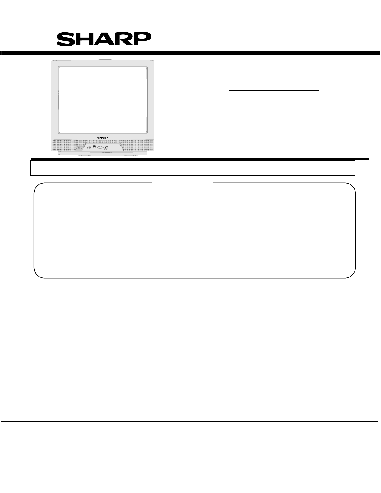
Sharp 21v-r70MM User manual

SERVICE MANUAL
21V-R70MM
COLOUR TELEVISION
Chassis No. GA6
21V-R70MM
In the interests of user safety (Required by safety regulations in some countries) the set should be restored to its original
condition and only parts indentical to those specified should be used.
S677421VR70MM
MODEL
ELECTRICAL SPECIFICATIONS
Chassis No. GA4
CONTENTS
IMPORTANT SERVICE SAFETY PRECAUTION ................................................................................................... 1-1
Page
LOCATION OF USER’S CONTROL ...................................................................................................................... 2-1
INSTALLATION AND SERVICE INSTRUCTIONS ................................................................................................. 3-1
SERVICE MODE ..................................................................................................................................................... 4-1
ADJUSTMENT METHOD ........................................................................................................................................ 5-1
WAVEFORMS ......................................................................................................................................................... 6-1
CHASSIS LAYOUT ................................................................................................................................................. 7-1
BLOCK DIAGRAM .................................................................................................................................................. 8-1
DESCRIPTION OF SCHEMATIC DIAGRAM .......................................................................................................... 9-1
SCHEMATIC DIAGRAMS ......................................................................................................................................10-1
PRINTED WIRING BOARD ASSEMBLIES ........................................................................................................... 11-1
Parts Guide
POWER INPUT............................AC 110-230 V, 50/60 Hz
POWER RATING .....................................................82W
PICTURE SIZE .............................1,239 cm2(192sq inch)
CONVERGENCE ............................................. Magnetic
SWEEP DEFLECTION .................................. .. Magnetic
FOCUS ........................................................ Electrostatic
INTERMEDIATE FREQUENCIES
Picture IF Carrier Frequency ...................... 45.75 MHz
Sound IF Carrier Frequency ...................... 41.25 MHz
Color Sub-Carrier Frequency ......................42.17 MHz
(Nominal)
AUDIO POWER
OUTPUT RATING... ...................... 3.0 W(RMS) x 1pc
SPEAKER
SIZE ........................................................ 2” X 3.5”, 1pc
VOICE COIL IMPEDANCE .................16 ohm at 400 Hz
ANTENNA INPUT IMPEDANCE
VHF/UHF ........................................75 ohm Unbalanced
TUNING RANGES
VHF-Channels ................................................. 2 thru 13
UHF-Channels ................................................14 thru 69
CATV Channels ............................................. 1 thru 125
(EIA, Channel Plan U.S.A.)
Specifications are subject to change without
prior notice.
SHARP CORPORATION This document has been published to be used for after
sales service only.
The contents are subject to change without notice.

21V-R70MM
1 – 1
TV21V-R70MMService Manual21V-R70MMMarketE
CHAPTER 1. IMPORTANT SERVICE SAFETY PRECAUTION
IMPORTANT SERVICE SAFETY PRECAUTION
Service work should be performed only by qualified service technicians who are
thoroughly familiar with all safety checks and the servicing guidelines which follow:
X-RADIATION AND HIGH VOLTAGE LIMITS
1. Be sure all service personnel are aware of the
procedures and instructions covering X-radiation.
The only potential source of X-ray in current solid
state TV receivers is the picture tube. However, the
picture tube does not emit measurable X-Ray
radiation, if the high voltage is as specified in the
"High Voltage Check" instructions.
It is only when high voltage is excessive that X-
radiation is capable of penetrating the shell of the
picture tube including the lead in the glass material.
The important precaution is to keep the high voltage
below the maximum level specified.
2. It is essential that servicemen have available at all
times an accurate high voltage meter.
The calibration of this meter should be checked
periodically.
3. High voltage should always be kept at the rated value
−no higher. Operation at higher voltages may cause
a failure of the picture tube or high voltage circuitry
and;also, under certain conditions, may produce
radiation in exceeding of desirable levels.
4. When the high voltage regulator is operating properly
there is no possibility of an X-radiation problem.
Every time a color chassis is serviced, the brightness
should be tested while monitoring the high voltage
with a meter to be certain that the high voltage does
not exceed the specified value and that it is regulating
correctly.
5. Do not use a picture tube other than that specified
or make unrecommended circuit modifications to the
high voltage circuitry.
6. When trouble shooting and taking test
measurements on a receiver with excessive high
voltage, avoid being unnecessarily close to the
receiver.
Do not operate the receiver longer than is necessary
to locate the cause of excessive voltage.
WARNING
1. For continued safety, no modification of any circuit
should be attempted.
2. Disconnect AC power before servicing.
3. Semiconductor heat sinks are potential shock
hazards when the chassis is operating.
4. The chassis in this receiver has two ground systems
which are separated by insulating material. The non-
isolated (hot) ground system is for the B+ voltage
regulator circuit and the horizontal output circuit. The
isolated ground system is for the low B+ DC voltages
and the secondary circuit of the high voltage
transformer.
To prevent electrical shock use an isolation
transformer between the line cord and power
receptacle, when servicing this chassis.
SERVICING OF HIGH VOLTAGE SYSTEM
AND PICTURE TUBE
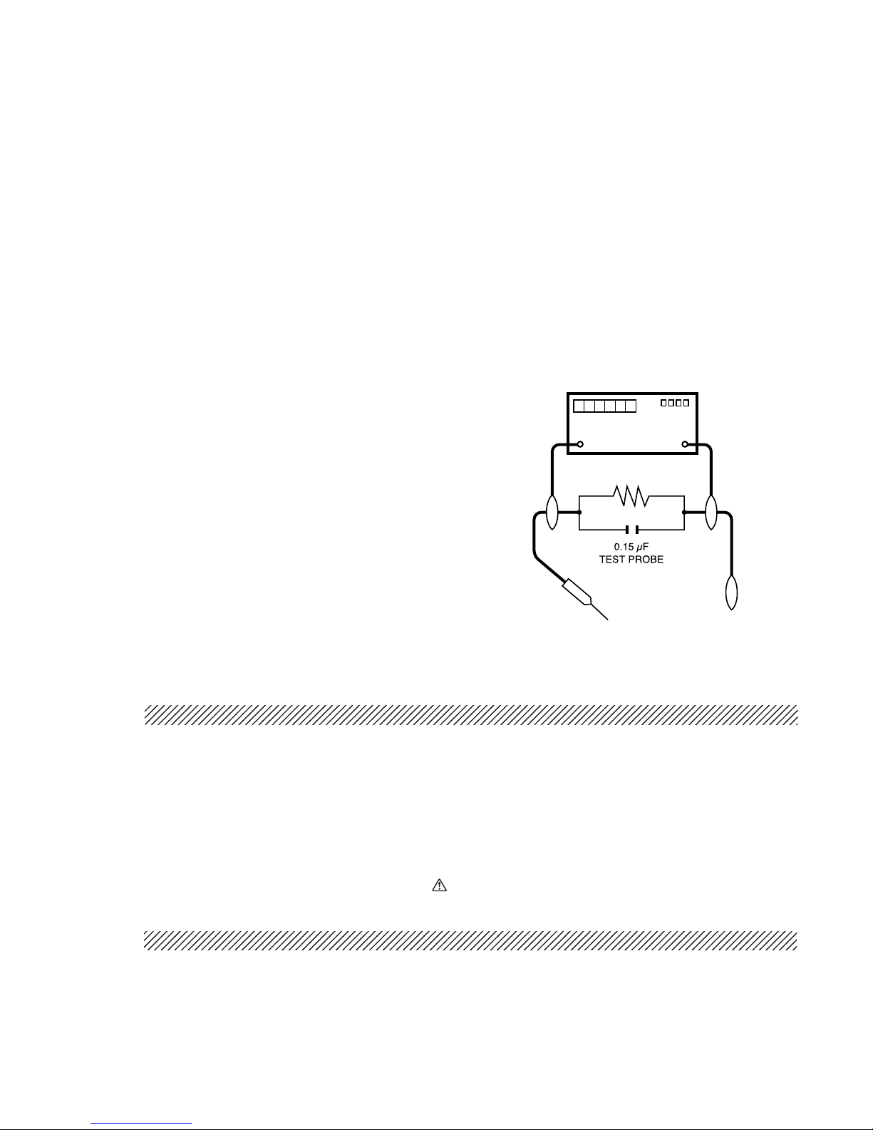
When servicing the high voltage system,
remove the static charge by connecting a
10k ohm resistor in series with an insulated
wire (such as a test probe) between the pic-
ture tube ground and the anode lead. (AC
line cord should be disconnected from AC
outlet.)
1. Picture tube in this receiver employs integral
implosion protection.
2. Replace with tube of the same type number for
continued safety.
3. Do not lift picture tube by the neck.
4. Handle the picture tube only when wearing
shatterproof goggles and after discharging the high
voltage anode completely.

21V-R70MM
1 – 2
SAFETY NOTICE
Many electrical and mechanical parts in television
receivers have special safety-related characteristics.
These characteristics are often not evident from visual
inspection, nor can protection afforded by them be
necessarily increased by using replacement components
rated for higher voltage, wattage, etc.
Replacement parts which have these special safety
characteristics are identified in this manual; electrical
components having such features are identified by " "
and shaded areas in the Replacement Parts Lists and
Schematic Diagrams.
IMPORTANT SERVICE SAFETY PRECAUTION
(Continued)
1. Inspect all lead dress to make certain that leads are
not pinched or that hardware is not lodged between
the chassis and other metal parts in the receiver.
2. Inspect all protective devices such as non-metallic
control knobs, insulating materials, cabinet backs,
adjustment and compartment covers or shields,
isolation resistor-capacity networks, mechanical
insulators, etc.
3. To be sure that no shock hazard exists, check for
leakage current in the following manner.
Plug the AC cord directly into a 110~230 volt AC
outlet, (Do not use an isolation transformer for this
test).
Using two clip leads, connect a 1.5k ohm, 10 watt
resistor paralleled by a 0.15µF capacitor in series
with all exposed metal cabinet parts and a known
earth ground, such as electrical conduit or electrical
ground connected to earth ground.
Use an AC voltmeter having with 5000 ohm per volt,
or higher, sensitivity to measure the AC voltage drop
across the resistor.
BEFORE RETURNING THE RECEIVER
(Fire & Shock Hazard)
Before returning the receiver to the user, perform
the following safety checks.
Connect the resistor connection to all exposed metal
parts having a return to the chassis (antenna, metal
cabinet, screw heads, knobs and control shafts,
escutcheon, etc.) and measure the AC voltage drop
across the resistor.
AII checks must be repeated with the AC line cord
plug connection reversed. (If necessary, a non-
polarized adapter plug must be used only for the
purpose of completing these check.)
Any current measured must not exceed 0.5 milliamp.
Any measurements not within the limits outlined
above indicate of a potential shock hazard and
corrective action must be taken before returning the
instrument to the customer.
For continued protection, replacement parts must be
identical to those used in the original circuit. The use of
substitute replacement parts which do not have the same
safety characteristics as the factory recommended
replacement parts shown in this service manual, may
create shock, fire, X-radiation or other hazards.
DVM
AC SCALE
1.5k ohm
10W
TO EXPOSED
METAL PARTS
CONNECT TO
KNOWN EARTH
GROUND
•
•
•
•

21V-R70MM
2 – 1
TV21V-R70MMService Manual21V-R70MMMarketE
CHAPTER 2. LOCATION OF USER'S CONTROL
[1] LOCATION OF USER'S CONTROL

21V-R70MM
3 – 1
TV21V-R70MMService Manual21V-R70MMMarketE
CHAPTER 3. INSTALLATION AND SERVICE INSTRUCTIONS
CIRCUIT PROTECTION
The receiver is protected by a 3.15A fuse (F701),
mounted on PWB-A, wired into one side of the AC
line input.
X-RADIATION PROTECTOR CIRCUIT TEST
After service has been performed on the horizontal
deflection system, high voltage system, B+ system,
test the X-Radiation protection circuit to ascertain
proper operation as follows:
1. Apply 110~230V AC using a variac transformer for
accurate input voltage.
2. Allow for warm up and adjust all customer controls
for normal picture and sound.
3. Receive a good local channel.
4. Connect a digital voltmeter to P603 pin3 and make
sure that the voltmeter reads 20 ±1.1V.
5. Apply external 27V DC at P603 pin3 by using an
external DC supply, TV must be shut off.
6. To reset the protector, unplug the AC cord and make
a short circuit between P603 pin1 and P603 pin2.
Now make sure that normal picture appears on the
screen.
7. If the operation of the horizontal oscillator does not
stop in step 5, the circuit must be repaired before the
set is returned to the customer.
HIGH VOLTAGE CHECK
High voltage is not adjustable but must be checked
to verify that the receiver is operating within safe
and efficient design limitations as specified checks
should be as follows:
1. Connect an accurate high voltage meter between
ground and anode of picture tube.
2. Operate receiver for at least 15 minutes at 110~230V
AC line voltage, with a strong air signal or a properly
tuned in test signal.
3. Enter the service mode and set Y-mute ON by using
Service R/C.
4. The voltage should be approximately 28.7kV (at zero
beam).
If a correct reading cannot be obtained, check circuitry
for malfunctioning components. After the voltage test,
make Y-mute off to the normal mode.
INSTALLATION AND SERVICE INSTRUCTIONS
Note: (1) When performing any adjustments to resistor controls and transformers use non-metallic
screwdrivers or TV alignment tools.
(2) Before performing adjustments, the TV set must be on at least 15 minutes.

21V-R70MM
4 – 1
TV21V-R70MMService Manual21V-R70MMMarketE
CHAPTER 4. SERVICE MODE
Service Mode Overview
1. Service mode is entered by SERVICE key input or CH-UP +VOL-DOWN input during reset.
2. Service mode is cleared by entering SERVICE key command during service mode.
3. If key input port (SERVICE) input is LOW, then it is in service mode.
4. During key input port (SERVICE) input is LOW, clearing service mode by key input SERVICE is disabled.
5. Service mode can be switched to 4 modes as follows by key input MENU;
SERVICE MODE
6. AFT processing is disabled during service mode. PLL setting data is set to fo data.
7. All user data are set to default during service mode. FAO and SPEAKER user settings are off and on respectively
in service mode. Energy Save is off.
8. Sleep timer, View timer, on timer and off timer are inactivated in Service mode.
9. Sound is muting in service mode except at Adjustment Items V20, M01, M03, M04, M05, and M06.
Adjustment mode
Setting mode First mode of service mode when SERVICE key is
pressed.
First mode of service mode when local key
CH-UP + VOL-DOWN is pressed after MCU reset.
Option mode
Check mode

21V-R70MM
4 – 2
Adjustment Mode Items
No. Item Name IC Register Range Default
V01 SUB-PICTURE 1 Chip CONTRAST 0~127 127
V02 SUB-TINT 1 Chip TINT 0~127 64
V03 SUB-COLOR 1 Chip COLOR 0~127 64
V04 SUB-BRIGHT 1 Chip BRIGHT 0~255 128
V05 SUB-SHARP 1 Chip VIDEO-TONE 0~63 32
V06 V-SHIFT 1 Chip V-SHIFT 0~7 4
V07 H-SHIFT 1 Chip H-PHASE 0~31 16
V08 RF-AGC 1 Chip RF-DELAY 0~127 127
V09 V-SIZE 1 Chip V-SIZE 0~63 32
V10 PIF-VCO 1 Chip VIF-VCO 0~63 32
V11 R-CUTOFF 1 Chip R-CUTOFF 0~255 127
V12 G-CUTOFF 1 Chip G-CUTOFF 0~255 127
V13 B-CUTOFF 1 Chip B-CUTOFF 0~255 127
V14 R-DRIVE 1 Chip R-DRIVE 0~127 64
V15 B-DRIVE 1 Chip B-DRIVE 0~127 64
V16 SUB-COLOR(YUV) 1 Chip COLOR 0~127 64
V17 SUB-TINT(YUV) 1 Chip BASEBAND-TINT 0~127 64
V18 CC-POS MICON CC-POS 0~255 32
V19 SCREEN CUT OFF 1 Chip CUT OFF 0~2 0
V20 SUB-VOL 1 Chip A-ATT 0~127 127
V21 H-VCO 1 Chip H-VCO 0~7 4
M01 MTS-ATT MTS ATT (MTS) 0~15 10
M02 MTS-VCO MTS VCO (MTS) 0~63 32
M03 MTS-FILTER MTS FILTER (MTS) 0~63 28
M04 MTS-WIDEBAND MTS WIDEBAND (MTS) 0~63 27
M05 MTS-SPECTRAL MTS SPECTRAL (MTS) 0~63 32
M06 SUB-VOL MTS VOL (MTS) 0~63 63

21V-R70MM
4 – 3
SELF ADJUSTMENT
H-VCO
1. When there is H-VCO self-adjustment key input for adjustment item H-VCO, self-adjustment is performed.
2. H-FREE(1chip) is set to 1.
3. H-OUT is set by intelligent monitor output.
4. IM input is set as TIM input.
5. H-VCO(1chip) data is changed so that the number of input pulse is 125 inside 8ms interval.
6. When adjustment completed, OSD display and H-VCO self-adjustment status data of EEPROM are updated.
7. H-FREE(1chip), intelligent monitor output and IM input mode are recovered.
RF-AGC
1. When there is RF-AGC self-adjustment key input for adjustment item RF-AGC, self-adjustment is performed.
2. AGC-OUT is set by intelligent monitor output.
3. IM input is set as AD input.
4. By decreasing RF-AGC (1chip) data from current RF-AGC adjustment value to 0, AFT input voltage becomes the
maximum setting value.
5. Increase RF-AGC(1chip) data, when AFT input voltage is at (max. 0.3V) point, adjustment is completed.
6. When adjustment completed, OSD display and RF-AGC self-adjustment status data of EEPROM are updated.
7. Intelligent monitor output and IM input mode are recovered.
PIF-VCO
1. When there is PIF-VCO self-adjustment key input for adjustment item PIF-VCO, self-adjustment is performed.
2. VIF-DEF(1chip) is set to 1.
3. AFC is set by intelligent monitor output.
4. IM input is set as AD input.
5. VIF-VCO(1chip) data is changed so that input voltage becomes 2.5V.
6. When adjustment completed, OSD display and PIF-VCO self-adjustment status data of EEPROM are updated.
7. VIF-DEF(1chip), intelligent monitor output and IM input mode are recovered.

21V-R70MM
4 – 4
Setting Mode Items
No. Item Name IC Register Range Default
F01 VIDEO TONE -GAIN (TV) 1 Chips V-TONE 0/1 0
F02 VIDEO TONE -GAIN (AV) 1 Chips V-TONE 0/1 0
F03
VIDEO TONE -GAIN (S-AV)
1 Chips V-TONE 0/1 0
F04 VIDEO TONE -GAIN(YUV) 1 Chips V-TONE 0/1 0
F05 ABCL 1 Chips ABCL 0/1 0
F06 BS 1 Chips BS-OFF 0/1 0
F07 ABCL-G 1 Chips ABCL-G 0/1 0
F08 SHP-AV OFFSET VIDEO-TONE(OFFSET) -16~+16 0
F09 SHP-SAV OFFSET VIDEO-TONE(OFFSET) -16~+16 0
F10 SHP-YUV OFFSET VIDEO-TONE(OFFSET) -16~+16 0
F11 RGB-CLIP 1 Chips EXTRGB-CLIP 0/1 0
F12 E-SAVE OFFSET CONTRAST(OFFSET) 0~63 30
F13 FAO-VOL 1 Chips A-ATT 0~127 120
F14 PIF-G 1 Chips VIF-GAIN 0~7 4
F15 Y-DELAY(TV) 1 Chips Y-DELAY 0~7 0
F16 Y-DELAY(AV) 1 Chips Y-DELAY 0~7 0
F17 Y-DELAY(SAV) 1 Chips Y-DELAY 0~7 0
F18 Y-DELAY(YUV) 1 Chips Y-DELAY 0~7 0
F19 TINT-AV OFFSET TINT(OFFSET) -32~+32 0
F20 TINT-SAV OFFSET TINT(OFFSET) -32~+32 0
F21 COL-AV OFFSET COLOR(OFFSET) -32~+32 0
F22 COL-SAV OFFSET COLOR(OFFSET) -32~+32 0
F23 R-DRI(R2) OFFSET R-DRI(OFFSET) -32~+32 0
F24 R-DRI( R) OFFSET R-DRI(OFFSET) -32~+32 0
F25 R-DRI(B) OFFSET R-DRI(OFFSET) -32~+32 0
F26 B-DRI(R2) OFFSET B-DRI(OFFSET) -32~+32 0
F27 B-DRI( R) OFFSET B-DRI(OFFSET) -32~+32 0
F28 B-DRI(B) OFFSET B-DRI(OFFSET) -32~+32 0
F29 V-FREE 1 Chips V-FREE 0/1 0
F30 GAMMA 1 Chips GAMMA 0~3 0
F31 TRAP(TV) 1 Chips TRAP-FINE 0~3 2
F32 TRAP(AV) 1 Chips TRAP-FINE 0~3 2
F33 H-FREE 1 Chips H-FREE 0/1 0
F34 1W(TV) 1 Chips V.WINDOW 0/1 0
F35 1W(AV) 1 Chips V.WINDOW 0/1 0
F36 YLPF 1 Chips YSW-LPF 0/1 1
F37 BS-D 1 Chips BS-DISCHARGE 0~3 0
F38 BS-C 1 Chips BS-CHARGE 0~3 0
F39 SL(TV) 1 Chips S-SLICE DOWN 0~3 0
F40 SL(AV) 1 Chips S-SLICE DOWN 0~3 0
F41 SL(SAV) 1 Chips S-SLICE DOWN 0~3 0
F42 SL(YUV) 1 Chips S-SLICE DOWN 0~3 0
F43 AFC2 1 Chips AFC2-G 0/1 0
F44 VD(TV) 1 Chips VSYNC-DET 0/1 0
F45 VD(AV) 1 Chips VSYNC-DET 0/1 0
F46 AS(TV) 1 Chips AUTO-SLICE 0/1 0
F47 AS(AV) 1 Chips AUTO-SLICE 0/1 0
F48 AS(SAV) 1 Chips AUTO-SLICE 0/1 0
F49 AS(YUV) 1 Chips AUTO-SLICE 0/1 0
F50 FBP(TV) 1 Chips FBP VTH 0/1 0
F51 FBP(AV) 1 Chips FBP VTH 0/1 0
F52 FBP(SAV) 1 Chips FBP VTH 0/1 0
F53 FBP(YUV) 1 Chips FBP VTH 0/1 0
F54 C.CLIP LEVEL 1 Chips C.CLIP LEVEL 0/1 0

21V-R70MM
4 – 5
Setting Mode Items (Continued)
No. Item Name IC Register Range Default
F55 PSW MTS PSW 0/1 0
F56 FAO-VOL MTS VOL 0~63 60
F57 CP PLL CHARGE PUMP 0/1 0
F58 CC LEVEL MICON CC LEVEL 0/1 0
F59 OSD POS MICON OSD POS 0/1 0
F60 OFFSET-ADJ-COL 1 Chips COLOR -32~+32 0
F61 OFFSET-ADJ-TINT 1 Chips TINT -32~+32 0
F62 OFFSET-ADJ-TINT-YUV 1 Chips BASEBAND-TINT -32~+32 0
F63 TIMER4-LOW SPEED 1 Chips TIMER4 VALUE 0~225 50
F64 TIMER4-HIGH SPEED 1 Chips TIMER4 VALUE 0~225 125
F65 R-CUT-YUV 1 Chips R-CUT(OFFSET) -63~+63 0
F66 G-CUT-YUV 1 Chips G-CUT(OFFSET) -63~+63 0
F67 B-CUT-YUV 1 Chips B-CUT(OFFSET) -63~+63 0
F68 R-DRI-YUV 1 Chips R-DRI(OFFSET) -63~+63 0
F69 B-DRI-YUV 1 Chips B-DRI(OFFSET) -63~+63 0
F70 CLOCK-ADJ 1 Chips 0~25 25

21V-R70MM
4 – 6
Option Mode Items
No OPTION FUNCTION 01
Default Data
001 DEMO Without DEMO With DEMO 1
002 DOWNLOAD Without V-CHIP OP With V-CHIP OP 0
003 V-CHIP Without V-CHIP With V-CHIP 0
004 SPEAKER Without SPEAKER With SPEAKER 1
005 FAO Without FAO With FAO 1
006 P.PREF Without P.REF With P.REF 1
007 UNIV+ Without UNIV+ With UNIV+ 1
008 VIEW TIMER Without VIEW TIMER With VIEW TIMER 1
009 EZ-SETUP EZ-SETUP AUTO PRESET 0
010 PON-CH Without POWER-ON With POWER-ON 0
011 FAV-COL FAV-COL COL-TEMP 1
012 COMPONENT Without COMPONENT With COMPONENT 1
013 AV Without AV With AV 1
014 AV2 AV1 system AV2 system 1
015 MTS Without MTS With MTS 1
016 TONE-CTRL Without S-ADJ With S-ADJ 1
017 AUTO-OFF Without AUTO-OFF With AUTO-OFF 1
018 INIT-LANG ENGLISH SPANISH 1
019 SETUP-FLAG NO SET UP AUTO SET UP 1
020 AV-FR
"0"=NO AV "1"=REAR "2"=FRONT "3"=REAR & FRONT
3
021 AV3/S-IN Without AV3/S-IN With AV3/S-IN 0
022 COMB Without COMB With COMB 0
023 AUTO-INPUT Without AUTO-INPUT With AUTO-INPUT 1
024 CLOCK Without CLOCK With CLOCK 1
025 LED SEMEX MODEL SPC MODEL 0
026 FLAT Not FLAT MODEL FLAT MODEL 1
027 BASS BOOST Without BASS BOOST With BASS BOOST 0
028 DSE Without DSE With DSE 0
029 SRS Without SRS With SRS 0
030 WHITE-OUT Without WHITE-OUT With WHITE-OUT 1
Check Mode
Micron mask version, software version and ROM correction function status are displayed in check mode.

21V-R70MM
5 – 1
TV21V-R70MMService Manual21V-R70MMMarketE
CHAPTER 5. ADJUSTMENT METHOD
Memory Map Data
Caution: to get into the service mode, one of the ways is press direct key for service items.
There is three stage of S ervice Mode data
Firststage data from V01 ~ M06
to go into second stage of service mode data, press MENU key
Second stage data from F01 ~ F70
to go into third s ta ge of s ervice mode da ta , pre s s ME N U ke y
Third stage data from O01 ~ O30
Below is the contents of these data
FirstStage
V01 C ONTR AS T 0~127 127 127
V02 TINT 0~127 64 54
V03 COLOR 0~127 64 35
V04 BR IGHT 0~255 128 127
V05 VIDEO-TONE 0~63 43 45
V06 V-SHIFT 0~7 4 2
V07 H-PHAS E 0~31 16 11
V08 R F-DE LAY 0~127 127 127
V09 V-SIZE 0~63 32 40
V10 VIF-VCO 0~63 32 32
V11 R -CUTOFF 0~255 127 127
V12 G-CUTOFF 0~255 127 127
V13 B-CUTOFF 0~255 127 127
V14 R -DR IVE 0~127 64 64
V15 B-DR IVE 0~127 64 64
V16 COLOR 0~127 64 64
V17 BAS E B AND-TINT 0~127 64 64
V18 CC-POS 0~255 32 32
V19 CUTOFF 0~2 0 0
V20 A-ATT 0~127 127 127
V21 H-VCO 0~7 4 4
M01 ATT (MTS ) 0~15 10 10
M02 VC O (MTS ) 0~63 32 32
M03 FILTE R (MTS ) 0~63 28 28
M04 W IDE B AND (MTS ) 0~63 27 27
M05 S P E C TR AL (MTS ) 0~63 32 32
M06 VOL (MTS ) 0~63 63 63
Auto Adjustment Item
1. H-VCO
2. R F-AGC
3. PIF-VCO
S e tting
Data
PIF-VCO
R-CUTOFF
G-CUTOFF
SUB-PICTURE
SUB-TINT
SUB-BRIGHT
SUB-COLOR
Service Mode
SUB-COLOR(YUV)
SCREEN CUTOFF
SUB-SHARP
V-SHIFT
H-SHIFT
RF-AGC
V-SIZE
B-CUTOFF
R-DRIVE
B-DRIVE
SUB-VOL
H-VCO
SUB-TINT(YUV)
CC-POS
MTS -ATT
MTS -VC O
MTS -F ILTE R
MTS -W IDE B AND
MTS -S P E C TR AL
SUB-VOL
Function Range Default
Data
Data

21V-R70MM
5 – 2
Second Stage
F01 V-TONE 0/1 0 0
F02 V-TONE 0/1 0 0
F03 V-TONE 0/1 0 0
F04 V-TONE 0/1 0 0
F05 ABCL 0/1 0 0
F06 BS-OFF 0/1 0 0
F07 ABCL-G 0/1 0 0
F08 VIDEO-TONE(OFFSET) -16~+16 0 0
F09 VIDEO-TONE(OFFSET) -16~+16 0 0
F10 VIDEO-TONE(OFFSET) -16~+16 0 0
F11 EXTRGB-CLIP 0/1 0 0
F12 CONTR AST(OFFSET) 0~63 30 30
F13 A-ATT 0~127 120 120
F14 VIF-GAIN 0~7 4 4
F15 Y-DELAY 0~7 0 5
F16 Y-DELAY 0~7 0 2
F17 Y-DELAY 0~7 0 0
F18 Y-DELAY 0~7 0 0
F19
T
INT(OFFS E T) -32~+32 0 -2
F20
T
INT(OFFS E T) -32~+32 0 0
F21 COLOR(OFFSET) -32~+32 0 +2
F22 COLOR(OFFSET) -32~+32 0 0
F23 R -DR I(OFFS E T) -32~+32 0 +8
F24 R -DR I(OFFS E T) -32~+32 0 +3
F25 R -DR I(OFFS E T) -32~+32 0 -2
F26 B -DR I(OFFS E T) -32~+32 0 -18
F27 B -DR I(OFFS E T) -32~+32 0 -8
F28 R -DR I(OFFS E T) -32~+32 0 +6
F29 V-FREE 0/1 0 0
F30 GAMMA 0~3 0 1
F31
T
RAP-FINE 0~3 2 2
F32
T
RAP-FINE 0~3 2 2
F33 H-FREE 0/1 0 0
F34 V.WINDOW 0/1 0 0
F35 V.WINDOW 0/1 0 1
F36 YSW-LPF 0/1 1 1
F37 BS-DISCHARGE 0~3 0 0
F38 BS-CHARGE 0~3 0 0
F39 S-SLICE DOWN 0~3 0 1
F40 S-SLICE DOWN 0~3 0 1
F41 S-SLICE DOWN 0~3 0 0
F42 S-SLICE DOWN 0~3 0 0
F43 AFC2-G 0/1 0 0
F44 VSYNC-DET 0/1 0 1
F45 VSYNC-DET 0/1 0 0
F46 AUTO-SLICE 0/1 0 1
F47 AUTO-SLICE 0/1 0 1
F48 AUTO-SLICE 0/1 0 0
F49 AUTO-SLICE 0/1 0 0
F50 FBP VTH 0/1 0 0
F51 FBP VTH 0/1 0 0
F52 FBP VTH 0/1 0 0
F53 FBP VTH 0/1 0 0
F54 C.CLIP LEVEL 0/1 0 0
F55 PSW 0/1 0 0
F56 VOL 0~63 60 58
F57 CHARGE PUMP 0/1 0 1
F58 CC LEVEL 0~31 0 0
F59 OSD POS 0/1 0 0
F60 COLOR -32~+32 0 +10
F61
T
INT -32~+32 0 +8
F62 BAS E BAND-TINT -32~+32 0 -12
F63
T
IME R 4 VALUE 0~255 50 50
F64
T
IME R 4 VALUE 0~255 125 125
OSD POS
OFFSET-ADJ-COL
Setting
Data
TINT-SAV
COL-AV
R-DRI(B)
SHP-SAV
SHP-YUV
TINT-AV
VIDEO-TONE-GAIN (AV)
VIDE O-T ONE -G AIN (S -AV)
VIDEO-TONE-GAIN (TV)
VIDEO-TONE-GAIN (YUV)
ABCL
BS
ABCL-G
RGB-CLIP
E-SAVE
FAO-VOL
SHP-AV
PIF-G
Y-DELAY(TV)
Y-DELAY(AV)
Y-DELAY(YUV)
Y-DELAY(SAV)
COL-SAV
R-DRI(R2)
B-DRI(R2)
B-DRI( R)
R-DRI( R)
R-DRI(B)
V-FREE
G AMMA
TRAP (TV)
TRAP (AV)
H-FR EE
1W(TV)
1W(AV)
YLPF
BS-D
BS-C
SL(TV)
SL(AV)
SL(SAV)
AFC2
VD(TV)
VD(AV)
SL(YUV)
AS (TV )
AS (AV)
AS (S AV)
AS (Y UV)
FBP(TV)
FBP(AV)
FBP(YUV)
C.CLIP LEVEL
FBP(SAV)
PSW
FAO-VOL
CP
CC LEVEL
OF FS E T-ADJ -TINT
OFFSET-ADJ-TINT-YUV
TIMER4-LOW SPEED
TIMER4-HIGH SPEED
Default
Data
Da ta S ervice Mode F unction R ange

21V-R70MM
5 – 3
F65 R -C UT(OF FS E T) -63~+63 0 0
F66 G-CUT(OFFSET) -63~+63 0 +36
F67 B-CUT(OFFSET) -63~+63 0 +2
F68 R -DR I(OFFS ET) -63~+63 0 0
F69 B-DR I(OFFS E T) -63~+63 0 0
F70 0~25 25 25
Third stage
O01 DEMO DISABLE ENABLE 1 1
O02 V-C HIP OP DIS ABLE E NABLE 0 0
O03 V-C HIP DIS ABLE E NABLE 0 0
O04 SPEAKE R DIS ABLE ENABLE 1 0
O05 FAO DISABLE ENABLE 1 0
O06 P.REF DISABLE ENABLE 1 0
O07 UNIV+ DISABLE ENABLE 1 0
O08 V IE W TIME R DIS AB LE E NAB LE 1 1
O09 EZ-SETUP AUTO PR ESET 0 0
O10 POWER -ON DISABLE ENABLE 0 1
O11 FAV-COL COL-TEMP 1 1
O12 COMPONENT DISABLE ENABLE 1 0
O13 AV DISABLE ENABLE 1 1
O14 AV1 AV2 1 0
O15 MTS DISABLE ENABLE 1 0
O16 S-ADJ DISABLE ENABLE 1 1
O17 AUTO-OFF DISABLE ENABLE 1 1
O18 ENGLISH SPANISH 1 1
O19 NO SET UP AUTO SET UP 1 0
O20 31
O21 AV3/S-IN DISABLE ENABLE 0 0
O22 COMB DISABLE ENABLE 0 0
O23 AUTO-INP UT DIS ABLE E NAB LE 1 0
O24 CLOCK DISABLE ENABLE 1 0
O25 SEMEX MODEL SPC MODEL 0 1
O26 FLAT DIS ABLE E NABLE 1 0
O27 BAS S BOOS T DIS ABLE E NABLE 0 0
O28 DSE DISABLE ENABLE 0 0
O29 SR S DISABLE ENABLE 0 0
O30 WHITE-OUT DISABLE ENABLE 1 0
*POWERONBYCH-UP/DOWNKEY.
S e tting
Data
"0"=NO AV "1"=R E AR "2"=F R O NT "3"=R E AR & F R ONT
B-DRI-YUV
CLOCK-ADJ
DOWNLOAD
DEMO
V-CHIP
SPEAKER
AUTO-OFF
AV
R-DRI-YUV
AV2
MTS
UNIV+
VIEW TIMER
TONE-CTR L
R-CUT-YUV
G-CUT-YUV
B-CUT-YUV
FAV-COL
COMPONENT
FAO
P.PREF
EZ-SETUP
*PON-CH
AV3/S -IN
COMB
AUTO-INPUT
INIT-LANG UAGE
SETUP-FLAG
AV-FR
DSE
SRS
WHITE-OUT
CLOCK
LED
FLAT
BASS BOOST
Data OPTION FUNCTION DATA = " 0" DATA =" 1" Default
Data

21V-R70MM
5 – 4
MODE L NAME
ADJ US TME NT
ITE M
ADJ US TME NT
POSITION
CONTROL
PRE-ADJUST
REQUIREMENT
CONTENT
INP UT
C ONDIT ION
OUTPUT
BUS OPTION FOR THIRD STAGE SERVICE DATA
FUNCTION O01 O02 O03 O04 O05 O06 O07 O08 O09 O10
DE MO DOWNL OAD V-C HIP S P FAO P .PR E F UNIV+ VIEW E Z P ON-C H
ADJUS TMENT 21V-R 70MM 1 0 0 0 0 0 0 1 0 1
PROCEDURE
DE F "0"= DISABLE
009 --> "0"= E Z-S E T UP "1"= AUT O P R E S E T
BUS OPTION FOR THIRD STAGE SERVICE DATA
FUNCTION O11 O12 O13 O14 O15 O16 O17 O18 O19 O20
FAV-C OL COMP AV AV2 MTS TONE AUTO
Init-LA NG
SETUP AV-FR
21V-R 70MM 1 0 1 0 0 1 1 1 0 1
FUNCTION O21 O22 O23 O24 O25 O26 O27 O28 O29 O30
AV3 C OMB A-IN C LOCK LE D FLAT BAS S DSE S R S W HIT E
21V-R 70MM 0 0 0 0 1 0 0 0 0 0
DE F O11 --> "0" =FAV-C OL "1"= C OL-TE MP
O18--> "0"= E NG LIS H "1" = S P ANIS H
O19--> "0"= NO SE T UP "1" = AUTO S ETUP
O20--> "0"=NO AV "1"=R E AR "2"=FR ONT "3"=R E AR &F R O NT
HIS TOR Y
OF R E VIS ION SYMBOL
21V-R 70MM
OPTION SET UP
STEP RANGE REFER AS BELOW
21V-R 70MM
OSD CHECKING
REVISED CONTENT .
"1"=ENABLE

21V-R70MM
5 – 5
MODE L NAME
ADJ US TME NT
ITE M
ADJ US TME NT
POSITION
CONTROL
PRE-ADJUST
REQUIREMENT
CONTENT
INP UT
CONDITION
OUTPUT
DATA SETUP FOR FIRST AND SECOND STAGE SERVICE DATA
V05 F15 F16 F 19 F21 F23 F 24 F 25 F26 F27
S HAR P Y-DL.T V Y-DL .AV T INT -AV C OL-AV R -D(R 2) R -D(R ) R -D(B) B-D(R 2) B-D(R )
ADJ US TME NT
PROCEDURE
F28 F30 F35 F39F40F44F46F47F56F57
B-D(B)
GAMMA
1W(AV) S L(TV) SL(AV) VD(TV) AS(TV) AS(AV)
FAO-VOL
CP
F60 F61 F62 F66 F67 F36
C-OF TINT-OF
TI-Y UV G -C -Y UV B -C -YU V
YLPF
DE F
SYMBOL
111
-2 -18 -82+8+345 5 2
+6
21V-R 70MM
21V-R 70MM
OSD CHECKING
HIS TOR Y
OF RE VIS ION REVISED CONTENT .
-2
1
21V-R 70MM
BUS SET UP
STEP RANGE REFER AS BELOW
58121V-R 70MM
-12 +36
11
FUNCTION
1
21V-R 70MM
+2 1+10 +8
FUNCTION
FUNCTION

21V-R70MM
5 – 6
ADJ US TME NT
ITE M
ADJ US TME NT
POSITION
CONTROL
PRE-ADJUST
REQUIREMENT
CONTENT
INP UT
CONDITION
OUTPUT
ADJUS TME NT
PROCEDURE
LEFT AND RIGHT SYMMETR ICAL
SYMBOL
I2C BUS CONTR OL
OPTION SET UP, BUS SE T UP,CR T-PURITY
MODE L NAME
H-POS ITION
STEP RANGEV07
21V-R 70MM
US 4 CH LION HEAD (MONOSCOPE)
AC 220V, US MAGNE T IC F IE LD
1.ADJ US T THE V07 BUS DATA TO HAVE A BALANCE P OS ITION TO S P E C OF A=B .
2.IFCANNOTMAKEITTOA=B,ADJFROMTHEBESTPOINTSOTHAT BSLIDELY
SMALLER THAN A
[CHECKING SPEC]
CONFIRMATION BY CRT SCREEN
HIS TOR Y
OF RE VIS ION REVISED CONTENT .
ı
ˇ

21V-R70MM
5 – 7
ADJ US TME NT
ITE M
ADJ US TME NT
POSITION
CONTROL
PRE-ADJUST
REQUIREMENT
CONTENT
INP UT
CONDITION
OUTPUT
ADJUS TME NT
PROCEDURE
SYMBOL
CONFIRMATION BY CRT SCREEN
ADJ US T THE V09 BUS DATA UNT ILL T HE OVE R S C AN B E COME AS S PE C IFIE D B E LOW .
C AUTION:- PLE AS E AG ING TV MOR E THAN 10 MINUT E S B E FOR E ADJUS TME NT.
[CHECKING SPEC]
OVER SCAN 10 ± 2.5%
I2C C ONTR OL
OPTION S ET UP, BUS S E T UP,CR T PUR ITY, V-PHASE , +B ADJUS T
US 4 CH LION HEAD
AC 220
MODE L NAME
V-SIZE
V09 STEP R ANGE
21V-R 70MM
HIS TOR Y
OF RE VIS ION REVISED CONTENT .

21V-R70MM
5 – 8
ADJ US TME NT
ITE M
ADJ US TME NT
POSITION
CONTROL
PRE-ADJUST
REQUIREMENT
CONTENT
INP UT
CONDITION
OUTPUT
ADJUS TME NT
PROCEDURE
SYMBOL
CONFIRMATION ON CRT SCREEN
ADJUST V06 BUS DATA TO HAVE A MOST ACCEPTABLE VERTICAL POSITION.
THE MONOS C OP E PATTE R N S HOULD BE BALANCE IN VE R TICAL POS ITION
NOTE: THE DATA FOR V06 LIMIT AT <= 04 , EVEN POSITION NOT GOOD ENOUGH
[C HE CK ING C ONFIR MAT ION ]
I2C CONTR OL
OPTION SET UP, BUS SET UP, CR T PURITY
US 4 CH LION HE AD (MONOS COPE P ATT ER N)
220 V, R F INP UT, ZE R O MAG NE TIC F IE LD
MODE L NAME
V-PHASE
V06 STEP R ANGE
21V-R 70MM
HIS TOR Y
OF RE VIS ION REVISED CONTENT .

21V-R70MM
5 – 9
ADJ US TME NT
ITE M
ADJ US TME NT
POSITION
CONTROL
PRE-ADJUST
REQUIREMENT
CONTENT
INP UT
CONDITION
OUTPUT
ADJUS TME NT
PROCEDURE
LEFT AND RIGHT SYMMETR ICAL.
SYMBOL
MODE L NAME
CLOSED CAPTION SET UP
V18 STEP RANGE 0 - 255
21V-R 70MM
CONFIRMATION ON CR T DISPLAY.
1)BY SELECTING THE V18, BOX BLK TEXT WILL BE APPEARED.
2)ADJ US T T HE V18 B US DAT A TO HAVE A B ALANC E P OS ITION T O S P E C OF A=B .
[CHECKING SPEC]
OPTION SET UP, BUS SE T UP
US 4 CH LION HEAD
AC 220
HIS TOR Y
OF RE VIS ION REVISED CONTENT .
ˇı
*REDUCE 5 STEPS AFTER ADJUSTED A=B
TEXT BOX BLK
Table of contents
Other Sharp TV manuals

Sharp
Sharp 28HW-53E User manual

Sharp
Sharp LC-32CHF5111E W User manual

Sharp
Sharp 32F543 XFlat User manual

Sharp
Sharp 15JF-25H User manual

Sharp
Sharp Aquos LC 26D4U User manual

Sharp
Sharp 32UF5 User manual

Sharp
Sharp 29E-S1F User manual

Sharp
Sharp LC-40FI5242KF Technical manual

Sharp
Sharp LC-32HI5012E User manual

Sharp
Sharp 21SFX10L User manual

Sharp
Sharp Aquos LC-32LE600E User manual

Sharp
Sharp cx68n5 User manual

Sharp
Sharp 50NP4 User manual

Sharp
Sharp 21K-FG1RU User manual

Sharp
Sharp 20AG1-SS User manual

Sharp
Sharp SX51LF7 User manual

Sharp
Sharp 32K-S400 User manual

Sharp
Sharp 25N S100 User manual

Sharp
Sharp 21LF-90N User manual

Sharp
Sharp 28LS-92EC User manual