Sharp DV-5145 User manual

SHARP
SERVICE
MANUAL
S85E7DV-51451
pE!
NEW COSMOS-3 CHASSIS
ARETUBE]
’
PAL
SYSTEM
COLOUR
TELEVISION
MODEL
DV-5145
In the interests of user-safety (Required by safety regulations in
some countries) the set should be restored to its original condition
and only parts identical to those specified should be used.
7
CoNTENTS
ELECTRICAL
SPECIFICATIONS
~
Page
.ELECTRICAL SPECIFICATIONS .............
1
.IMPORTANT SERVICE NOTES .............
2
l DESCRIPTION OF NEW CIRCUIT. ..........
3
.
SERVICE ADJUSTMENT
..................
.
TROUBLE SHOOTING TABLE
..............
,;
l
CHASSIS
LAYOUT
DIAGRAM
..............
15
.
PRINTED
WIRING
BOARD
ASSEMBLIES
......
17
l
BLOCK
DIAGRAMS
.....................
19
.
SCHEMATIC DIAGRAMS AND WAVEFORMS
...
21
l
REPLACEMENT PARTS
LIST.
..............
27
Aerial Input Impedance
..........
75 ohm unbalanced
Convergence
..............
Self Converging System
Focus
...............
High Bi-potential electrostatic
Audio Power Output Rating
..............
2W
max.
Intermediate Frequencies
Picture IF Frequency
..............36.875MHz
Sound Carrier Trap
................31.375MHz
Adjacent Sound Carrier Trap
.........38.375MHz
Powerlnput ...................
.240VAC50Hz
Power Consumption
......................80
W
Speaker
..........
5 cm x 9 cm Oval Dynamic x 1
pc.
Sweep Deflection
.....................
Magnetic
Tuning Ranges
............VHF
Channels
9
thru
11
UHF Channels 28 thru 63
Specifications
are
subject
to
change
without
prior notice.
-.
SHARP
CORPORATION
OF
AUSTRALIA
PlY
LTD.
Incorporated
in
Victoria
64-72
Seville
St., Fairfield. N.S.W.
2165,
Australia
Tel: (02)-728-9111

IMPORTANT
SERVICE
NOTES
Maintenance
and
repair
of
this receiver
should
be
done
by
qualified
service
personnel
only.
SERVICING
OF
HIGH
VOLTAGE
SYSTEM AND PICTURE
TUBE
When
servicing
the
high
voltage
system, remove static
charge
from
it
by
connecting
a
10k ohm
Resistor
in
series
with
an
insulated wire
(such
as
a
test
probe) between picture tube
tag
and
2nd anode
lead.
(AC
line
cord should
be
disconnected
from
AC
outlet.)
1.
Picture tube
in
this
receiver
employs integral implosion
protection.
2.
Replace
with tube
of
the
same
type number for continued safety.
3. Do not
lift
picture tube
by
the neck.
4.
Handle the picture tube only when wearing shatter-proof
goggles
and
after
discharging
the
high
voltage
completely.
X-RAY
This
receiver
is
designed
so
that
any
X-ray radiation
is
kept to
an
absolute
minimum.
Since
certain
malfunctions
or
servicing
may
pro-
duce
potentially
hazardous
rediation with prolonged exposure
at
close
range,
the
following
precautions should
be
observed:
1:
When repairing the circuit,
be
sure
not
to
increase
the
high
voltage
to
more the
28kV,
(at
beam
1
.l
mA),
for
the
set.
2.
To
keep
the
set
in
a
normal
operation,
be
sure
to make it function
on
25.0kV
+
1.5
kV
(at
beam
1.2
mA)
in
the
case
of
the
set.
The
set
has
been
factory-adjusted
to
the above-mentioned
high
voltage.
’
.
.
If
there
is
a
possibility
that
the
high
voltage
fluctuates
as
a
result
of the
repairs,
never
forget
to
check
for
such
high
voltage
after
the work.
3. Do not substitute
a
picture tube
with
unauthorized types
and/or
brands
which may
cause
excess
X-ray radiation.
BEFORE
RETURNING
THE
RECEIVER
Before returning the
receiver
to
the
user,
perform
the
following
safety
checks.
1.
Inspect
all
lead
dress
to
make certain
that
leads
are
not pinched or
that
hardware
is
not lodged between the
chassis
and
other metal
parts
in
the
receiver.
2. Inspect
all
protective
devices
such
as
non-metallic
control knobs,
insulating fishpapers, cabinet
backs,
adjustment
and
compartment
covers
or
shields,
isolation resistor-capacity networks, mechinical
insulators
etc.
2

DESCRIPTION
OF
NEW
CIRCUIT
ICl
01
RH-iX0605CEZZ (MICRO
PROCESSOR)
1. Outline of
IClOl
(1) IClOl consists of ROM (1270 words x 8 bits) and
RAM (32 words x 4 bits).
(2) Presetting of the described stations allowed by
operating the TUNING
(+)I(-)
keys and FINE TUN-
ING
(+)/(-)
keys.
(3) Tuning voltage available in 16,384 steps due to D/A
output.
(4) Channel number display by
2-digit
7-segment LED.
(5) Display of 11 ch. to 16ch. is allowed by using “10”
key in combination with one of “1” to “6” keys.
2. Pins arrangement of IClOl and its external connec-
tion
3.
Key
matrix
Table l-l
Eo
El
E2
E3
I
Fo
/
F,
/
F2
’
:
F3
j
F4
I
10
i
I
4
/
8
’
/
FT(+)
1
5
9
!
1
FT(-)
6
!
2
’
T(+)
I
3
/
7
//
T(-)
F”
ICI101
rt.
~~~-wlOUTP"T
J
VI)‘
-
-
22
t-4
21
F5
4L
~+$&-j
E.
vss
*+5v
CLOCK
vGG
--
-30~
20
Fe
VHF
’
’
::&f”’
lc3
IL,
BAND
OUTPl
JT
c
AFT
MUTE
-
SOUND
MUTE
Figure l-l
4. Sweeping
speed
of
tuning
key
Table l-3
Tyew
/
I
TUNING
(+)I(-)
FINE
TUNING
(+)I(-)
/
/
Resolution Sweeping
speed
,
Reso,ution
Sweeping
speed
within
a
band
1
within
a
band
3 min
VHF-L
10sec
/,
VHF-H
8116,384
20
set
!
2/16,384
I
6
min
UHF
1
/
I
/
40
set
I
12
min
Table 1-2
1
I
I
C
E/
E
1
1
I
E2
I
-
I
3

5. Key operation at each mode
Key
1
-
10
T(+)
V-1
F-n+)
m-1
10
Normal mode
Preset mode
When one of “1” to “10” keys is pushed, the data
of the corresponding position is read out of the
memory so that the desired station is tuned in.
The currently selected station is stored as lastly
selected position in the memory.
When one of “1
fl
to “10” keys is pushed, the
corresponding position is displayed on LED. But
the data in the memory remains as it is.
Not operative.
When FT(+) or
FT(-)
key is pushed, APT is turned
off and the unit performs a sweeping of tuning
voltage. And when the key is touched off, the data
of tuning voltage is written in the memory.
Within 2 seconds after “10” key has been pushed,
when one of “I” to “6” keys is pushed, one of
“11“
to “16” positions is displayed and tuned in;
when one of “7” to “IO” keys is, however,
pushed, one of
“7”
to “10” positions is displayed
and tuned in.
t
1
When
T(+)
or
T(-
key is pushed, the unit performs
a sweeping of tuning voltage. And when the key is
touched off, the data of tuning voltage is written in
the memory.
When FT(+) or
FT(-)
key is pushed, the unit
performs a sweeping of tuning voltage. And when
the key is touched off, the data of tuning voltage is
written in the memon/.
Within 2 seconds after “10” key has been pushed,
when one of “1” to “6” keys is pushed, one of
“11” to “16” positions is displayed but not tuned
in since the data in the memory is kept as it is.
6. Tuning operation
When one of “1” to “IO” keys is pushed in the normal
mode, the corresponding data is read out of the EA
ROM so that the band output and tuning voltage are set
up to allow the unit to tune in the desired station. Then
the currently tuned in station is stored as a lastly
selected position in the specified address of EA ROM.
During the tuning operation, AFT output and MUTE
output are caused in the following timing.
AFT
output
(AI)
11
I
I
MUTE
output
*
I
I
MO)
Writing /Reading
l
of
last
pf
tuninq
I
I
data voltage
i”
’
ata
Ii
1
II
I
1
50-60
i’-
50
msec
16
msec
1
200
msec
msec
‘1
0
AFT
turns
on
when
AFI
output
is
at
High
level.
l
Muting
occurs
when
MUTE
output
is
at
High
level.
Figure 1-2

IC203
RH-iXO6OlCEZZ
(PIF/SIF/JUNGLE)
1. Outline of
IC203
(1)
(2)
(3)
(4)
(5)
(6)
(7)
(8)
(9)
(10)
(11)
PIF amplifier of sync demodulator type
Negative modulation AGC detector circuit
Tuner RF
AGUIF
AGC
AFC circuit
Video preamplifier
Sound IF amplifier and demodulator circuit
Horizontal oscillator drive circuit/horizontal oscilla-
tor/horizontal output circuit
Audio preamplifier
Horizontal sync circuit with two control loops
Sawtooth wave generator/vertical sync circuit with
50Hz/60Hz
automatic
verfical
amplitude control cir-
cuit
Sand castle pulse generator circuit
2. Pins arrangement
AGC
TAKEOVER
RAMP
GENERATOR
VERTICAL
DRIVE
VERTICAL
FEEDBACK
TUNER
AGC
GROUND
SUPPLY
(+B)
IF
INPUT
IF
INPUT
DECOUPLING
CAPACITOR
VOLUME
CONTROL
AUDIO
OUTPUT
SOUND
DEMODULATOR
SOUND
IF
DECOUPLING
Figure 2-l.
3. Function
PHASE-U
DETECTOR
(APC)
SAND
CASTLE
HORIZONTAL
DRIVE
SYNCSEPARATOR
FREQUENCY
CONTROL
HORIZONTAL
OSCILLATOR
COINCIDENCE
DETECTOR
SYNC
DEMODULATOR
SYNC
DEMODULATOR
AGC
DETECTOR
AFT
VIDEO
OUTPUT
GROUND
SOUND
IF
INPUT
Pin
0:
AGC cut-in level
Pin
0:
Generation of vertical sawtooth wave
Pin
0:
Vertical drive output
Pin
@:
Vertical feedback circuit (correction of vertical
linearity and size)
Pin
0:
Tuner RF AGC
Pin
@:
PIF ground
Pin
0:
Power supply + B (1 IV)
Pin
@:
IF input
Pin
@:
IF input
Pin
@I:
IF decoupling capacitor
Pin
0:
Sound volume control
Pin
0:
Audio output
Pin
0:
SIF detection
Pin
@:
SIF decoupling capacitor
Pin
0:
SIF input
Pin
@:
SIF.horizontal
oscillator ground
Pin
0:
Video output
Pin
@:
AFT
Pin
@:
AGC detector
Pin
@I:
IF sync detector circuit
Pin
@I:
IF sync detector circuit
Pin
@:
Sync circuit
Pin
@I:
Pin
@:
Pin
@:
Pin
@:
Pin
@:
I
1
I
I
1
II
f
1
/
$/ith
no;
*
/
-I
Fast’
’
Slow
1
Field
intensity
Sync
stgnal
flow
’I
-
’
Fast
-cI
Slow
y
Figure 2-2.
Horizontal oscillator circuit
AFC circuit (1st control loop for frequency con-
trol)
Sync separator circuit (to decide sync separa-
tion level)
Horizontal drive output circuit (also works as
horizontal drive pulse input circuit.)
Sand castle output
Resulted
from
FBT
pulse
and
sync
signal
made
together
Figure 2-3.
l
This
output
is
used
for
the
following
functions;
@
Burst
samPling.
@
Blanking,
@
DC
restoration
and
@
Flip-flop
Pin
@:
Phase-II detector (APC circuit 2nd control loop
for phase control)
5

IC501
RH-iX0640CEZZ
(VERTICAL
OUTPUT)
1. Outline of
IC501
(I) High output
(2) Lower power consumption thanks to the built-in
4. Circuitry
bhaviors
(I) The vertical oscillation signal entering pin @of
pump up circuit
(3) The number of external parts reduced
2. Pins arrangement
,
VERTICAL
DRIVE
4
4
5
F”
K+
-
IAJX
-s
>o,
I
2
1
--d
1
-io-o~o?j,+j-
g
.k
5
-
.g
.g
2
3
0
s
a
-2s
s
sf
-
+
5
2
;:
-
c”
tij
>
0
E
P
3
iG
2
&
.z
5
.z
r
%a
m
;
E
f
F
8
o>
5:
3
z
0
2
lC501
activates the vertical drive circuit and vertical
output circuit.
(2
)
When the vertical drive circuit and vertical output
circuit are in action, it is only in the
flyback
period
that the booster (pump up) circuit is allowed to
operate to provide the voltage about twice
Vcc.
(3
I) The design that the supply voltage is boosted only
in the
flyback
period results in remarkably reduced
power consumption.
(4) In the c
onventional
SRPP output circuit,
Vcc
must
be supplied until the
flyback
pulse voltage reaches
its highest value. In this circuit, however, it is
sufficient to use about half of Vcc for the circuitry
operation.
Figure 3-1.
3. Block diagram and application
DC.
NF
B
0
D.Y
+BI
AC.
NF
B
JVP-P
INPUT
Figure 3-2.
6

IC701
RH-iX0689CEZZ
(POWER
REGULATOR)
1. Oscillation principle
(1) When the power switch is turned on, a current
IsI
is
applied to the base of TR5.
(2) Then, a current lc=hfe.ls, is applied to the collector
of TR5.
(3) The current
lc
available at the collector of TR5
causes a voltage (feedback voltage of the same
polarity) at
T701.
(4) As the feedback voltage is given, a current
IF
available at pin @of
l701
is allowed to run through
0705 and R711 and enter the base of TR5. When the
feedback voltage increases to more than the speci-
fied level, TR5 starts its oscillation.
(5) As the voltage at the collector of TR5 increases to
its saturation point, a reverse bias is applied to its
base to interrupt the oscillation.
(6) When the oscillation of TR5 is stopped, the energy
stored in
T701
is discharged through the secondary
winding N4.
(7) Then there is caused a voltage (of the reverse
polarity) at
Nl
and N2 to turn on TR5 again.
Thereafter, the process is repeated for TR5 to
perform the oscillation continuously.
2. Operational principle of error amplifier
(1) The voltage which is induced at N3 winding is DC
rectified to produce a control voltage (between pins
@and
0).
The control voltage available at N3 is highly correla-
tive with the output voltage of N4 because both N3
and N4 are electrically coupled with each other.
(2) Variation of the control voltage is detected by TRl
and
ZDl.
(3) As the detec e voltage increases, it is amplified by
t d
TR2 and TR3 so that the current at the base of TR5
is bypassed.
(4) Then the current at the collector of TR5
is
limited to
the smallest.
(5) Accordingly, the pulse width is controlled to decide
the duration where TR5 is kept turned on.
3. Over-current protector circuit
(1) An over-current
12
is applied to TR4. With TR4
turned on, the current at the base of TR5 is so
reduced that TR5 will eventually stop the oscillation.
(2) With the over-current applied to TR5, there
is
caused
a
voltage
between
pins@and@of
T701
and
this
voltage
is
supplied
via
0705
and
R711
to
the
base
of
TR5,
so
that
Vin
DC
is
allowed to
run
in
C708
and
R708
to
enter the
base
of
TR5.
In
the actual
circuitry,
however,
this
current
Vin
DC can’t
reach
the
base
of
TR5
because
that
C708
has
already
been
charged
up.
h31
0
11
N.C
R3 =
*
TRl
1
1
u
Figure 4.
D2
7
+B

IC801
RH-iX0603CEZZ (VIDEO/CHROMA)
1. Outline of
MO1
1)
PAL signal demodulation and R/G/B matrix output
2) White peak limiter control circuit 3) R/G/B mixing circuit included
4) Sand castle pulse processor
2. Pins arrangement
+12V
POWER
SUPPLY
CONTROL
VOLTAGE
FOR
INDENTIFICATION
CHROMINANCE
INPUT
REFERENCE
VOLTAGE
A.C.C
DETECTOR
CONTROL
VOLTAGE
A.C.C
SATURATION
CONTROL
CONTRAST
CONTROL
SANDCASTLE
AND
FIELD
BLANKING
INPUT
VIDEO
DATA
SWITCHING
LUMINANCE
SIGNAL
INPUT
BRIGHTNESS
CONTROL
RED
OUTPUT
(INPUT
OF
EXTERNAL
RED)
GREEN
OUTPUT
Figure 5.
3. Circuitry behaviors
Pin
0:
12V power supply
Pin
0:
Generation of ACC detector control voltage
(generation of killer on/off control voltage)
Pin
0:
Chroma input
Pin
@:
Reference voltage for ACC detector
Pin
0:
ACC control voltage
The peak detector ACC works to detect the
voltage which is proportional to the burst signal
level.
Pin
@:
Colour saturation control
Pin
0:
Contrast control
Pin
@:
Sand castle puise input
The sand castle pulse is divided into two pulses;
the first pulse is set at
1.5V
DC and used for
blanking of the
R/G/B
output signal, and the
second pulse is set at
7.OV
DC and used for
black level clamping and burst keying.
Pin
@:
Video data switching
Switching between R/G/B input and video input
is performed:
R/G/B
input at High level, video
input at Low level.
Pin
@I:
Luminance signal input
Pin
0:
Brightness control
Pin
0:
Red output
Pin
8:
Input of external red
Pin
@I:
Green output
Pin
@:
Input of external green
Pin
@I:
Blue output
Pin
0:
Input of external blue
Pin
0:
Pin
@I:
Pin
@:
Black level clamping (only with R/G/B signal
input) to provide the same black level in both
R/G/B input mode and video mode.
Pin
0:
B-Y input demodulator
Pin
@I:
R-Y input demodulator
Pin
@:
Burst phase detector output
Pin
@:
1
These are used to compare the burst gate
signal with the reference signal coming from
the reference oscillator, so that the resultant
signal in applied to the external low pass filter
(R804, C818) to produce a phase control vol-
tage.
Pin @
Pin
@:
1
Reference oscillator
8.86 MHz of the reference oscillator is halved
to be 4.43 MHz (this makes esier a 90” phase
shift operation).
Pin
@I:
Ground
)
OUTPUT
OF
THE
CHROMA
AMPLIFIER
I
GROUND
REFERENCE
OSCILLATOR
I
REFERENCE
OSCILLATOR
BURST
PHASE
DETECTOR
OUTPUT
’
BURST
PHASE
DETECTOR
OUTPUT
R-Y
INPUT
DEMODULATOR
1
B-Y
INPUT
DEMODULATOR
BLACK
LEVEL
CLAMP
CAPACITOR
BLACK
LEVEL
CLAMP
CAPACITOR
I
BLACK
LEVEL
CLAMP
CAPACITOR
(INPUT
OF
EXTERNAL
BLUE)
)
BLUE
OUTPUT
)
(INPUT
OF
EXTERNAL
GREEN)
Pin
@I:
Chroma output

SERVICE
ADJUSTMENT
Precautions:
How to prevent
ICs
from damages due to static elec-
tricity
1.
2.
3.
4
When replacing or handling the IC, be sure to put on
your wrist a metal ring (earth ring) that is connected
to ground.
+
Avoid touching the IC directly by hand as much as
possible.
For the soldering iron and other jigs in use, be sure
to connect them to ground so that their potential is
the same as that of the PWB and/or IC.
The PWB cannot be connected to ground in some
condition although you attempt to attach the IC to
that PWB. In this case, be sure to keep the PWB at the
same potential as ground by touching it by your
hand on which a metal ring
is
put.
When handling the IC, it
is
recommended for you to
wear such clothes as not causing static electricity;
the ones of wool, silk or synthetic fiber should be
avoided. This is important in particular when hand-
ling the IC in a dry environment.
Overall waveform
1.
2.
3.
4.
Receive 10 ch. signal.
Connect the sweep output to the tuner TP (test point)
through the specified jig.
Connect the response lead to TP403.
l Oscilloscope range: 0.2V/cm
Connect a resistor (100 ohms) to both ends of R229
(10
kohms)
and short
C,.
Note: Keep the lead of the 100 ohm resistor as short
as possible.
A
Shorting
__
L
--=
J
T201
(P-DET)
5. Apply DC voltage (about 5V) TP207 (IF-AGC) and
adjust so that the output waveform on oscilloscope is
at
O.GVp-p.
Note: The voltage applied to TP207 should not ex-
ceed 7V in any case.
6. Check that the overall waveform is within the speci-
fied range shown below.
‘\il’
C:
-8
f
2.5
dB
P:
-6
?I
2.5
dB
If the waveform is out of the specified range, adjust it by
using the IF transformer (IFT) on the tuner.
n Location of TP and
IFT
of the tuner:
Adjustment of AFT:
T201
1.
2.
3.
4.
5.
6,
Receive luminance-order colour bar signal.
Adjust R225 (RF-AGC control) so that normal picture
appears on TV
screen.
(Set the band switch at NORMAL position.)
Connect
36.875
MHz
oscillator to
TP204
across
a
capacitor
of
1
pF.
Connect oscilloscope to TP403.
l Oscilloscope range: 0.5 V/cm AC
l Sync operation: Horizontal
Adjust the oscillator’s output so that signal beating
is
observed on oscilloscope.
Adjust the tuning control to have zero beating on
oscilloscope as shown in the figure below.
(Set the band switch at VHF position.)
6
Zero
beating
7. Set the band switch at NORMAL position and adjust
T201 to make zero the beating.
r
[1
Adjusting
point
T201
9

RF AGC cut-in adjustment:
RZ25
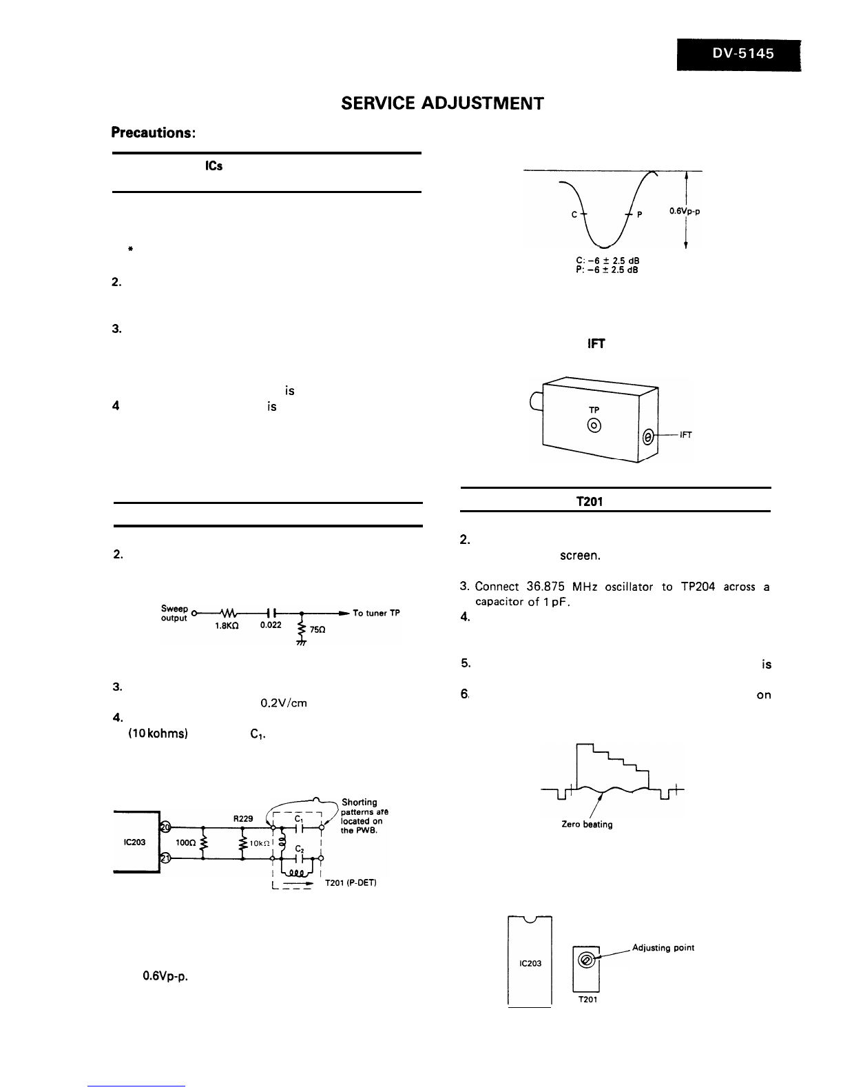
1. Receive 10 ch. signal.
2. Set the signal input level at 52 +1
dBu.
3. Connect CR oscillator to TP202 across a capacitor of
10
uF/lGV:
This capacitor is to cut off DC supply.
I
aIsl2.L
ToTP202
c
r
-,
r.
I
-
To TP201
l Oscillation frequency: 1
kHz
sine wave
l Output voltage : 0.1 vp-p
(when connected to TP202)
4. Adjust R225 so that 1
kHz
signal disappears from TV
screen.
5. Set the signal input level at
52+3
dBp
and check that
1
kHz
signal appears on TV screen.
If 1
kHz
signal does not appear, set the input signal
level at 52
dBu
again and follow the procedure in
step 4 again.
Sound detector coil adjustment:
T301
1. Connect signal generator’s output to TP301.
l Generator’s central frequency: 5.5 MHz
l Modulation: No modulation
l Generator output: 80
dBu
(terminated with
50R)
2. Connect DC voltmeter to TP302.
3. Adjust sound volume to minimum and measure the
voltage then available at TP302; this voltage (about
2.5V)
should be regarded as a reference voltage.
4. Adjust sound volume to maximum and turn the core
of T301 (sound detector coil) until DC voltmeter reads
the reference voltage obtained in step 3 above.
Horizontal
frequency
adjustment: R605
1. Receive monoscope pattern signal.
2. Short TP601 and TP602 (at both ends of
R606).
3. Adjust R605 to obtain good horizontal sync on
TV
screen.
4. Remove the short-circuit between TP601 and TP602.
Sub-brightness adjustment: R415
1. Short TP401 and TP402.
2. Set each control as follows:
l Screen control: at MIN position
l G-bias control
(R853-A):
at MIN position
l B-bias control
(R853-B):
at MIN position
l R-bias control (R869): at MIN position
l G-drive control
(R854-A):
at CENTER position
l B-drive control
(R854-B):
at CENTER position
l
Contrast control (R 1110) : at M IN position
l Brightness control
(Rl
110): at CENTER position
l
Picture control
(R
1110) : at CENTER position
l Colour control
(Rl
110) : at MIN position.
3. Receive monoscope pattern signal.
4. Connect oscilloscope to TP850 (with L2 connected to
ground)
5. Adjust
R415
(sub-brightness control) so that the
output waveform on oscilloscope is at 15 Vp-p.
6. Remove the short-circuit between TP401 and
TP402.
Background adjustment:
R854-A;
G-drive control,
R853-A;
G-bias control
R854-B;
B-drive control,
R853-B;
B-bias control
Screen control, R869; R-bias control
1. Receive monoscope pattern signal.
2. Set each control as follows:
l Brightness control: at CENTER position
l Contrast control: at MIN position
l Screen control: at MIN position
l G-, B-drive controls: at CENTER position
l R-, G-, B-bias controls: at MIN position
3. Short
TP401
and TP402.
4. Turn screen control until horizontal raster slightly
appears on TV screen.
5. One of the colours (R, G and B) appears first as
screen control is turned. So touching off the bias
control belonging to the first colour, adjust the other
controls as follows to make white the horizontal
raster.
I
First
/
colour
1
Bias controls to be next turned.
I
Red
I
R853-A,
R853-B
I
Green
1
R869, R853-B
I
Blue
1
R869,
B853-A
6. Turn screen control until the raster disappears and
stop it.
7. Remove the short-circuit between TP401 and TP402.
8. Set contrast control at MAX position.
10

9. Adjust each drive control for good white balance.
l Colour temperature:
7300°K
I
x
=
0.303
y
=
0.310
1
10. Adjust brightness control and contrast control to
obtain a dark picture, then follow the procedure in
step 5 to make white the raster.
11. Again brighten the picture and adjust each drive
control for good white balance as in step 9 above.
1H
delay line adjustment: R806,
T802
1.
2.
3.
4.
5.
6.
Receive colour bar signal.
Set each control as follows:
l Brightness control: at CENTER position
l Colour control: at CENTER position
Connect oscilloscope to TP851 (collector of Q852) on
CRT PWB (with L2 grounded).
l Sync operation: Horizontal
Note:
The probe
of
oscilloscope
in
use
must
be
of a low
capacitance (2 to 3
pF).
Adjust contrast control so that the top of output
waveform on oscilloscope won’t be depressed.
Short TP401 and TP402.
Adjust R806 and T802 so that the parts “A” and “B”
shown below become minimum respectively.
waveform after
adjustment
Horizontal size adjustment:
S601
1. Receive monoscope pattern signal.
2. If the horizontal size is at less than 7% of
overscan-
ning, insert the socket into the opening (2) of
SSOl.
(1)
(2)
H-SIZE
Horizontal center adjustment: R618
1. Adjust
R618
to have proper horizontal center.
Vertical size adjustment: R508
1. Adjust
R508
to have the vertical size be at 8% of
overscanning.
Vertical center adjustment:
S501
1. If the vertical center of picture is 5 mm higher than
the geometrical center
of
CRT, set
S501
at “down”
position.
If it is 5 mm lower than the geometrical
center
of
CRT,
set
S501
at “up” position.
D
+5 mm or
more
$
t
-5
mm or
more
-
downh
APC adjustment: R802
Protector check
1. Receive luminance-order colour bar signal.
2. Short TP803 and TP804, and also TP801 and TP802.
4. Remove the short-circuits between
TP803
and T804,
3. Adjust R802 so that barber pole pattern appears on
and between TP801 and TP802.
lV
screen.
1. Apply DC 22V to TP703
(0
side of
C728),
and check
that the protector remains inoperative.
3. Connect a resistor of 10 kohms between TP704 (base
2. Apply DC 28V to TP703, and check that the protector
of Q703) and ground, and check that the protector
gets operative.
gets operative.
Sub colour adjustment: R817 Sub-sound adjustment: R4008
1. Receive luminance-order colour bar signal.
l Signal input level: 80
dBp
_+
5
dBp
2. Set each control as follows:
l Brightness control: at CENTER position
l Contrast control: at MAX position
l Colour control: at CENTER position
l Picture tone control: at CENTER position
3. Connect oscilloscope to TP850 (collector of
Q850)
(with L2 grounded).
4. Adjust
R817
(sub colour control) so that the white
output (75%) and red output will have the same level.
11
1.
Receive
an
audio
signal
of
400
Hz
and
30%
modulation.
2. Connect a dummy
resistor
of
8ohms to the
speaker
terminal.
3. Set sound volume
(R
1111)
at
MAX
position.
4. Connect
an
effective-value voltmeter to the
dummy
resistor.
.
5.
Adjust
R4008
(Sub-sound
control)
so
that
the
output
voltage
of
the dummy
resistor
is
3.35
Vms.

TROUBLE
SHOOTING
TABLE
I
NO
RASTER
I
No
I
15V
line
is normal?
No
1
I
Check D701
-
704,
D706, D708, T701,
L706,
IC701 and
F7001
115V
line
is normal?
I
25V line No
Yes
is normal?
_
.
)‘r’<;>~’
Check Q702,
.,
Check D502, 0711,
1
R741,
T701 and
115 V line.
R725
Waveform at
base of 0601
No
1
4
Check R724,
I
YCS
I
Q701, Q703,
D710 and
D716.
I
Check
IC203.
I
I
No
,
Check R617
and T602.
Yes
c
.I
+
((HI-4 terminal)
No
Check D709
and R732.
@;gi;;;&>
No I
Waveform at
YCS
TP403 is
normal?
No I
I
1
I
)I
Check
IC203,
Q401
and A/V Unit.
Check IC801
12

I
NO
COLOUR
I
I
No
I
YOS
Check
IC801.
I
I I
No
I
I
1
I
Check
RlllOand
R817.
I
I
Check
IC801.
I
NO
PICTURE
.
I
YIK
Check
IC801,
RlOOl,
Q40
1
and
Video
Switch
Unit.
I
Check
Q850,0851
and
Q852.
IC203,
Q203
and
Tuner.
13

Waveform at
No
Check
IC203.
No
,
w
w
1
@c,k
IC501
andCheck L501.
I.
I
NO
SOUND
Yes
Check
IC201,
0301
and
IClOl.
Waveform at
Yes
c
4
No
I,
Check
IC301.
1
1
.
.
I
Check SP301,
J3001 and
L301.
I
14

CHASSIS
LAYOUT
I
LEn
Uhi
d
DUNTKI,
74WE
SK
UNIT
DUNTK4175WE
/
.
CRT
VI301
VBA5iJAA95XOi
CRT
UNIT
DUNTK
418BWE
,
II
I
CONTROL
UNJT
L
DUNTK4173WE
SPEAKER
Sp301
j
;;DNETo,;AF;;E
UNJT
1
~OT~J;Z
REAR VIEW
HEAD
PHONE
UNIT
DUNTK4176WE
H-CENT
u
~~
-;601]j
OIiOI
m
-
TP202
0
IC203
T201 L601
IF)
no
CF401
Ill
Il-
II
lC2Ol
u
n
+.
0203
0401 l
u
/I/
r-
H-SIZE
cc-all,
T301
-
II
1
u
T:302
7f”‘$30,
,
~c501
0
TPZO?
01
%:
=y--J(
n
lC3
(Tf)
YJNER
0
TP2OI
ISA)
II
“f$iR7&\,
f
u
IGJ
’
c
d
R701
cl
c
XC701
-
(Al
C706
OL
R707
L
0
,
/
T701
D
0
c719
1

R853-A
G-
BIAS
R853-8
8-BIAS
R
Dl201
VIDEO
I
D1(08)
AA2
0
0
AAI
(AB)
I
1
%P
T2A
0
A3
.
Al
(SD)
v
c4049
-
0
ki?
04010
0
CSO)U
0401
I
0
C4008
04009
l0
04007
l
0
04008
0
04006
(OJ)
04005
0
rl
IC4001
I
I
rJ
(0)
El
I?4008
SUB
SOUND
IC4004
I
I
IC4003
(01)
0
I
I
DUNTK4172WE
J40Ol J4003
J4002
,
/
h
11.
AB3
0
ABI
0
s7001
.
J3OOl
(TA) (TB)
T
01107
5Cl-l
6CH
7CH
8CH
9CH
IOCH
SllO5 SllO6 SllO7 SllO8 Silo9
SlllOl
SIIII
Slll2
S1113
S1114
q
~aiollollollollol~m
SllOl
FINE-TUNE
(+I,
St103
TUNE
(+I
I
7
I
8
I
9
I
10
I
11
I
12
I
16

PRINTED
WIRING
BOARD
ASSEMBLIES
(All
the
PWBs
here
are
shown
an
viewed
from their
wiring
sides.)
J-l
z
-4
I
f
1
r
I
z
C
G
\
,
I/p’“’
$
J”
-l-l
-Jl
I
lo”
k(j
LCA
:,
N
::
t
703
M
R701
D-/O,
u
ft
-
702
CA
L706
c7cJ-l
-.
-+
D
ow
jl
2:
:+;
4
I-
P--R
ma-
-C6!5-
tI
i
3
4
56
kl
r
4’
+
E
Mother Unit
A
B
CRT Socket Unit
1
1
2
1
3
1
4
I
6
I
6
I
17

ao3-
L
A/V
Unit
-7
07-
7
01107
-7,
oz-
-0
16
El
lx-
yJa
k-
-_l.t,tl;I
”
--my
1
QPWEJF4174CEZZ/
LED Unit
[QPWBFOI
75CEZZ
]
oi
EO
Power Switch Unit
--R3002-
-
3002
u
N
[QPWBF4176CEZZ]
Earphone Jack Unit
-
._
(OPW8F41’3‘EZZ
_
(Ta),
LEln5-
*‘J
-
5
3
DUNTK4173WE
g,
5
-n/1
fj
-
;+:,by,”
6
F&’
’
‘ml,\-]
3
/
c
101 31
2’
CCYTQAST
+c-
PlC’“W
6
d
51
01
<,,I-1
5
c.
%
-
i;O
pq-yijyf~E.q
$J
-*q=y
9
21115 51116
-
2-
-7(lT)=
1SAN0
5E
i
ECT
5.v
Control Unit
6
I
7
I
8
I
9
I
10
I
11
I
12
18

-
G
Hi
E
a
a
s
E
Y
0
9
m
r
-:
%F
v)x
*-
-I
*-
E
1
t
0
---
I
I
I
3,
I
I
I
I
I
I
I
I
I
I
3
I
I
‘A
L
I1I
2
I
3
I
4
I
5
I
6
I
7
19

3
-Ii
g;;
fnnf
e-
-3
I*-
1
\
1
‘I
>
)
>
0
e-m
3:
I
II
I
I
I I
I
I
?I
!I
I
L-J
IL
I
l-
-da
:
G
5
1
2
k
s
1
I
?
~&&le3&E!3&&&&c5ezld5&
8
0
------7
G
0000000000000000000000000000
;;
I
I
2
E
ti 0”
0
0
;
z
Fi
r-
0
z
z
0
Z
N
0
P
;;o
0,
,,
ii
=
ii
In
=
:
u-l E-l
Z
==
m
ii
Gl
u)
Z
=
I
’
5
ii
v,
Gi
’
@-IO
0,
L---------
__-----_-----------------------------------~-------------,
a
z;o’
33 0:
-
=I
I--------ml---
---’
>
-II
’
OQI
+--Do~~
lr7l-II
-c=I
t;
;;;
OP
t
z
-cI
2
2
5
I-
’
31
5
5
3
”
ii
J
--------
s
2
zz
a
I
7
I
8
I
9
I
10
I
11
I
12
I
20
Table of contents
Other Sharp TV manuals

Sharp
Sharp Aquos LC 37D64U User manual

Sharp
Sharp 32HW-57EDE User manual

Sharp
Sharp 21V1-L User manual

Sharp
Sharp Aquos LC-46D82U User manual

Sharp
Sharp LC-48CFG6001K User manual

Sharp
Sharp LC32DV24U - 31.5" LCD TV User manual

Sharp
Sharp Aquos LC-60LE830E User manual

Sharp
Sharp 27C540 User manual

Sharp
Sharp 27F540 User manual

Sharp
Sharp LC-32BD6X User manual

Sharp
Sharp 50DJ1K User manual

Sharp
Sharp Aquos LC 32D50U User manual

Sharp
Sharp 66GS-62H User manual

Sharp
Sharp Aquos LC-108D1U User manual

Sharp
Sharp 32JW-74EES User manual

Sharp
Sharp 21YF30 User manual

Sharp
Sharp 27R-S480 User manual

Sharp
Sharp 20AG2-SMK3 User manual

Sharp
Sharp 37GT-25S User manual

Sharp
Sharp 32JF-74E User manual