SIGNALCORE SC5317A User manual


©2018 Rev 1.1
1
General Information
Table of Contents
1General Information..............................................................................................................................4
Warranty .......................................................................................................................................4
Copyright & Trademarks................................................................................................................4
International Materials Declarations.............................................................................................5
CE European Union EMC & Safety Compliance Declaration..........................................................5
Warnings Regarding Use of SignalCore Products ..........................................................................5
2Physical Description...............................................................................................................................6
Unpacking......................................................................................................................................6
Setting Up the Device....................................................................................................................6
Front Interface Indicators and Connectors....................................................................................7
Signal Connections ................................................................................................................7
Device LED Indicators ............................................................................................................7
Communication and Supply Connection ...............................................................................8
Mini-USB Connection ............................................................................................................9
Reset Button (Pin Hole) .........................................................................................................9
3Functional Description...........................................................................................................................9
Overview .......................................................................................................................................9
The Signal Chain ..........................................................................................................................10
The RF Input ........................................................................................................................10
The Input Path Switch..........................................................................................................11
The RF Path..........................................................................................................................11
The First Mixer and IF Path..................................................................................................12
Signal Chain Configurations.................................................................................................12
The LO Synthesizer and External Ports........................................................................................13
The Reference Clocks ..........................................................................................................13
LO Ports...............................................................................................................................14
The Interface Module..................................................................................................................14
4Hardware Registers .............................................................................................................................14
Configuration Registers ...............................................................................................................14
Register 0x02 SET_SYS_ACTIVE ...........................................................................................15
Register 0x03 SYTHN_MODE (2 Bytes) ................................................................................16
Register 0x10 RF_FREQUENCY ............................................................................................16
Rev 1.1 | SC5317A & SC5318A Hardware Manual SignalCore, Inc.
2
SC5317A & SC5318A Hardware Manual
Register 0x11 IF_FREQUENCY..............................................................................................17
Register 0x12 LO_FREQUENCY ............................................................................................17
Register 0x14 RF_AMP ........................................................................................................17
Register 0x15 ATTENUATOR................................................................................................18
Register 0x16 SIGNAL_PATH................................................................................................18
Register 0x18 STORE_DEFAULT_STATE ...............................................................................19
Register 0x19 DEVICE_STANDBY .........................................................................................19
Register 0x1A REFERENCE_CLOCK.......................................................................................20
Register 0x1B REFERENCE_DAC...........................................................................................20
Register 0x1C USER_EEPROM_WRITE.................................................................................20
Register 0x1F SYNTH_SELF_CAL ..........................................................................................21
Query Registers ...........................................................................................................................21
Register 0x30 GET_DEVICE_PARAM....................................................................................22
Register 0x31 GET_TEMPERATURE .....................................................................................22
Register 0x32 GET_DEVICE_STATUS....................................................................................23
Register 0x33 GET_DEVICE_INFO........................................................................................24
Register 0x34 CAL_EEPROM_READ .....................................................................................24
Register 0x35 USER_EEPROM_READ...................................................................................25
Register 0x36 SERIAL_OUT_BUFFER....................................................................................25
Device Parameters Data and Format...................................................................................25
Device Information Parameters and Format.......................................................................26
5Communication Interfaces ....................................................................................................................1
Communication Data Format ........................................................................................................1
USB Interface................................................................................................................................. 1
Control Transfer ....................................................................................................................1
Bulk Transfer .........................................................................................................................1
SPI Interface ..................................................................................................................................2
Writing the SPI Bus................................................................................................................3
Reading the SPI Bus...............................................................................................................3
RS232 Interface .............................................................................................................................4
Writing to the Device Via RS232............................................................................................4
Reading from the Device Via RS232 ......................................................................................5
PXI .................................................................................................................................................5

©2018 Rev 1.1
3
General Information
Setting Up the PCI to Serial Bridge ........................................................................................5
Writing to the Device.............................................................................................................5
Reading from the Device .......................................................................................................6
6Calibration.............................................................................................................................................6
Calibration EEPROM Map..............................................................................................................6
Absolute Conversion Gain .............................................................................................................7
Absolute Gain of the RF Conversion Path......................................................................................8
Gain Through the Bypass RF Conversion Path...............................................................................8
Applying Calibration ..............................................................................................................8
Revision Table..............................................................................................................................................10

Rev 1.1 | SC5317A & SC5318A Hardware Manual SignalCore, Inc.
4
SC5317A & SC5318A Hardware Manual
1General Information
Warranty
This product is warranted against defects in materials and workmanship for a period of one year from
the date of shipment. SignalCore will, at its option, repair or replace equipment that proves to be
defective during the warranty period. This warranty includes parts and labor.
Before any equipment will be accepted for warranty repair or replacement, a Return Material
Authorization (RMA) number must be obtained from a SignalCore customer service representative and
clearly marked on the outside of the return package. SignalCore will pay all shipping costs relating to
warranty repair or replacement.
SignalCore strives to make the information in this document as accurate as possible. The document has
been carefully reviewed for technical and typographic accuracy. If technical or typographical errors
exist, SignalCore reserves the right to make changes to subsequent editions of this document without
prior notice to possessors of this edition. Please contact SignalCore if errors are suspected. In no event
shall SignalCore be liable for any damages arising out of or related to this document or the information
contained in it.
EXCEPT AS SPECIFIED HEREIN, SIGNALCORE, INCORPORATED MAKES NO WARRANTIES, EXPRESS OR
IMPLIED, AND SPECIFICALLY DISCLAIMS ANY WARRANTY OF MERCHANTABILITY OR FITNESS FOR A
PARTICULAR PURPOSE. CUSTOMER’S RIGHT TO RECOVER DAMAGES CAUSED BY FAULT OR NEGLIGENCE
ON THE PART OF SIGNALCORE, INCORPORATED SHALL BE LIMITED TO THE AMOUNT THERETOFORE PAID
BY THE CUSTOMER. SIGNALCORE, INCORPORATED WILL NOT BE LIABLE FOR DAMAGES RESULTING FROM
LOSS OF DATA, PROFITS, USE OF PRODUCTS, OR INCIDENTAL OR CONSEQUENTIAL DAMAGES, EVEN IF
ADVISED OF THE POSSIBILITY THEREOF. This limitation of the liability of SignalCore, Incorporated will
apply regardless of the form of action, whether in contract or tort, including negligence. Any action
against SignalCore, Incorporated must be brought within one year after the cause of action accrues.
SignalCore, Incorporated shall not be liable for any delay in performance due to causes beyond its
reasonable control. The warranty provided herein does not cover damages, defects, malfunctions, or
service failures caused by owner’s failure to follow SignalCore, Incorporated’s installation, operation, or
maintenance instructions; owner’s modification of the product; owner’s abuse, misuse, or negligent
acts; and power failure or surges, fire, flood, accident, actions of third parties, or other events outside
reasonable control.
Copyright & Trademarks
Under the copyright laws, this publication may not be reproduced or transmitted in any form, electronic
or mechanical, including photocopying, recording, storing in an information retrieval system, or
translating, in whole or in part, without the prior written consent of SignalCore, Incorporated.
SignalCore, Incorporated respects the intellectual property rights of others, and we ask those who use
our products to do the same. Copyright and other intellectual property laws protect our products. Use
of SignalCore products is restricted to applications that do not infringe on the intellectual property rights
of others.

©2018 Rev 1.1
5
General Information
“SignalCore”, “signalcore.com”, and the phrase “preserving signal integrity” are registered trademarks
of SignalCore, Incorporated. Other product and company names mentioned herein are trademarks or
trade names of their respective companies.
International Materials Declarations
SignalCore, Incorporated uses a fully RoHS compliant manufacturing process for our products.
Therefore, SignalCore hereby declares that its products do not contain restricted materials as defined
by European Union directive 2002/95/EC (EU RoHS) in any amounts higher than limits stated in the
directive. This statement assumes reliable information and data provided by our component suppliers
and may not have been independently verified through other means. For products sold into China, we
also comply with the “Administrative Measure on the Control of Pollution Caused by Electronic
Information Products” (China RoHS). In the current stage of this legislation, the content of six hazardous
materials must be explicitly declared. Each of those materials, and the categorical amount present in
our products, are shown below:
鉛
Lead
(Pb)
汞
Mercury
(Hg)
镉
Cadmium
(Cd)
六价铬
Hexavalent
Chromium
(Cr(VI))
多溴联苯
Polybrominated
biphenyls
(PBB)
多溴二苯醚
Polybrominated
diphenyl ethers
(PBDE)
✓
✓
✓
✓
✓
✓
A ✓indicates that the hazardous substance contained in all of the homogeneous materials for this
product is below the limit requirement in SJ/T11363-2006. An Xindicates that the particular hazardous
substance contained in at least one of the homogeneous materials used for this product is above the
limit requirement in SJ/T11363-2006.
CE European Union EMC & Safety Compliance Declaration
The European Conformity (CE) marking is affixed to products with input of 50 - 1,000 Vac or 75 - 1,500
Vdc and/or for products which may cause or be affected by electromagnetic disturbance. The CE
marking symbolizes conformity of the product with the applicable requirements. CE compliance is a
manufacturer’s self-declaration allowing products to circulate freely within the European Union (EU).
SignalCore products meet the essential requirements of Directives 2004/108/EC (EMC) and 2006/95/EC
(product safety) and comply with the relevant standards. Standards for Measurement, Control and
Laboratory Equipment include EN 61326 and EN 55011 for EMC, and EN 61010-1 for product safety.
Warnings Regarding Use of SignalCore Products
(1)
PRODUCTS FOR SALE BY SIGNALCORE, INCORPORATED ARE NOT DESIGNED WITH COMPONENTS NOR TESTED
FOR A LEVEL OF RELIABILITY SUITABLE FOR USE IN OR IN CONNECTION WITH SURGICAL IMPLANTS OR AS
CRITICAL COMPONENTS IN ANY LIFE SUPPORT SYSTEMS WHOSE FAILURE TO PERFORM CAN REASONABLY BE
EXPECTED TO CAUSE SIGNIFICANT INJURY TO A HUMAN.
Rev 1.1 | SC5317A & SC5318A Hardware Manual SignalCore, Inc.
6
SC5317A & SC5318A Hardware Manual
(2)
IN ANY APPLICATION, INCLUDING THE ABOVE, RELIABILITY OF OPERATION OF THE SOFTWARE PRODUCTS CAN
BE IMPAIRED BY ADVERSE FACTORS, INCLUDING BUT NOT LIMITED TO FLUCTUATIONS IN ELECTRICAL POWER
SUPPLY, COMPUTER HARDWARE MALFUNCTIONS, COMPUTER OPERATING SYSTEM SOFTWARE FITNESS,
FITNESS OF COMPILERS AND DEVELOPMENT SOFTWARE USED TO DEVELOP AN APPLICATION, INSTALLATION
ERRORS, SOFTWARE AND HARDWARE COMPATIBILITY PROBLEMS, MALFUNCTIONS OR FAILURES OF
ELECTRONIC MONITORING OR CONTROL DEVICES, TRANSIENT FAILURES OF ELECTRONIC SYSTEMS
(HARDWARE AND/OR SOFTWARE), UNANTICIPATED USES OR MISUSES, OR ERRORS ON THE PART OF THE USER
OR APPLICATIONS DESIGNER (ADVERSE FACTORS SUCH AS THESE ARE HEREAFTER COLLECTIVELY TERMED
“SYSTEM FAILURES”). ANY APPLICATION WHERE A SYSTEM FAILURE WOULD CREATE A RISK OF HARM TO
PROPERTY OR PERSONS (INCLUDING THE RISK OF BODILY INJURY AND DEATH) SHOULD NOT BE SOLELY
RELIANT UPON ANY ONE COMPONENT DUE TO THE RISK OF SYSTEM FAILURE. TO AVOID DAMAGE, INJURY,
OR DEATH, THE USER OR APPLICATION DESIGNER MUST TAKE REASONABLY PRUDENT STEPS TO PROTECT
AGAINST SYSTEM FAILURES, INCLUDING BUT NOT LIMITED TO BACK-UP OR SHUT DOWN MECHANISMS.
BECAUSE EACH END-USER SYSTEM IS CUSTOMIZED AND DIFFERS FROM SIGNALCORE'S TESTING PLATFORMS,
AND BECAUSE A USER OR APPLICATION DESIGNER MAY USE SIGNALCORE PRODUCTS IN COMBINATION WITH
OTHER PRODUCTS IN A MANNER NOT EVALUATED OR CONTEMPLATED BY SIGNALCORE, THE USER OR
APPLICATION DESIGNER IS ULTIMATELY RESPONSIBLE FOR VERIFYING AND VALIDATING THE SUITABILITY OF
SIGNALCORE PRODUCTS WHENEVER SIGNALCORE PRODUCTS ARE INCORPORATED IN A SYSTEM OR
APPLICATION, INCLUDING, WITHOUT LIMITATION, THE APPROPRIATE DESIGN, PROCESS AND SAFETY LEVEL
OF SUCH SYSTEM OR APPLICATION.
2Physical Description
Unpacking
All SignalCore products ship in antistatic packaging (bags) to prevent damage from electrostatic discharge
(ESD). Under certain conditions, an ESD event can instantly and permanently damage several of the
components found in SignalCore products. Therefore, to avoid damage when handling any SignalCore
hardware, you must take the following precautions:
1. Ground yourself using a grounding strap or by touching a grounded metal object.
2. Touch the antistatic bag to a grounded metal object before removing the hardware from
its packaging.
3. NEVER touch exposed signal pins. Due to the inherent performance degradation caused
by ESD protection circuits in the RF path, the device has minimal ESD protection against
direct injection of ESD into the RF signal pins.
4. When not in use, store all SignalCore products in their original antistatic bags.
Remove the product from its packaging and inspect it for loose components or any signs of damage. Notify
SignalCore immediately if the product appears damaged in any way.
Setting Up the Device
Integration of the SC5317A and SC5318A modules requires attention to maintain effective cooling.
Inadequate cooling can cause the temperature inside the RF housing to rise above the maximum for this
product, leading to improper performance, reduction of product lifespan or complete product failure.
SignalCore suggests providing either moderate airflow across the RF housing, or if active cooling is not an
option, using thermal interface materials to bond the RF housing to a larger heatsinking surface (i.e. a
system enclosure). As each system configuration into which the device is integrated is unique, detailed
cooling options cannot be provided.

©2018 Rev 1.1
7
Physical Description
A cooling plan is sufficient when the SC5317A and SC5318A on-board temperature sensors indicate a rise
of no more than 20°C above ambient temperature under normal operating conditions.
Front Interface Indicators and Connectors
The SC5317A is a PXIe-based RF downconverter with all user I/O located on the front face of the module.
The SC5318A is a serial controlled core module, whose front face connections are shown in Figure 1.
Signal Connections
All signal connections (ports) on the device are female SMA-type. Exercise caution when fastening cables
to the signal connections. Over-tightening any connection can cause permanent damage to the device.
The condition of your system signal connections can significantly affect measurement accuracy and
repeatability. Improperly mated connections or dirty, damaged, or worn connectors can degrade
measurement performance. Clean out any loose, dry debris from connectors with clean, low-
pressure air (available in spray cans from office supply stores).
If deeper cleaning is necessary, use lint-free swabs and isopropyl alcohol to gently clean inside the
connector barrel and the external threads. Do not mate connectors until the alcohol has completely
evaporated. Excess liquid alcohol trapped inside the connector may take several days to fully
evaporate and may degrade measurement performance until fully evaporated.
Tighten all SMA connections to 8.8 in-lb max (100 N-cm max)
RF In
This is the RF input port to the device with nominal impedance
of 50 . Its maximum input power is +27 dBm.
RF out
This is the bypass output port of the RF input signal with
nominal impedance of 50 .
IF out
This is the IF output of the device with nominal impedance of
50 .
LO/Ref In
This is the 10 MHz refence input to the device, enabling the
device to phase lock its internal clocks to an external reference
source. This nominally 50 port is AC coupled. This port is also
shared with the device external LO input. Maximum rated
input power is +10 dBm for both Ref and LO signals.
LO rear
This is the other selectable external LO input port. Only one LO
port, either the front or rear, is selected as the input.
Device LED Indicators
These are LED indicator lights for the device, and their functions are listed in Table 1 and Table 2.
Rev 1.1 | SC5317A & SC5318A Hardware Manual SignalCore, Inc.
8
SC5317A & SC5318A Hardware Manual
Table 1. Status LED Indicator
LED Color
Description
Green
The device is functioning properly in the state that it is programmed for.
Amber
Indicates that all functions are on standby mode.
Red
Indicates that one or more local oscillators are not functioning correctly.
Off
No supply or supply error
Table 2. Active Indicator
LED Color
Description
Green
An external interface port has accessed the device.
Red
Input supply voltage exceeded
Off
No current interface access
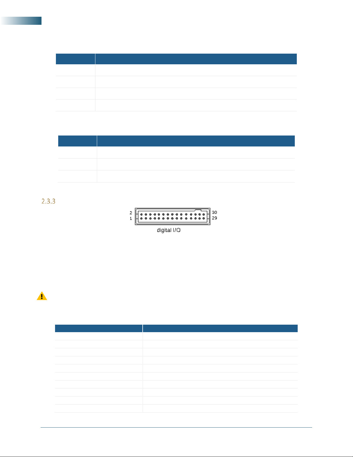
Communication and Supply Connection
Figure 1. Power and Digital IO Connector
Power and communication to the SC5318A is provided through a a rectangular connector from Samtec
whose part number is TFM-115-01-L-D-RA. It also serves as the digital connector interface for RS232/SPI,
trigger, and other digital signals. A mating pig-tail cable, part number SFSD-15-28-H-10.00-SR, is provided
with the product. The pin definitions are listed in Table 3.
Pinouts are different for different SignalCore products with the same connector type. Please ensure
that mating connectors and cables are wired correctly before connection.
Table 3. Interface connector pin out description
PIN #
Description
22,24,26,28,30
12V Supply Rail
3,7,11,15,19,21,23,25,27,29
GND
13,14,16,17,19
Reserved, Do Not Connect
2
RX for RS232 or MISO for SPI (Host referred)
4
TX for RS232 or MOSI for SPI (Host referred)
5
SPI CLK
6
SPI CS_b
8
RS232 Baud Rate / SPI Mode Select
9
Device status
10
Device active
©2018 Rev 1.1
9
Functional Description
12
System Reset, Logic 0 to Reset Device
18
Reserved, Pull High to 3.3V or DNC
20
SRDY. This pin is serial ready for SPI
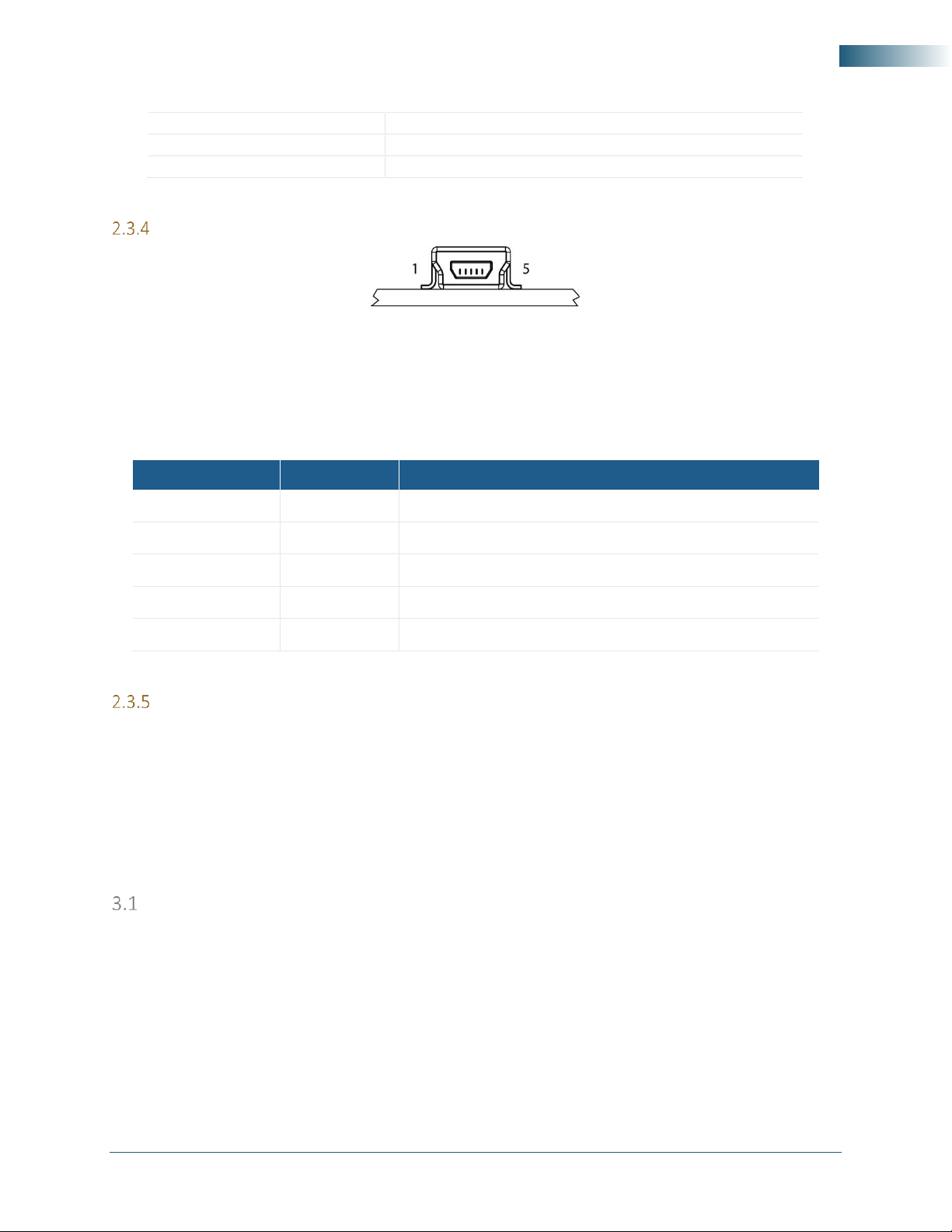
Mini-USB Connection
This is a mini-USB Type B connector for USB communication with the device using the standard USB 2.0
protocol (full speed) found on most host computers. The pinout of this connector, viewed from the front,
is shown in the following table.
PIN #
USB Function
Description
1
VBUS
Vcc (+5 Volts)
2
D-
Serial Data (neg)
3
D+
Serial Data (pos)
4
ID
Not Used
5
GND
Device Ground (also tied to connector shell)
Reset Button (Pin Hole)
Behind this pin hole is the reset button, only available on the SC5318A. Using a pin to lightly depress this
momentary-action push button switch will cause a hard reset to the device, putting it back to its default
settings. All user settings will be lost. System reset capability can also be accessed through the
communication header connector.
3Functional Description
Overview
The SC5318A uses USB as its primary interface with an optional SPI or RS232 interface. The SC5317A is a
PXIe version of the product.
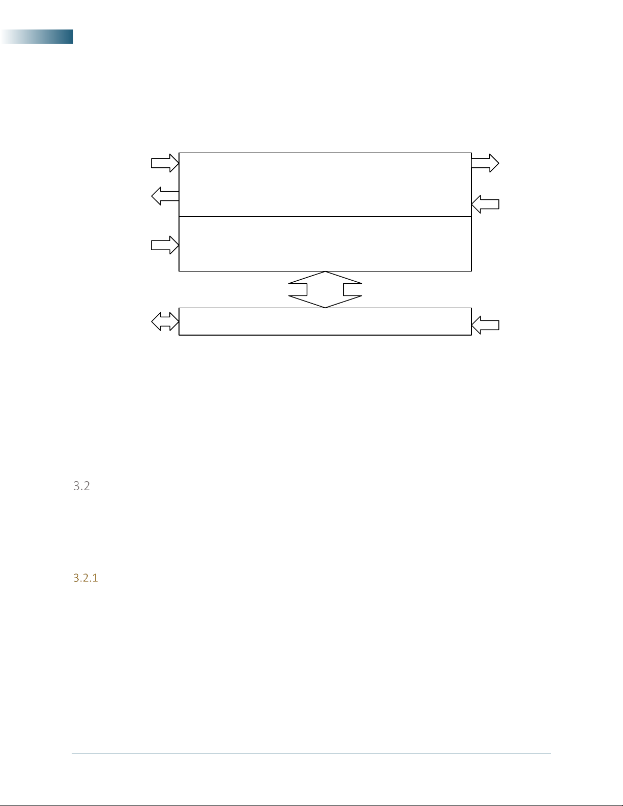
The downconverter assembly consists of 2 module parts:
•The Signal Conversion Module contains the mixers, filters, signal amplifiers, and attenuators, also
referred to as the “signal chain”. This conversion module also includes a built-in LO synthesizer.
Figure 2. Proper Removal of Latching-Style Ribbon Cable Connectors
Rev 1.1 | SC5317A & SC5318A Hardware Manual SignalCore, Inc.
10
SC5317A & SC5318A Hardware Manual
•The Power Conditioning and Digital Control Board contains the supply switcher that generates
the needs rails for the RF modules and an onboard MCU that provides both the computation
engine and interface between the user and the RF modules.
The figure below shows how the modules relate to each other.
Figure 3. Simplified Block Representation of the Downconverter Assembly Module
The downconverter has only a single conversion stage that converts the RF signal to an intermediate
frequency (IF) stage. The input range of this downconverter is from 6 GHz to 26.5 GHz, while the output
IF range is from 50 MHz to 3000 MHz. The LO signal can be selected from the internal synthesizer or an
external signal generator. The frequency accuracy and stability of the internal LO is derived from an
onboard TCXO with accuracy of better than 500 ppb. For better accuracy and stability, the synthesizer can
lock to an external reference of higher precision.
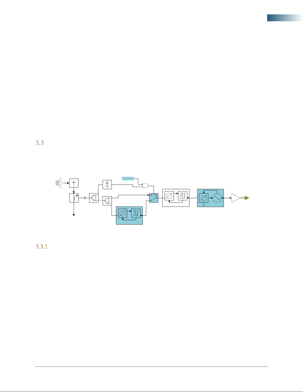
The Signal Chain
The conversion module contains the mixers, filters, amplifiers, and attenuators used to convert, purify,
and maintain the amplitude of the signal, all the way from the input of the device to its output. This
cascade of signal conversion and conditioning stages is often referred to as the signal chain, which is
shown on the system block drawing of the next figure.
The RF Input
All RF connectors are SMA types rated to 26.5 GHz of operation. The RF port is AC coupled with a 0.1
broadband capacitor as indicated in the next figure. The input frequency range at this port is less than 6
GHz to greater than 26.5 GHz. The upper limit to which the device tunes to above 26.5 GHz varies slightly
from unit to unit depending on the limits of the oscillator circuitry. The usability of the upper out-of-
bounds region depends on the roll-off response of the mixer.
Signal Conversion
Synthesized Local Oscillator
Supply Conditioning and Digital Control/Interface
RF Input
LO/Ref
Front
Digital IO Supply
IF Output
LO Rear
RF Bypass
Out

©2018 Rev 1.1
11
Functional Description
Figure 4. Block diagram of the downconverter assembly
The Input Path Switch
Immediately following the capacitor is a RF switch to selectively direct the RF signal down two paths:
1. The default is the conversion path where the RF signal is converted to an IF.
2. The alternative path is directly to the RF output port, bypassing all means of frequency
conversion. The upper frequency limit of this path is about 7 GHz, although path loss calibration is
only up to 6 GHz.
When the conversion path is bypassed, the conversion path and the internal LO are disabled by powering
down.
The RF Path
The first device in the RF conversion path is a step attenuator with 1 dB step resolution. This attenuator
(RF_ATTEN) is used to control the signal level at the mixer or at the RF preamplifier. If the RF level at the
input of these devices is relatively large with respect to their input compression points, the signal would
experience greater nonlinear effects, distorting its waveform, and producing large spurious 3rd
intermodulation distortion effects.
Following RF_ATTEN is a switchable RF amplifier that can be switched into the signal path to improve the
device sensitivity, effectively lowering the device noise figure. In other words, the effective input noise
level of the device is lowered when this amplifier is enabled. When signals with levels lower than -30 dBm
are expected, turning on this amplifier is recommended to improve the signal-to-noise dynamic range
(DRSNR). The typical maximum gain of the downconverter without the amplifier enabled is +20 dB, and
when the amplifier is enabled, its additional +20 dB will boost the typical maximum gain to +45 dB.
There are no band selective filters in the RF path so in open environments the device is unable to
differentiate a RF signal from its image. A band select filter at the RF input port is recommended to
properly filter out the signal of interest before down conversion.
R
I
L
2
RF_PREAMP
LNA
6-26.5 GHz
LPF
3.5 GHz
LPF
10 M - 3.5 GHz
RF_ATTEN
30 GHz DSA
0 to 31 dB
1 dB step
IF_ATTEN
6 GHz DSA
0 to 31.75 dB
.25 dB step
Front LO /
Reference
DC coupled
<13.5 GHz
>13.5 GHz
10 MHz
Reference In
Internal LO
Synthesizer
GHz
1 Hz step
LO Out
RF Bypass
Output
Rear LO
DC coupled
IF Out
~DC to 3.5 GHz
RF In
6 to 26.5 GHz
50
50IF Amp
IF Amp
IF Amp
RF
Linear
Amp
LO
Buffer
Amp
LPF
50 MHz
HPF
6 GHz
~DC GHz Bypass
User
controlled
component

Rev 1.1 | SC5317A & SC5318A Hardware Manual SignalCore, Inc.
12
SC5317A & SC5318A Hardware Manual
The First Mixer and IF Path
The mixer (RF mixer) of the downconverter is very critical as it sets the dynamic ranges of the device,
both the signal-to-noise and third order IMD (DRIMD) dynamic ranges. The DRSNR and DRIMD are directly
related to the mixer input compression point (IP1dB) and input third-order intercept point (IIP3). The IIP3
of the mixer is typically better than +18 dBm, and its P1dB is better than 5 dBm. In applications that
require better signal linearity, it is recommended that the level at the mixer input is kept at -20 dBm or
less. Typically, the IMD is better than -75 dBc for two -20 dBm tones at the mixer. Increasing the level at
the mixer improves SNR of the IF output signal at the expense of higher nonlinear byproducts.
Another important characteristic of the mixer is the LO-IF isolation and LO-RF isolation. The higher the
isolation, the lower the leakage LO signal is at the RF and IF ports. The RF mixer is driven with a ~+17 dBm
LO signal and the LO-IF isolation is about 45 dB, resulting in a -28 dBm LO leakage in the IF path. The low-
pass IF filters suppress this leakage to levels well below -60 dBm. The LO-RF isolation is also about 45 dB
so the LO leakage at the RF port of the mixer is on the order of -28 dBm. The high reverse isolation of the
RF linear power amplifier suppresses this LO leakage to < 60 dBm. When the low noise pre-amplifier is
enabled, it will provide another 30 dB of reverse isolation, lowering the LO leakage at the RF input port to
< 90 dBm.
The frequency relationship between the three ports of the mixer is given as:
From the above equation, the IF output spectrum is inverted with respect to the RF in the first
relationship, whereas in the second it is noninverted. When the LO > RF, the IF signal is inverted and it is
not inverted when LO < RF.
Signal Chain Configurations
Recommended signal chain configurations are provided below for various application scenarios. These
are strictly recommendations, they are not an indicative of the downconverter function limitations; users
will need to adapt the device to their applications at hand.
Signals Bypassing the Conversion Stage
For frequency less than 6 GHz, the RF input signal can be directed to the RF output port, bypassing the
conversion process. This RF output signal may be used by another downconverter to bring it down to
baseband IF, for example, the SC5308A 6 GHz downconverter mates well with this device to form an
integrated converter with continuous frequency coverage from 100kHz to 26.5 GHz.
Dynamic Range Setting
There are 2 digital step attenuators to control the conversion gain of the downconverter, the RF_ATTEN
in the RF stage and IF_ATTEN in the IF stage. Both attenuators have 30 dB of settable range, however the
IF attenuator has fine resolution of 0.25 dB while the RF attenuator has resolution of 1 dB.
To set the downconverter for better sensitivity or better SNR, the gain should be shifted to the RF input
path of the device, before the mixer. The RF pre-amplifier should be enabled if necessary and/or RF
attenuation reduced. The IF attenuator is then used to adjust the final IF output level. The drawback is
©2018 Rev 1.1
13
Functional Description
that the signal level starts off higher as it enters the first mixer as well as subsequent components such
that the apparent linearity of the device is lower.
To set the device for better linearity, the gain should be shifted to the output IF path, after the mixer, and
reducing the gain in the RF path. The signal power level at the first mixer should be lower than -20 dB for
improved linearity. Since the input signal is low, the relative SNR will be lower. But, as the first mixer and
subsequent components experience lower power levels, the apparent linearity of the device is improved.
When the device gain is balanced well, the device could achieve SNR of better than 130 dBc/Hz while
maintaining IMD3 levels close to 75 dBc. These numbers are representative of converters used in large
box high end spectrum analyzers. When the device is optimized for best SNR, typical numbers > -150
dBc/Hz can be achieved, and when the device is optimized for sensitivity, the input spectral noise floor is
typically lower than -165 dBm/Hz. The flexible use of these attenuators and pre-amplifier allows the
downconverter to achieve better than 190 dB of measurement dynamic range.
The LO Synthesizer and External Ports
The internal LO synthesizer is a hybrid between integer-N PLL and DDS, enabling it to tune at 1 Hz step
while maintaining low phase noise. The reference signal for the generation of the LO signal comes from
an internal temperature-controlled crystal oscillator (TCXO).
Figure 5. Block diagram of the local oscillator
The Reference Clocks
The base clock of the downconverter is a 10 MHz voltage-controlled temperature-controlled crystal
oscillator (VCTCXO) with initial accuracy of better than 500 ppb once the device has reached a stable
temperature. Its initial accuracy is set at the factory via an on-board 14-bit voltage reference DAC. This
DAC is accessible for dynamic accuracy calibration. The other reference is a 100 MHz voltage-controlled
crystal oscillator (VCXO), which is phase locked to the base reference whenever an external reference
source is not used.
When an external reference is selected as the base clock by enabling the device to phase lock to it, the
effect only occurs when the presence of this reference is detected. In other words, although the device is
programmed to lock externally it will not attempt to do so until the reference signal is detected at the
input reference port. Notice, both the reference clocks (TCXO and VCXO) will attempt to lock to the
external source. Having the VCXO lock directly to the external source has the advantage of utilizing the
close-in phase noise of the source; it is best to assume that the external source is superior to the internal
base. Although the internal VCTCXO is not used when an external reference is selected, it is important to
100M PLL
REF DETECT
ENABLE
LO
TCXO PLL
LO/
Ref In
To
Mixer
To
Mixer

Rev 1.1 | SC5317A & SC5318A Hardware Manual SignalCore, Inc.
14
SC5317A & SC5318A Hardware Manual
have it remain powered on to maintain its temperature stability. Like the VCXO, it is also phase locked to
the external source.
LO Ports
There are 2 selectable LO ports, one located in the front of the device and the other on the opposite end
(rear). The port in the front is shared between the external LO and reference clock. A coupler exists
internally to direct the 10 MHz reference signal to the internal LO circuitry for phase locking. The
frequency range of the LO is between 6 GHz and 18 GHz and its signal can be doubled with the internal
doubler to 26.5 GHz. The input frequency range of the doubler is from 13.5 GHz to 27 GHz.
The Interface Module
The following figure shows the power and control interface block for the SC5318A. All supply rails are
produced on board; their voltages are regulated and actively filtered to keep noise to a minimum. Thus,
these downconverters are tolerant to “dirty” external power supplies.
Figure 6. Block diagram of the power and interface module
4Hardware Registers
The set of hardware registers of the downconverter may be divided into a configuration set and a query
set; the configuration registers are write-only registers to set up the states of the device, while the query
registers request the device to prepare and send back data associated with them. The registers are
identical for all communication interfaces: USB, RS232, and SPI. Data communication to all interfaces are
sent in 1 byte wide, that is, data is transferred byte-by-byte. Register data lengths vary in size, and it is
important that the correct number of bytes are sent for the corresponding register. Failure to do so may
cause communication to lock-up and the device to become unresponsive.
Configuration Registers
These are write-only registers to configure the device. The registers vary in length to reduce redundant
data and improve the communication speed, especially for SPI and RS232 interfaces. Furthermore, it is
vitally important that the length of data written to a register is exact because failure to do so will cause
the interfaces to misinterpret the incoming data, leaving the device in a stalled state. The total number of
+18V, +10V, +5V, +3.3V,
-5V, -10V
To LO & SignalChain Module
MCU
Switchers and regulators
PXI Power PXIe Interface
Ext.Power
+12V USB RS232,
SPI
PXIe-Serial
Bridge
SC5317A
SC5318A

©2018 Rev 1.1
15
Hardware Registers
bytes is the sum of the register address (1 Byte) and its corresponding data bytes. For example, to set the
RF frequency value, eight bytes must be written; the sum of the 1 register byte and 7 data bytes. See the
RF_FREQUENCY register of Table 5. The table provides a summary of the configuration registers, and each
register is explained in detail.
Table 4. Configuration Registers
Register Name
Reg Add
Serial
Range
Bit 7
Bit 6
Bit 5
Bit 4
Bit 3
Bit 2
Bit 1
Bit 0
INITIALIZE
0x01
[7:0]
Set to zeros [7:1]
Mode
SYSTEM_ACTIVE
0x02
[7:0]
Set to zeros [7:1]
Enable “active” LED
SYNTH_MODE
0x03
[7:0]
Set to zeros [7:2]
Fast-tune
Loop Gain
RF_FREQUENCY
0x10
[7:0]
Frequency Word (Hz) [7:0]
[15:8]
Frequency Word (Hz) [15:8]
[23:16]
Frequency Word (Hz) [23:16]
[31:24]
Frequency Word (Hz) [31:24]
[39:32]
Frequency Word (Hz) [39:32]
[47:40]
Frequency Word (Hz) [47:40]
[55:48]
Frequency Word (Hz) [55:48]
IF_FREQUENCY
0x11
[7:0]
Frequency Word (Hz) [7:0]
[15:8]
Frequency Word (Hz) [15:8]
[23:16]
Frequency Word (Hz) [23:16]
[31:24]
Frequency Word (Hz) [31:24]
[39:32]
Frequency Word (Hz) [39:32]
[47:40]
Frequency Word (Hz) [47:40]
[55:48]
Frequency Word (Hz) [55:48]
LO_FREQUENCY
0x12
[7:0]
Frequency Word (Hz) [7:0]
[15:8]
Frequency Word (Hz) [15:8]
[23:16]
Frequency Word (Hz) [23:16]
[31:24]
Frequency Word (Hz) [31:24]
[39:32]
Frequency Word (Hz) [39:32]
[47:40]
Frequency Word (Hz) [47:40]
[55:48]
Frequency Word (Hz) [55:48]
RF_AMP
0x13
[7:0]
RF_AMP
0x14
[7:0]
Set to zeros [7:1]
Enable
ATTENUATOR
0x15
[7:0]
Attenuator Value
[15:8]
Set to zeros [15:11]
Attenuator Number
[23:16]
Set to zeros [23:16]
SIGNAL_PATH
0x16
[7:0]
Set to zeros [7:4]
Invert
Spectrm
IF Out
Enable
Amp
Enable
Bypass
convert
STORE_DEFAULT_ STATE
0x18
[7:0]
Set all to zeros
DEVICE_STANDY
0x19
[7:0]
Set to zeros [7:1]
Enable
REFERENCE_CLOCK
0x1A
[7:0]
[7:2] set to zeros
PXI 10
enable
Lock ext
REFERENCE_DAC
0x1B
[7:0]
DAC WORD [7:0]
[15:8]
zeros [15:14]
DAC WORD [13:8]
[23:16]
Set to zeros
USER_EEPROM_ WRITE
0x1D
[7:0]
BYTE DATA [7:0]
[15:8]
ADDRESS [7:0]
[23:16]
ADDRESS [15:8]
SYNTH_SELF_CAL
0x1F
[7:0]
Set all to zeros
Register 0x02 SET_SYS_ACTIVE
This register turns on or off the active LED indicator on the front connector interface of the device. This
register should be called when the device is opened or closed in software.

Rev 1.1 | SC5317A & SC5318A Hardware Manual SignalCore, Inc.
16
SC5317A & SC5318A Hardware Manual
Bytes written
2
Bytes read
1
Bits
Type
Name
Width
Description
[0]
WO
Mode
1
0 = turns off the active LED
1 = turns on the active LED
[7:1]
WO
Unused
7
Set to zeros
[7:0]
RO
Read back byte
8
Read 1 byte back is required for PXIe and RS232
Register 0x03 SYTHN_MODE (2 Bytes)
This register configures the PLL loop gain of the local oscillator synthesizers. It also enables or disables
faster tuning of the YIG based oscillator of LO1.
Bytes written
2
Bytes read
1
Bits
Type
Name
Width
Description
[1:0]
WO
Loop Gain
2
0 = low loop gain, improves phase noise > 50 kHz
1 = normal loop gain
2 = high loop gain, improves phase noise < 50 kHz
[2]
WO
Fast Tune
1
0 = turns fast tune off, default
1 = turns fast tune on, close in phase noise may
degrade
[7:3]
WO
Unused
5
Set to zeros
[7:0]
RO
Read back byte
8
Read 1 byte back is required for PXIe and RS232
Register 0x10 RF_FREQUENCY
This register tunes the device to the input RF frequency.
Bytes written
8
Bytes read
1

©2018 Rev 1.1
17
Hardware Registers
Bits
Type
Name
Width
Description
[55:0]
W
Frequency word
56
Frequency word in milli-Hz (mHz), mHz used for
future compatibility
[7:0]
RO
Read back byte
8
Read 1 byte back is required for PXIe and RS232
Register 0x11 IF_FREQUENCY
This register sets the final IF value.
Bytes written
2
Bytes read
1
Bits
Type
Name
Width
Description
[55:0]
W
Frequency word
56
Frequency word in milli-Hz (mHz), mHz used for
future compatibility
[7:0]
R
Read back byte
8
Read 1 byte back is required for PXIe and RS232
Register 0x12 LO_FREQUENCY
This register sets the final IF value.
Bytes written
2
Bytes read
1
Bits
Type
Name
Width
Description
[55:0]
W
Frequency word
56
Frequency word in milli-Hz (mHz), mHz used for
future compatibility
[7:0]
R
Read back byte
8
Read 1 byte back is required for PXIe and RS232
Register 0x14 RF_AMP
This register enables and disables the RF amplifier.
Bytes written
2
Bytes read
1
Bits
Type
Name
Width
Description
[0]
W
Frequency word
1
0 = disables the RF amplifier

Rev 1.1 | SC5317A & SC5318A Hardware Manual SignalCore, Inc.
18
SC5317A & SC5318A Hardware Manual
Bits
Type
Name
Width
Description
1 = enables the RF amplifier
[7:1]
W
Unused
7
Set to zeros
[7:0]
R
Read back byte
8
Read 1 byte back is required for PXIe and RS232
Register 0x15 ATTENUATOR
This register sets the value of the device attenuators.
Bytes written
4
Bytes read
1
Bits
Type
Name
Width
Description
[7:0]
W
Attenuator value
8
In 0.25 dB LSB for IF, 1 dB LSB for RF
[10:8]
W
The target
attenuator
3
The attenuator number:
0 = RF Atten
1 = RF Atten
[23:11]
W
Unused
13
Set to zeros
[7:0]
R
Read back byte
8
Read 1 byte back is required for PXIe and RS232
Register 0x16 SIGNAL_PATH
This register configures how the signal chain is routed.
Bytes written
2
Bytes read
1
Bits
Type
Name
Width
Description
[0]
W
Bypass Converter
1
0 = Normal conversion path
1 = Bypasses the conversion, switches RF input
directly to RF output
[1]
W
RF Amp Enable
1
0 = Turns off RF preamplifier
1 = Turns on RF preamplifier
[2]
W
IF Out Enable
1
0 = Disables the IF output port
©2018 Rev 1.1
19
Hardware Registers
Bits
Type
Name
Width
Description
1 = Enables the IF output port
[3]
W
Invert Spectrum
1
0 = Sets the LO to invert the IF spectrum
1 = Sets the LO to not invert the IF spectrum
[7:4]
W
Not used
14
Set to zeros
[7:0]
R
Read back byte
8
Read 1 byte back is required for PXIe and RS232
Register 0x18 STORE_DEFAULT_STATE
This register will store all current settings of the device into EEPROM and will become the default startup
setting.
Bytes written
2
Bytes read
1
Bits
Type
Name
Width
Description
[7:0]
W
Unused
8
Set to zeros
[7:0]
R
Read back byte
8
Read 1 byte back is required for PXIe and RS232
Register 0x19 DEVICE_STANDBY
This register sets either the entire device or sections of the device into standby mode. Placing a section
into standby involves powering down its circuitry. This conserves power and eliminates unwanted LO
signals when they are not used.
Bytes written
2
Bytes read
1
Bits
Type
Name
Width
Description
[0]
W
State
1
0 = Powers down analog section
1 = Enables and powers on analog section
[7:1]
W
Unused
4
Set to zeros
[7:0]
R
Read back byte
8
Read 1 byte back is required for PXIe and RS232
Other manuals for SC5317A
1
This manual suits for next models
1
Table of contents
Other SIGNALCORE Media Converter manuals


Popular Media Converter manuals by other brands


Siko
Siko ProTool SGH50 quick start guide

Transition Networks
Transition Networks CFMFF1314-280 user guide

DesignTech
DesignTech MIPC-1A quick start guide

SecurityMan
SecurityMan SM-401 instruction manual
Pixel Magic
Pixel Magic Crystalio II owner's guide

Baumer
Baumer HUBNER BERLIN HOG 75 D1C Mounting and operating instructions


