SIGNALCORE SC5305A Owner's manual

© 2012-2015 SignalCore, Inc.
support@signalcore.com
SC5305A
1 MHz to 3.9 GHz RF Downconverter
for PXI Express
Operating & Programming Manual

SC5305A Operating & Programming Manual Rev 2.0.0 i
CO N T E N T S
Important Information 1
Warranty 1
Copyright & Trademarks 2
International Materials Declarations 2
CE European Union EMC & Safety Compliance Declaration 2
Recycling Information 3
Warnings Regarding Use of SignalCore Products 3
Getting Started 4
Unpacking 4
Verifying the Contents of your Shipment 4
Setting Up and Configuring the SC5305A 4
Signal Connections 6
Indicator LEDs 6
SC5305A - Theory of Operation 7
Overview 7
Signal Path Description 8
Local Oscillator Description 11
Frequency Tuning Modes 12
Setting the SC5305A to Achieve Best Dynamic Range 13
Operating the SC5305A Outside Normal Range 14
SC5305A Programming Interface 15
Device Drivers 15
Using the Application Programming Interface (API) 15
Setting the SC5305A - Writing To Configuration Registers 16
Configuration Registers 16
Tuning the RF Frequency 16
Changing the Attenuator Settings 17
Enabling and Disabling the RF Preamplifier 17
Changing the RF Synthesizer Mode 17

SC5305A Operating & Programming Manual Rev 2.0.0 ii
Selecting the IF Filter Path 17
Setting the Reference Clock Behavior 17
Adjusting the Reference Clock Accuracy 18
Setting Spectral Inversion in the IF 18
Storing Data into the User EEPROM Space 18
Setting the Phase of the IF Signal 18
Querying the SC5305A - Writing To Request Registers 19
Reading the Device Status 19
Reading the Device Temperature 20
Reading the Calibration EEPROM 21
Reading the User EEPROM 21
Working With Calibration Data 22
EEPROM Data Content 23
Frequency Correction 25
Gain Correction 25
IF Response Correction 27
Software API Library Functions 29
Constants Definitions 30
Type Definitions 31
Function Definitions and Usage 32
Calibration & Maintenance 47
Appendix A - Specifications 49

SC5305A Operating & Programming Manual Rev 2.1.0 1
The warranty terms and conditions for all SignalCore products are also provided on our corporate
website. Please visit http://www.signalcore.com/ for more information.
IM P O R T A N T IN F O R M A T I O N
Warranty
This product is warranted against defects in materials and workmanship for a period of one year from
the date of shipment. SignalCore will, at its option, repair or replace equipment that proves to be
defective during the warranty period. This warranty includes parts and labor.
Before any equipment will be accepted for warranty repair or replacement, a Return Material
Authorization (RMA) number must be obtained from a SignalCore customer service representative and
clearly marked on the outside of the return package. SignalCore will pay all shipping costs relating to
warranty repair or replacement.
SignalCore strives to make the information in this document as accurate as possible. The document has
been carefully reviewed for technical and typographic accuracy. In the event that technical or
typographical errors exist, SignalCore reserves the right to make changes to subsequent editions of this
document without prior notice to possessors of this edition. Please contact SignalCore if errors are
suspected. In no event shall SignalCore be liable for any damages arising out of or related to this
document or the information contained in it.
EXCEPT AS SPECIFIED HEREIN, SIGNALCORE, INCORPORATED MAKES NO WARRANTIES, EXPRESS OR
IMPLIED, AND SPECIFICALLY DISCLAIMS ANY WARRANTY OF MERCHANTABILITY OR FITNESS FOR A
PARTICULAR PURPOSE. CUSTOMER’S RIGHT TO RECOVER DAMAGES CAUSED BY FAULT OR
NEGLIGENCE ON THE PART OF SIGNALCORE, INCORPORATED SHALL BE LIMITED TO THE AMOUNT
THERETOFORE PAID BY THE CUSTOMER. SIGNALCORE, INCORPORATED WILL NOT BE LIABLE FOR
DAMAGES RESULTING FROM LOSS OF DATA, PROFITS, USE OF PRODUCTS, OR INCIDENTAL OR
CONSEQUENTIAL DAMAGES, EVEN IF ADVISED OF THE POSSIBILITY THEREOF. This limitation of the
liability of SignalCore, Incorporated will apply regardless of the form of action, whether in contract or
tort, including negligence. Any action against SignalCore, Incorporated must be brought within one year
after the cause of action accrues. SignalCore, Incorporated shall not be liable for any delay in
performance due to causes beyond its reasonable control. The warranty provided herein does not cover
damages, defects, malfunctions, or service failures caused by owner’s failure to follow SignalCore,
Incorporated’s installation, operation, or maintenance instructions; owner’s modification of the product;
owner’s abuse, misuse, or negligent acts; and power failure or surges, fire, flood, accident, actions of
third parties, or other events outside reasonable control.

SC5305A Operating & Programming Manual Rev 2.1.0 2
Copyright & Trademarks
Under the copyright laws, this publication may not be reproduced or transmitted in any form, electronic
or mechanical, including photocopying, recording, storing in an information retrieval system, or
translating, in whole or in part, without the prior written consent of SignalCore, Incorporated.
SignalCore, Incorporated respects the intellectual property rights of others, and we ask those who use
our products to do the same. Our products are protected by copyright and other intellectual property
laws. Use of SignalCore products is restricted to applications that do not infringe on the intellectual
property rights of others.
“SignalCore”, “signalcore.com”, and the phrase “preserving signal integrity” are registered trademarks
of SignalCore, Incorporated. Other product and company names mentioned herein are trademarks or
trade names of their respective companies.
International Materials Declarations
SignalCore, Incorporated uses a fully RoHS (Restriction of Hazardous Substances) compliant
manufacturing process for our products. Therefore, SignalCore hereby declares that its products do not
contain restricted materials as defined by European Union Directive 2011/65/EU (EU RoHS) in any
amounts higher than limits stated in the directive. This statement is based on the assumption of reliable
information and data provided by our component suppliers and may not have been independently
verified through other means. For products sold into China, we also comply with the “Administrative
Measure on the Control of Pollution Caused by Electronic Information Products” (China RoHS). In the
current stage of this legislation, the content of six hazardous materials must be explicitly declared. Each
of those materials, and the categorical amount present in our products, are shown below:
組成名稱
Model Name
鉛
Lead
(Pb)
汞
Mercury (Hg)
镉
Cadmium
(Cd)
六价铬
Hexavalent
Chromium
(Cr(VI))
多溴联苯
Polybrominated
biphenyls
(PBB)
多溴二苯醚
Polybrominated
diphenyl ethers
(PBDE)
SC5305A
A indicates that the hazardous substance contained in all of the homogeneous materials for this
product is below the limit requirement in SJ/T11363-2006. An X indicates that the particular hazardous
substance contained in at least one of the homogeneous materials used for this product is above the
limit requirement in SJ/T11363-2006.
CE European Union EMC & Safety Compliance Declaration
The European Conformity (CE) marking is affixed to products with input of 50 - 1,000 VAC or 75 - 1,500
VDC and/or for products which may cause or be affected by electromagnetic disturbance. The CE
marking symbolizes conformity of the product with the applicable requirements. CE compliance is a
manufacturer’s self-declaration allowing products to circulate freely within the European Union (EU).
SignalCore products meet the essential requirements of Directives 2014/30/EU (EMC) and 2014/35/EU

SC5305A Operating & Programming Manual Rev 2.1.0 3
(product safety), and comply with the relevant standards. Standards for Measurement, Control and
Laboratory Equipment include EN 61326-1:2013 and EN 55011:2009 for EMC, and EN 61010-1 for
product safety.
Recycling Information
All products sold by SignalCore eventually reach the end of their useful life. SignalCore complies with EU
Directive 2012/19/EU regarding Waste Electrical and Electronic Equipment (WEEE).
Warnings Regarding Use of SignalCore Products
(1)
PRODUCTS FOR SALE BY SIGNALCORE, INCORPORATED ARE NOT DESIGNED WITH COMPONENTS NOR TESTED FOR A LEVEL OF
RELIABILITY SUITABLE FOR USE IN OR IN CONNECTION WITH SURGICAL IMPLANTS OR AS CRITICAL COMPONENTS IN ANY LIFE SUPPORT
SYSTEMS WHOSE FAILURE TO PERFORM CAN REASONABLY BE EXPECTED TO CAUSE SIGNIFICANT INJURY TO A HUMAN.
(2)
IN ANY APPLICATION, INCLUDING THE ABOVE, RELIABILITY OF OPERATION OF THE SOFTWARE PRODUCTS CAN BE IMPAIRED BY ADVERSE
FACTORS, INCLUDING BUT NOT LIMITED TO FLUCTUATIONS IN ELECTRICAL POWER SUPPLY, COMPUTER HARDWARE MALFUNCTIONS,
COMPUTER OPERATING SYSTEM SOFTWARE FITNESS, FITNESS OF COMPILERS AND DEVELOPMENT SOFTWARE USED TO DEVELOP AN
APPLICATION, INSTALLATION ERRORS, SOFTWARE AND HARDWARE COMPATIBILITY PROBLEMS, MALFUNCTIONS OR FAILURES OF
ELECTRONIC MONITORING OR CONTROL DEVICES, TRANSIENT FAILURES OF ELECTRONIC SYSTEMS (HARDWARE AND/OR SOFTWARE),
UNANTICIPATED USES OR MISUSES, OR ERRORS ON THE PART OF THE USER OR APPLICATIONS DESIGNER (ADVERSE FACTORS SUCH AS
THESE ARE HEREAFTER COLLECTIVELY TERMED “SYSTEM FAILURES”). ANY APPLICATION WHERE A SYSTEM FAILURE WOULD CREATE A
RISK OF HARM TO PROPERTY OR PERSONS (INCLUDING THE RISK OF BODILY INJURY AND DEATH) SHOULD NOT BE SOLELY RELIANT
UPON ANY ONE COMPONENT DUE TO THE RISK OF SYSTEM FAILURE. TO AVOID DAMAGE, INJURY, OR DEATH, THE USER OR
APPLICATION DESIGNER MUST TAKE REASONABLY PRUDENT STEPS TO PROTECT AGAINST SYSTEM FAILURES, INCLUDING BUT NOT
LIMITED TO BACK-UP OR SHUT DOWN MECHANISMS. BECAUSE EACH END-USER SYSTEM IS CUSTOMIZED AND DIFFERS FROM
SIGNALCORE' TESTING PLATFORMS, AND BECAUSE A USER OR APPLICATION DESIGNER MAY USE SIGNALCORE PRODUCTS IN
COMBINATION WITH OTHER PRODUCTS IN A MANNER NOT EVALUATED OR CONTEMPLATED BY SIGNALCORE, THE USER OR
APPLICATION DESIGNER IS ULTIMATELY RESPONSIBLE FOR VERIFYING AND VALIDATING THE SUITABILITY OF SIGNALCORE PRODUCTS
WHENEVER SIGNALCORE PRODUCTS ARE INCORPORATED IN A SYSTEM OR APPLICATION, INCLUDING, WITHOUT LIMITATION, THE
APPROPRIATE DESIGN, PROCESS AND SAFETY LEVEL OF SUCH SYSTEM OR APPLICATION.

SC5305A Operating & Programming Manual Rev 2.1.0 4
Ground yourself using a grounding strap or by touching a grounded metal object.
Touch the antistatic bag to a grounded metal object before removing the hardware
from its packaging.
Never touch exposed signal pins. Due to the inherent performance degradation
caused by ESD protection circuits in the RF path, the device has minimal ESD
protection against direct injection of ESD into the RF signal pins.
When not in use, store all SignalCore products in their original antistatic bags.
GE T T I N G ST A R T E D
Unpacking
All SignalCore products ship in antistatic packaging (bags) to prevent damage from electrostatic
discharge (ESD). Under certain conditions, an ESD event can instantly and permanently damage several
of the components found in SignalCore products. Therefore, to avoid damage when handling any
SignalCore hardware, you must take the following precautions:
Remove the product from its packaging and inspect it for loose components or any signs of damage.
Notify SignalCore immediately if the product appears damaged in any way.
Verifying the Contents of your Shipment
Verify that your SC5305A kit contains the following items:
Quantity
Item
1
SC5305A RF Downconverter for PXI Express
1
Software Installation USB Flash Drive (may be combined with other products onto a single drive)
Setting Up and Configuring the SC5305A
The SC5305A is a designed for use in a PXI Express (PXIe) or PXIe hybrid chassis. Chassis manufacturers
must provide at least the minimum required per-slot power dissipation cooling capability to be
compliant with the PXIe specifications. The SC5305A is designed to be sufficiently cooled in either all-
PXIe chassis or PXIe hybrid chassis (chassis with a mix of PXI Express slots and traditional PXI slots).
However, certain environmental factors may degrade performance. Inadequate cooling can cause the
temperature inside the RF housing to rise above the maximum for this product, leading to improper
performance and potentially reducing product lifespan or causing complete product failure. Maintain
adequate air space around the chassis at all times, and keep the chassis fan filters clean and
unobstructed.
Refer to your chassis manufacturer’s user manual for proper setup and maintenance of your
PXIe or PXIe hybrid chassis. The SC5305A on-board temperature sensor should indicate a rise
of no more than 20 °C above ambient temperature under normal operating conditions.
!
!

SC5305A Operating & Programming Manual Rev 2.1.0 5
The SC5305A is a PXIe RF downconverter with all user I/O located on the front face of the module as
shown in Figure 1. Each I/O location is discussed in further detail below.
Figure 1. PXI Express chassis view of the SC5305A. Module is shown installed in slot 2.
All signal connections (ports) on the SC5305A are SMA-type, with the exception of the PXI backplane
clock connection (MCX connection). Exercise caution when fastening cables to the signal connections.
Over-tightening any connection can cause permanent damage to the device.
The condition of your system‘s signal connections can significantly affect measurement
accuracy and repeatability. Improperly mated connections or dirty, damaged or worn
connectors can degrade measurement performance. Clean out any loose, dry debris from
connectors with clean, low-pressure air (available in spray cans from office supply stores).
If deeper cleaning is necessary, use lint-free swabs and isopropyl alcohol to gently clean
inside the connector barrel and the external threads. Do not mate connectors until the
alcohol has completely evaporated. Excess liquid alcohol trapped inside the connector may
take several days to fully evaporate and may degrade measurement performance until fully
evaporated.
Tighten all SMA connections to 5 in-lb max (56 N-cm max)
!
!

SC5305A Operating & Programming Manual Rev 2.1.0 6
Signal Connections
RF IN This port accepts input signals from 1 MHz to 3.9 GHz to the downconverter. The nominal
input impedance is 50 Ω. Maximum input power is +27 dBm.
IF OUT This port outputs the 70 MHz IF signal from the downconverter. The nominal output
impedance is 50 Ω.
REF IN This port accepts an external 10 MHz reference signal, allowing an external source to
synchronize the internal reference clock. This port is AC-coupled with a nominal input
impedance of 50 Ω. Maximum input power is +13 dBm.
REF OUT This port outputs the internal 10 MHz or 100 MHz reference clock. If the internal reference
clock is synchronized to an external reference clock through the 10 MHz “ref in”port, this
output port will also be synchronized. This port is AC- coupled with a nominal output
impedance of 50 Ω.
PXI CLK10 This port outputs the 10 MHz chassis reference signal from the chassis backplane, allowing it
to synchronize the internal reference clock. An MCX male to SMA male cable is required (but
not supplied) to connect this port to the “ref in”port in order to use this reference for
synchronization. This port may be enabled or disabled through a software switch to
minimize possible clock noise when not in use. This port has a nominal output impedance of
50 Ω and drives 0 dBm into a 50 Ω load.
Indicator LEDs
The SC5305A provides visual indication of important modes. There are two LED indicators on the device.
Their behavior under different operating conditions is shown in Table 1.
Table 1. LED indicator states.
LED
Color
Definition
STATUS
Green
“Power good” and all oscillators phase-locked
STATUS
Red
One or more oscillators off lock
STATUS
Off
Power fault
ACTIVE
Green/Off
Device is open (green) /closed (off) , this indicator is also
user programmable (see register map)
ACTIVE
Orange
User initiated standby mode

SC5305A Operating & Programming Manual Rev 2.1.0 7
S C 5 3 0 5 A TH E O R Y O F OP E R A T I O N
Overview
The SC5305A operates on the principle of heterodyning, a process whereby an incoming RF signal is
mixed with specific oscillator frequencies in stages, producing both sum and difference frequency
products. At each stage the summed frequency product (or image) is removed through low-pass
filtering, allowing the difference frequency product to continue through the signal path. Repeating this
process several times using carefully selected local oscillators (LOs) and well-designed band-pass
filtering, the original signal is translated or “downconverted” in frequency low enough for inexpensive
digitizers to acquire the signal with reasonable bandwidth. The resultant output signal of a heterodyne
downconverter is known as the intermediate frequency (IF). Using a tunable LO as the first mixing
oscillator allows the downconverter to translate a broad range of frequencies to a common IF output.
When combined, a tunable LO and extraction of the lower mixed frequency product creates an
important and useful variant of the heterodyne process known as superheterodyning.
The SC5305A is a three-stage superheterodyne downconverter that delivers superior image rejection
over single stage conversion and offers both high signal-to-noise dynamic range and high spurious-free
dynamic range. The RF input ranges from 1 MHz to 3.9 GHz, and the IF output is fixed at 70 MHz. When
the input frequency is lower than the intermediate frequency, the device technically behaves as an
upconverter. The SC5305A up-converts when the input frequency ranges from 1 MHz to 70 MHz. The
converted spectrum polarity may be inverted or non-inverted by programming the device accordingly.
Fundamentally, each conversion stage consists of a frequency mixer that mixes two input signals and
producing a wanted third. The wanted third component is selected, via a frequency filter, among other
signals generated in the mixing process. The three primary components of the signals in each conversion
mixer are commonly known as the local oscillator (LO), radio frequency (RF), and the intermediate
frequency (IF) as shown in Figure 2.
Figure 2. Frequency conversion stage using a mixer.
Where R represents the RF component, L represents the LO component, and I represents the IF
component. The LO is resident in the downconverter and is either frequency tunable or fixed in
frequency depending on the stage.
The first IF stage is an upconversion stage - all input signals are converted to an IF higher than the
highest input frequency specified. The second and third stages successively convert this high first IF
down to the final IF of 70 MHz. Having a high first IF allows the downconverter to achieve very high
image rejection ability. This image-free architecture achieves high image rejection without the need for
sharp cut-off pre-select band-pass filters. Having high image rejection makes the SC5305A suitable for
L
RI
RF
LO
IF

SC5305A Operating & Programming Manual Rev 2.1.0 8
applications such as spectral monitoring, broadband spectral analysis, and others where the spectral
environment cannot be controlled.
The SC5305A exhibits very low phase noise of -107 dBc/Hz at 10 kHz offset on a 1 GHz RF carrier with a
typical noise floor of -150 dBm/Hz. The noise floor can be further reduced below -165 dBm/Hz by
enabling the internal preamplifier. With gain control between -60 dB to +50 dB, a measurement signal-
to-noise dynamic range greater than 180 dB is achievable. Using high reverse isolation devices and sharp
cutoff filters, LO leakages and other spurious contents at the input connectors are well below -120 dBm.
Inter-stage LO leakages are also kept very low through sophisticated circuit and shielding design to
ensure that spurious in-band signals remain less than -80 dBc. The excellent spurious free dynamic range
is achieved using low noise linear amplifiers, low loss mixers, and high performance solid state
attenuators. State-of-the-art solid state attenuators have improved linearity over earlier designs. Their
attenuation level changes settle under a microsecond, and for applications that involve frequent range
changing, they offer a vastly superior lifetime over mechanical attenuators.
The real-time bandwidth is shaped primarily by the final 70 MHz IF surface acoustic wave (SAW) filter.
The final IF filter has two programmatically selectable paths, switching either between two filter paths
with different bandwidths or between one filter and one bypass (no filter) path. Filters in the first and
second IF stages are not as selective as the final IF filter but they ensure good isolation between local
oscillators (LO). Keeping each LO isolated helps to suppress unwanted spurious signals.
Frequency accuracy is provided by an onboard 10 MHz temperature compensated crystal oscillator
(TCXO) which can be phase-locked to an external reference source if required, and it is recommended to
do so in applications that may require a more stable and accurate base reference.
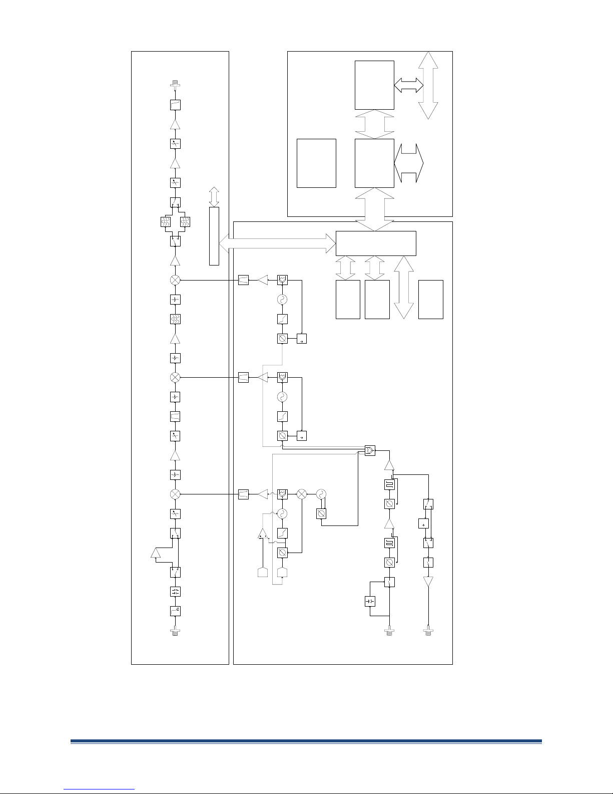
Signal Path Description
Figure 3 depicts an overall block diagram of the SC5305A. Starting from the upper left, the RF input of
the SC5305A is AC coupled, followed by an elliptic low-pass filter which has a sharp cut-off frequency
slope to ensure the images and unwanted frequencies are well suppressed. Next, a bypass switch
enables or disables the internal preamplifier in the path of the RF signal, directly after the input filter.
The advantage of placing the amplifier before the attenuators is to increase the downconverter
sensitivity when the preamplifier is selected. This switch is programmatically controlled and can be
toggled as required, enabling the preamplifier to boost input signals of very small amplitude. Due to
losses in the attenuators, the noise figure of the system is proportional to their accumulated losses if the
attenuators were placed before the amplifier. The trade-off for better sensitivity is the lack of
attenuation adjustment for larger signals when the amplifier is enabled. The user will need to provide
good judgment when enabling the preamplifier.
SC5305A Operating & Programming Manual Rev 2.1.0 9
Figure 3. Block diagram of the SC5305A.
R
I
LR
I
LR
I
L
N.M
N
R
I
L
10 MHZ
TCXO 100 MHZ
VCXO
Ref.
Detector
4000 MHz
PLL 605/745 MHz
PLL
4675MHz to
8575MHz PLL
YIG Driver
Fine Tune
DDS
Coarse Tune
PLL
DDS
DAC
RF
Filter
RF
PreAmp
RF Atten
0-30 dB 4675 MHz
Filter
IF1_Atten
0-30 dB
IF3 Atten1
0-30 dB IF3 Atten2
0-30 dB
675 MHz
Filter
IF3 FL 0
ESD
RF In
1 MHz –
3900 MHz
IF Out
70 MHz
Ref. In
10 MHz
Ref. Out
10/100 MHz
3.9 GHz Three Stage Downconverter
Nom Input level -20 dBm
Max Input level 27 dBm Nom output level 0 dBm
Max out level 20 dBm
IF3 FL 1
10
Module B
Module A
MCU
Power
Regulation
Digital Interface
Temp
Sensor
Calibration
EEPROM
PLL,
Attenuator,
ADC, DAC,
other devices
SPI, RS-232, USB
PCIe Bridge
PXIe
Switchers
Linear Reg.
Module C
Digital Interface Attenuators, Switches

SC5305A Operating & Programming Manual Rev 2.1.0 10
The RF attenuator, with a 0 to 30 dB attenuation range and attenuation steps of 1 dB, is located
between the preamplifier and the first mixer. The RF attenuator is used to set the signal amplitude to a
user-defined level at the mixer when the RF input level is higher than that level. This attenuator is
adjusted to obtain the required distortion levels. Lowering the RF level with the attenuator at the mixer
operates the device in a more linear region. However suppressing the RF level too low before the mixer
reduces the signal-to-noise ratio, so the user must set this level to compromise between noise and
linearity. The RF signal is mixed with the first local oscillator, LO1, and the difference component is
selected as the wanted intermediate frequency (IF).
The first IF stage after the RF mixer, referred to as IF1 in the programming section, is heavily filtered and
carefully amplified to maintain the best compromise between signal dynamic range and linearity. The
filters provide isolation between the first and second stage mixers to reduce in-band inter-modulation
spurious signals from the mixing of high order harmonics of the IF and LO frequencies. The filters in this
stage also suppress the mixer LO leakage. If not filtered, LO leakages can potentially cause saturation in
the preceding stages of the signal path and degrade the linearity performance of the device. There is an
adjustable attenuator following the output of the first mixer, which is used to suppress leakages from
LO1 that appear in-band when the downconverter is tuned to frequencies less than the bandwidth of
the device. For example, if the bandwidth of the system is 20 MHz, LO1 leakage will appear in-band if
the frequency is tuned below 20 MHz. Technically, LO leakages should not appear in-band until the
device is tuned below 10 MHz, but the non-ideality of the filter allows sufficient leakage at higher
frequencies. Setting this attenuator will attenuate both the IF1 signal and the LO1 leakage, making the
device respond more linearly. As always, the compromise is that the SNR will degrade. The LO1 leakage
signal will appear as DC when the IF is digitized and converted to baseband. By design, setting the IF
frequency at 4675 MHz allows sufficient frequency separation from the highest RF frequency so that the
IF1 filter, despite its non ideal roll-off response, can suppress the RF signal by more than -100 dB.
The first IF is then down-converted to the second IF of 675 MHz by mixing with the second LO (LO2).
Similarly, as with the first IF section, the second IF (IF2) section is also well filtered and amplified.
Keeping isolation between the second and third mixers is important to ensure spurious signals
generated within the device are kept significantly low when compared to the primary signal of interest.
Finally, the second IF is converted to the third and final IF by mixing with the third LO (LO3). Located in
this stage are the primary band-pass filters that define the bandwidth of the device. The final IF filters
are selectable between two filters of different bandwidths centered at 70 MHz. The standard
bandwidths for these filters are 5 MHz, 10 MHz, 20 MHz, and 40 MHz. These surface acoustic wave
(SAW) filters provide excellent filter response. The user may choose to use one of these two filter paths
as a bypass, that is, no band-pass filter in the path. One reason for bypassing the final IF filter is to
improve the group delay through the device; with the filters enabled the delay is approximately 1 s.
Bypassing the filter reduces the delay to about 100 ns, which may be preferred in some applications.
Following the band-pass filter are the IF attenuators, IF3_Atten1 and IF3_Atten2. These IF attenuators
control the IF gain of the device and set the desired output IF level at the IF output port. The
recommended output level is 0 dBm. However, the level may be set to other values that suit the
particular application. Finally, a low pass filter suppresses the harmonics of the IF signal. It is important
that the IF harmonics are kept as low as possible because they appear in-band as higher order images

SC5305A Operating & Programming Manual Rev 2.1.0 11
when digitized. The harmonics are typically below 90 dBc at the IF. In applications where this may not be
acceptable, external analog filtering is recommended.
Local Oscillator Description
The signal path circuit is separate from the local oscillator generation circuits to maximize isolation
between the RF/IF signals and the local oscillators, except for the LO injection paths into the mixers.
Although the both circuits reside within the same module, well-designed shielding and circuit layouts
ensures leakages between them are kept to a minimum.
The first local oscillator, LO1, is an agile, tunable phase-lock synthesizer. The synthesizer tunes from
4675 MHz to 8575 MHz, a tuning range of 3900 MHz. The minimum step size is 1 Hz, and is
accomplished through a multiple phase-locked loop and DDS hybrid architecture. The use of a hybrid
tuning architecture is important for improved phase noise and improved close-in phase spurious
responses. Operating LO1 at such high frequencies internally to obtain a 1 MHz to 3.9 GHz RF range
requires that the phase noise at these frequencies is sufficiently low so that the converted RF signal
phase noise is not degraded significantly. For example, to downconvert a 100 MHz RF signal, LO1 is
tuned to 4775 MHz, which is about 48 times higher in frequency than the input frequency. To further
ensure phase noise remains low farther away from the carrier, especially at 100 kHz and 1 MHz offsets,
a YIG oscillator is used. It important to realize that having a phase noise “plateau” out to several tens of
MHz, which is a very common phenomenon with VCO-based synthesizers, is not acceptable for many
applications.
Another reason for a hybrid tuning architecture is to reduce the phase spurs associated with phase-
locked loops. A simple fractional PLL may provide resolution to 1 Hz, but it cannot provide 1 Hz
frequency tuning steps with low fractional phase spurs. By using two DDS circuits to provide the 1 Hz
tuning steps and mathematically ensuring that DDS-generated spurs are suppressed within the
architecture, LO1 is made to fine tune to exact frequencies, that is, the frequency synthesized is an exact
integer multiple or division of the reference signal.
The second local oscillator, LO2, is fixed at 4.0 GHz, synthesized using an integer PLL and a fixed narrow
tune VCO with very low phase noise. The typical raw phase noise of the second stage oscillator is less
than -150 dBc/Hz @ 1 MHz offset. LO2 phase noise contribution to the overall phase noise of the device
is less than 1 dB. LO1 dominates the phase noise of the device.
The third local oscillator, LO3, is synthesized using a fractional PLL and has phase noise lower than both
LO1 and LO2, and is switchable between two frequencies: 605 MHz and 745 MHz, the later frequency
being the default. Both of these frequencies will set the output IF center frequency at 70 MHz. However,
at the default LO3 frequency the final 70 MHz IF output spectral polarity is the same as that of the input
RF, whereas the 605 MHz frequency will create an inverted IF spectrum. If LO3 is set to 605 MHz by
calling the sc5305a_SetIfInversion function or register, the IF output spectral content will be inverted
with respect to the input RF spectrum. See Figure 4 for a graphical representation of this process.

SC5305A Operating & Programming Manual Rev 2.1.0 12
Figure 4. Graphical representation of IF inversion.
Inverted spectral conversion is convenient for digitizers that sample the IF in the even Nyquist zones
because it eliminates the need to perform digital inversion of the acquired spectrum.
All local oscillators are phase-locked to an internal 100 MHz voltage controlled crystal oscillator (VCXO),
which sets their close-in phase noise performance. The 100 MHz VCXO is in turn phase-locked to the
internal 10 MHz TCXO for frequency accuracy and stability. For better frequency accuracy and stability
than the TCXO onboard the SC5305A, or for frequency synchronization, the user can programmatically
set the device to phase lock the TCXO to an external 10 MHz reference source by programming the
REFERENCE_SETTING register. It is important to note that the TCXO will only attempt to lock to an
external source if one is detected. A typical external reference source minimum level of -10 dBm is
required for detection to be successful. A reference source level of 0 dBm to +3 dBm is recommended
for normal operation. The reference source is fed into the device through the “ref in”port. The device
can also export a copy of its internal reference through the “ref out”port. The output reference
frequency is selectable for either 10 MHz or 100 MHz output. By default, routing of the reference signal
to the “ref out” port is disabled. It can be enabled by programming the REFERENCE_SETTING register.
This reference frequency is sourced from the internal 100 MHz OCXO, and the default output selection is
10 MHz, which is divided down from the 100 MHz VCXO. The output reference level is typically +3 dBm.
Frequency Tuning Modes
Tuning of SC5305A superheterodyne downconverter is accomplished through the tuning of LO1. LO1 has
two sets of control parameters that can be explored to optimize the device for any particular
application. The first set of parameters, TUNE SPEED, set the tuning and phase lock time as the
frequency is changed. TUNE SPEED consists of two modes - Fast Tune mode and the Normal mode; both
of these modes directly affect the way the YIG oscillator is configured. The Fast Tune mode deactivates a
noise suppression capacitor across the tuning coil of the YIG oscillator, and doing so increases the rate of
current flow through the coil, correspondingly increasing the rate of frequency change. In Normal mode
the capacitor is activated, slowing down the rate of frequency change. The advantage of activating the
capacitor is that it shunts the noise developed across the coil, decreasing close-in phase noise. Refer to
Appendix A for specifications regarding tuning speed.
RF
A
fc
IF
A
ifc
IF
A
ifc
Non Inverted Conversion
Inverted Conversion

SC5305A Operating & Programming Manual Rev 2.1.0 13
The other set of control parameters, FINE TUNE, sets the tuning resolution of the device. There are three
modes: 1 MHz, 25 kHz, and 1 Hz tuning step sizes. The first two modes use only fractional phase
detectors to tune the frequency of the LO1 synthesizer, while the third mode enables the DDS to
provide 1 Hz resolution. The PLL-only modes (1 MHz and 25 kHz) provide the ability to realize exact
frequencies with tuning as fine as 25 kHz. Use of these modes offers several advantages - lower phase
spurs and less computational burden to set a new frequency. These modes have the lowest phase
spurious signals, below the levels published in the product specification. The DDS mode also tunes to
exact frequencies, however it requires many more computing cycles and additional register-level writes
in order to set a new frequency. Comparing times, the device requires up to 175 microseconds to
compute and change to a new frequency in PLL only modes, but requires up to 350 microseconds in the
DDS tuning mode. At first glance it may seem that these differences would directly impact frequency
tuning times. However, tuning times are predominantly set by the physical parameters of the YIG
oscillator. Computation and register writes typically account for less than 25% of the total tune time of a
10 MHz step change in frequency.
It is important to note that although the synthesized frequencies are exact frequencies, there are
observable random phase drifts in the downconverted signals. These drifts are due to PLL non-idealities
rather than a frequency error in the DDS tuning circuit. Having exact frequency synthesis is important for
many applications. Published phase noise and spurs specifications are based on the 1 Hz (DDS) mode.
Setting the SC5305A to Achieve Best Dynamic Range
When discussing dynamic range, there are two distinct quantities which are specified. First is the
compression-to-noise density (per Hz) dynamic range, commonly referred to in SignalCore literature as
the signal-to-noise ratio dynamic range (SNRDR). Second is the third order spurious free dynamic range,
commonly known as the SFDR. In traditional radio terminology, the SFDR strictly refers to the third order
effects of nonlinearity whose products are generally close to the carrier signal and are very difficult to
filter out. In analog to digital conversion, the SFDR term takes on a different definition, referring to the
ratio of the input signal strength to all the spurious products appearing within the Nyquist band. These
later spurious signals may be caused by harmonics, inter-modulation, and digital quantization.
These two dynamic ranges are instantaneous, in that the signal and the noise or spurs are observed at
the same time. On the other hand, the measurement dynamic range, specifically referring to SNRDR, is
not instantaneous. The user may enable RF attenuation to receive signals levels much greater than the
instantaneous compression point, or enable the preamplifier to detect signals below the instantaneous
noise density level. The measurement dynamic range is thus much greater than the instantaneous
equivalent.
The SC5305A is designed with a focus on having a high dynamic range, not just low in noise or having
high compression points. It is designed as a receiver for signal analyzers, which require that it handle
larger signals well. For weak signals, the RF preamplifier should be enabled. The design ensures the SFDR
dynamic range specification is met when the RF signal level at the input mixer is -20 dBm and the IF level
is at 0 dBm. This requires a total IF attenuation of 10 dB for a typical device gain of 30 dB (preamplifier
disabled). This setting is typical for broadband signals with more than a few MHz of real-time
bandwidth.

SC5305A Operating & Programming Manual Rev 2.1.0 14
For applications where the SNR must be maximized, such as examining the close-in characteristics of a
sine tone, the input mixer should be set to accept 0 dBm power and the IF set at 0 dBm or higher. This is
a likely setting for making phase noise measurements of an RF signal (assuming the specified phase
noise of the SC5305A is low enough for measuring that particular signal). It is important to first set the
necessary attenuators before injecting a 0 dBm level signal to the mixer, otherwise heavy saturation of
the mixer or the output amplifiers may cause degradation or even possible failure of the receiver over
time.
The SC5305A is designed for a nominal output IF level of 0 dBm, ensuring the IF signal is about 3-4 dB
below the full-scale value of many 50 analog-to-digital data converters (ADCs). Depending on the
application, the user will need to set the appropriate gain of the device (via attenuation), and hence the
output level, to suit the particular application. For broadband signals, it is recommended that the IF
output level be about 7 dB below the full-scale value of a digitizer because of possible high crest factors
that may saturate the digitizer. For sine-tone or narrowband application, the output IF level should be
about 3 dB below full-scale of the digitizer to maximize its signal-to-noise dynamic range.
SignalCore provides a simulation tool that mimics the behavior of the SC5305A. The user may run the
simulator to get an understanding of what the parameters need to be set on the downconverter to
achieve certain performance. Additionally, the function sc5305a_CalcAutoAttenuation helps the user
obtain the necessary attenuator parameters to setup the device for the best compromise of linearity
and noise performance for a given set of input and output parameters.
There is a programmable attenuator in the first IF section, IF1_Atten, that can be used to improve
linearity in general. The primary use of this attenuator is to suppress the LO1 leakage in the IF band
when the downconverter is tuned below the bandwidth frequency. This in-band leakage affects the
linearity of the device as it may inter-modulate with the IF signal to produce third order spurious
products. The level of the leakage is equivalent to a typical -25 dBm RF signal at the mixer. The user
should set 5 dB to 10 dB OF attenuation when operating at these low frequencies.
Operating the SC5305A Outside Normal Range
The SC5305A is capable of tuning below 1 MHz and above 3.9 GHz. These frequencies lie outside of the
specification range and performance will be degraded if operated in these outer margins. However, for
some applications, the reduced dynamic range or elevated spurious levels in these ranges may not pose
an application concern. The lowest tunable frequency is 0 MHz (DC). However, for input frequencies
below 1 MHz, the AC coupling capacitors in the circuit limit/attenuate the signal significantly. On the
upper end of the spectrum, the input low-pass filter will attenuate the signal rapidly as the frequency
increases above 3.9 GHz. Calibration stored on the device EEPROM does not account for these out of
range frequencies, so applying any correction using the stored calibration is not valid.

SC5305A Operating & Programming Manual Rev 2.1.0 15
S C 5 3 0 5 A PR O G R A M M I N G IN T E R F A C E
Device Drivers
The SC5305A is programmatically controlled by writing to its set of configuration registers, and its status
read back through its set of query registers. The user may choose to program directly at the register
level or through the API library functions provided. These API library functions are wrapper functions of
the registers that simplify the task of configuring the register bytes. The register specifics are covered in
the next section. Writing to and reading from the device at the register level through the API involves
calls to the sc5305a_RegWrite and sc5305a_RegRead functions respectively.
For Microsoft WindowsTM operating systems, The SC5305A API is provided as a dynamic linked library,
sc5305a.dll. This API uses NI-VISATM to communicate with the device. Inclusion of the NI-VISA driver is
required for code development in programming languages such C, C++, or LabVIEWTM. For LabVIEWTM
support, an additional LabVIEW API, sc5305a.llb, is also provided. The functions in the LabVIEW API are
primarily LabVIEW VI wrappers to the standard API functions. NI-VISATM is available from National
Instruments Corporation (www.ni.com).
For other operating systems or VISA implementations such as Agilent VISA, users will need to access the
device through their own proprietary PXIe driver. The VISA-based driver code is available to our
customers by request. This code can be compiled with Agilent VISA with minimal or no code change.
Should the user require assistance in writing an appropriate API other than that provided, please contact
SignalCore for additional example code and hardware details.
Using the Application Programming Interface (API)
The SC5305A API library functions make it easy for the user to communicate with the device. Using the
API removes the need to understand register-level details - their configuration, address, data format,
etc. For example, to obtain the device temperature the user simply calls the function
sc5305a_GetDeviceTemperature, or calls sc5305a_SetFrequency to set the device frequency. The
software API is covered in detail in the “Software API Library Functions”section.

SC5305A Operating & Programming Manual Rev 2.1.0 16
SE T T I N G T H E S C 5 3 0 5 A : WR I T I N G TO
CO N F I G U R A T I O N RE G I S T E R S
Configuration Registers
The users may write the configuration registers (write only) directly by calling the sc5305a_RegWrite
function directly. Table 2 lists the register address (command) and the effective bytes of command data.
Data must be formatted into an unsigned integer of 32 bits prior to passing it to the function. As an
example to write the byte 0xEE into address 0xA8BB of the user EEPROM, the user would call the
sc5305a_RegWrite as follows:
sc5305a_RegWrite(deviceHandle, 0x23, 0x00A8BBEE)
Table 2: Configuration registers.
Register (Address)
Data
Bytes
Bit 7 Bit 6 Bit 5 Bit 4 Bit 3 Bit 2 Bit 1 Bit 0 Default
INITIALIZE (0x01) [7:0] Open Open Open Open Open Open Open Mode 0x00
SET_SYSTEM_ACTIVE (0x02) [7:0] Open Open Open Open Open Open Open
Enable
SYS LED
0x00
POWER_SHUT_DOWN (0x05) [7:0] Open Open Open Open Open Open Open Enable 0x00
[7:0] 0x00
[15:8] 0x00
[23:16] 0x00
[31:24] 0x00
[7:0] 0x00
[15:8] 0x00
RF_PREAMPLIFIER_SETTING (0x12) [7:0] Open Open Open Open Open Open Open Enable 0x00
RF_MODE_SETTING (0x13) [7:0] Open Open Open Open Open
Fast
Tune
Enable
0x00
IF_BAND_SELECT (0x15) [7:0] Open Open Open Open Open Open Open Band 0x00
REFERENCE_SETTING (0x16) [7:0] Open Open Open Open Reserv
100 MHz
Out Sel
Ref Out
Enable
Lock
Enable
0x00
[7:0] 0x00
[15:8] 0x00
IF_INVERT_SETTING (0x1D) [7:0] Open Open Open Open Open Open Open Enable
[7:0]
[15:8]
[23:16]
[7:0] 0x00
[15:8] Open Open 0x00
Units Value [13:8]
PHASE_SETTING (0x32)
EEPROM DATA [7:0]
WRITE_USER_EEPROM (0x23)
EEPROM Address [7:0]
EEPROM Address [15:8]
Tenths Value
Units Value[7:4]
Attenuator Value
Attenuator
ATTENUATOR_SETTING (0x11)
Fine Tune
REFERENCE_DAC (0x17)
DAC word [7:0]
DAC word [15:8]
Frequency Word [23:16]
Frequency Word [7:0]
Frequency Word [15:8]
Frequency Word [31:24]
RF_FREQUENCY (0x10)
Tuning the RF Frequency
The frequency of the first local oscillator (LO1) is set by writing the RF_FREQUENCY register (0x10). This
register requires four data bytes, these data bytes being the bytes comprising an unsigned 32-bit
integer. The data bytes contain the frequency tuning word in Hertz. For example, to tune to a frequency
of 2.4 GHz, the data word would be d2400000000 in decimal or 0x8F0D1800 in hexadecimal.

SC5305A Operating & Programming Manual Rev 2.1.0 17
Changing the Attenuator Settings
The ATTENUATOR_SETTING (0x11) register has two data bytes needed to set the value of a specific
attenuator. The MSB sets the target attenuator, and the least significant byte (LSB) contains the
attenuation value. The MSB values and corresponding attenuator locations are as follows:
MSB value
Attenuator
0x00
IF3_ATTEN2
0x01
IF3_ATTEN1
0x02
RF_ATTEN
0x03
IF1_ATTEN
The LSB contains the attenuation value in 1 dB steps for the attenuator specified in the MSB. For
example, to set the RF attenuator to 15 dB, the command data would be 0x020F.
Enabling and Disabling the RF Preamplifier
The RF_PREAMPLIFIER_SETTING (0x12) register has one data byte that enables or disables the RF
preamplifier. It is recommended that the preamplifier only be enabled when the RF input signal is less
than or equal to -30 dBm. Enabling the preamplifier increases the receiver sensitivity for low-level
signals. Setting the LSB of the data byte high or low will enable or disable the RF preamplifier,
respectively. For example, to turn on the preamplifier the command data is 0x01.
Changing the RF Synthesizer Mode
The RF_MODE_SETTING (0x13) register has one data byte that provides two tuning modes for the
device: Fast Tune and Fine Tune. By default the Fast Tune mode is disabled (Normal mode). Asserting
high bit 3 of the data byte will enable Fast Tune mode. Fast Tune enables the device to achieve faster
lock and settling times between frequency changes. Please refer to Appendix A for more information
regarding Fast Tune mode. The second mode, Fine Tune mode, has three options: 1 MHz (PLL), 25 kHz
(PLL), and 1 Hz (DDS). Selection of these options requires setting the first two bits of the data byte to 0,
1, and 2 respectively. See the “Frequency Tuning Modes”section for more information. For example, to
set the device for Fast Tune and a 1 Hz tuning step resolution, the command data would be 0x06.
Selecting the IF Filter Path
The IF_FILTER_SELECT (0x15) register has one data byte that selects between two installed IF filters;
IF3_FILTER0 and IF3_FILTER1. Setting bit 0 high will select IF_FILTER1. The exact bandwidths of the filters
depend on the available installed options and are stored in the device calibration EEPROM.
Setting the Reference Clock Behavior
The REFERENCE_SETTING (0x16) register has one data byte which sets the reference clock behavior of
the device. The default state of this register is 0x00, which disables the export of the internal reference
Table of contents
Other SIGNALCORE Media Converter manuals


Popular Media Converter manuals by other brands


Erma Electronic
Erma Electronic SSI 9001 instruction manual

HEIDENHAIN
HEIDENHAIN LIDA 573 Mounting instructions

Texas Pneumatic Tools
Texas Pneumatic Tools TX1B Service, Operation and Parts Manual

Mainstream
Mainstream omni manual

Ross
Ross openGear UDC-8225 user manual

Taga
Taga DA-300 v.3 instruction manual