SIGNALCORE SC5319A User manual

©2021 Rev 0.1
1
General Information
Table of Contents
1General Information............................................................................................................. 4
Warranty.................................................................................................................................. 4
Copyright & Trademarks........................................................................................................... 4
Warnings Regarding Use of SignalCore Products .......................................................................6
2Physical Description.............................................................................................................. 7
Unpacking ................................................................................................................................ 7
Setting Up the Device...............................................................................................................7
Front Interface Indicators and Connectors ................................................................................8
Signal Connections............................................................................................................8
Device LED Indicators........................................................................................................9
Communication and Supply Connection ..........................................................................10
Mini-USB Connection......................................................................................................12
Reset Button (Pin Hole)...................................................................................................12
3Functional Description........................................................................................................13
Overview................................................................................................................................ 13
The Signal Chain.....................................................................................................................13
The RF Input ................................................................................................................... 14
The LO Input/Output....................................................................................................... 14
The Input Path Switch.....................................................................................................14
The RF Conversion Path .................................................................................................. 15
The First Mixer and IF Path.............................................................................................. 15
Signal Chain Configurations.............................................................................................16
The LO Synthesizer .................................................................................................................17
The Reference Clocks......................................................................................................17
The Reference Ports........................................................................................................17
LO Port...........................................................................................................................18
The Interface Module ............................................................................................................. 18
4Hardware Registers ............................................................................................................19
Configuration Registers........................................................................................................... 19
Register 0x01 INITIALIZE..................................................................................................20
Register 0x02 SYSTEM_ACTIVE........................................................................................20
Register 0x03 SYNTH_MODE (2 Bytes).............................................................................21

Rev 0.1 | SC5319A & SC5320A Hardware Manual SignalCore, Inc.
2
SC5319A & SC5320A Hardware Manual
Register 0x10 RF_FREQUENCY......................................................................................... 21
Register 0x11 IF_FREQUENCY.......................................................................................... 22
Register 0x12 LO_FREQUENCY ........................................................................................22
Register 0x13 LO_SOURCE .............................................................................................. 22
Register 0x14 RF_AMP.................................................................................................... 23
Register 0x15 ATTENUATOR............................................................................................ 23
Register 0x16 BYPASS_CONVERSION ...............................................................................23
Register 0x17 IF_OUT_ENABLE........................................................................................ 24
Register 0x18 IF_FILTER_SELECT......................................................................................24
Register 0x19 IF_SIDEBAND_SEL...................................................................................... 24
Register 0x1A REFERENCE_CLOCK................................................................................... 25
Register 0x1B REFERENCE_ADJUST..................................................................................25
Register 0x1C STORE_DEFAULT_STATE............................................................................26
Register 0x1D SELF_SYNTH_CAL...................................................................................... 26
Register 0x1E DEVICE_STANDBY...................................................................................... 26
Register 0x1F AUTO_CONV_PARAMS..............................................................................27
Query Registers......................................................................................................................27
Register 0x30 GET_DEVICE_PARAM................................................................................. 28
Register 0x31 GET_TEMPERATURE..................................................................................28
Register 0x32 GET_DEVICE_STATUS ................................................................................29
Register 0x33 GET_DEVICE_INFO ....................................................................................30
Register 0x36 SERIAL_OUT_BUFFER ................................................................................ 30
Device Parameters Data and Format............................................................................... 31
Device Information Parameters and Format....................................................................32
5Communication Interfaces.................................................................................................... 1
Communication Data Format....................................................................................................1
USB Interface ........................................................................................................................... 1
Control Transfer................................................................................................................1
Bulk Transfer..................................................................................................................... 1
SPI Interface.............................................................................................................................2
Writing the SPI Bus ...........................................................................................................3
Reading the SPI Bus...........................................................................................................3
RS232 Interface........................................................................................................................4
©2021 Rev 0.1
3
General Information
Writing to the Device Via RS232........................................................................................ 4
Reading from the Device Via RS232...................................................................................5
PXI Express............................................................................................................................... 5
Setting Up the PCI to Serial Bridge.....................................................................................5
Writing to the Device........................................................................................................ 6
Reading from the Device................................................................................................... 6
6Calibration............................................................................................................................ 7
Calibration EEPROM Map .........................................................................................................7
Conversion Gain.......................................................................................................................8
Absolute Gain of the RF Conversion Path ..................................................................................8
Gain Through the Bypass RF Conversion Path............................................................................8
Applying Calibration..........................................................................................................8
Revision Table..............................................................................................................................10

Rev 0.1 | SC5319A & SC5320A Hardware Manual SignalCore, Inc.
4
SC5319A & SC5320A Hardware Manual
1General Information
Warranty
This product is warranted against defects in materials and workmanship for a period of three years
from the date of shipment. SignalCore will, at its option, repair or replace equipment that proves to
be defective during the warranty period. This warranty includes parts and labor.
Before any equipment will be accepted for warranty repair or replacement, a Return Material
Authorization (RMA) number must be obtained from a SignalCore customer service representative
and clearly marked on the outside of the return package. SignalCore will pay all shipping costs
relating to warranty repair or replacement.
SignalCore strives to make the information in this document as accurate as possible. The document
has been carefully reviewed for technical and typographic accuracy. If technical or typographical
errors exist, SignalCore reserves the right to make changes to subsequent editions of this document
without prior notice to possessors of this edition. Please contact SignalCore if errors are suspected.
In no event shall SignalCore be liable for any damages arising out of or related to this document or
the information contained in it.
EXCEPT AS SPECIFIED HEREIN, SIGNALCORE, INCORPORATED MAKES NO WARRANTIES, EXPRESS OR
IMPLIED, AND SPECIFICALLY DISCLAIMS ANY WARRANTY OF MERCHANTABILITY OR FITNESS FOR A
PARTICULAR PURPOSE. CUSTOMER’S RIGHT TO RECOVER DAMAGES CAUSED BY FAULT OR
NEGLIGENCE ON THE PART OF SIGNALCORE, INCORPORATED SHALL BE LIMITED TO THE AMOUNT
THERETOFORE PAID BY THE CUSTOMER. SIGNALCORE, INCORPORATED WILL NOT BE LIABLE FOR
DAMAGES RESULTING FROM LOSS OF DATA, PROFITS, USE OF PRODUCTS, OR INCIDENTAL OR
CONSEQUENTIAL DAMAGES, EVEN IF ADVISED OF THE POSSIBILITY THEREOF. This limitation of the
liability of SignalCore, Incorporated will apply regardless of the form of action, whether in contract
or tort, including negligence. Any action against SignalCore, Incorporated must be brought within
one year after the cause of action accrues. SignalCore, Incorporated shall not be liable for any delay
in performance due to causes beyond its reasonable control. Thewarranty providedherein does not
cover damages, defects, malfunctions, or service failures caused by owner’s failure to follow
SignalCore, Incorporated’s installation, operation, or maintenance instructions; owner’s
modification of the product; owner’s abuse, misuse, or negligent acts; and power failure or surges,
fire, flood, accident, actions of third parties, or other events outside reasonable control.
Copyright & Trademarks
Under the copyright laws, this publication may not be reproduced or transmitted in any form,
electronic or mechanical, including photocopying, recording, storing in an information retrieval
system, or translating, in whole or in part, without the prior written consent of SignalCore,
Incorporated.
SignalCore, Incorporated respects the intellectual property rights of others, and we ask those who
use our products to do the same. Copyright and other intellectual property laws protect our

©2021 Rev 0.1
5
General Information
products. Use of SignalCore products is restricted to applications that do not infringe on the
intellectual property rights of others.
“SignalCore”, “signalcore.com”, and the phrase “preserving signal integrity” are registered
trademarks of SignalCore, Incorporated. Other product and company names mentioned herein are
trademarks or trade names of their respective companies.

Rev 0.1 | SC5319A & SC5320A Hardware Manual SignalCore, Inc.
6
SC5319A & SC5320A Hardware Manual
Warnings Regarding Use of SignalCore Products
(1)
PRODUCTS FOR SALE BY SIGNALCORE, INCORPORATED ARE NOT DESIGNED WITH COMPONENTS NOR TESTED
FOR A LEVEL OF RELIABILITY SUITABLE FOR USE IN OR IN CONNECTION WITH SURGICAL IMPLANTS OR AS
CRITICAL COMPONENTS IN ANY LIFE SUPPORT SYSTEMS WHOSE FAILURE TO PERFORM CAN REASONABLY BE
EXPECTED TO CAUSE SIGNIFICANT INJURY TO A HUMAN.
(2)
IN ANY APPLICATION, INCLUDING THE ABOVE, RELIABILITY OF OPERATION OF THE SOFTWARE PRODUCTS CAN
BE IMPAIRED BY ADVERSE FACTORS, INCLUDING BUT NOT LIMITED TO FLUCTUATIONS IN ELECTRICAL POWER
SUPPLY, COMPUTER HARDWARE MALFUNCTIONS, COMPUTER OPERATING SYSTEM SOFTWARE FITNESS,
FITNESS OF COMPILERS AND DEVELOPMENT SOFTWARE USED TO DEVELOP AN APPLICATION, INSTALLATION
ERRORS, SOFTWARE AND HARDWARE COMPATIBILITY PROBLEMS, MALFUNCTIONS OR FAILURES OF
ELECTRONIC MONITORING OR CONTROL DEVICES, TRANSIENT FAILURES OF ELECTRONIC SYSTEMS
(HARDWARE AND/OR SOFTWARE), UNANTICIPATED USES OR MISUSES, OR ERRORS ON THE PART OF THE USER
OR APPLICATIONS DESIGNER (ADVERSE FACTORS SUCH AS THESE ARE HEREAFTER COLLECTIVELY TERMED
“SYSTEM FAILURES”). ANY APPLICATION WHERE A SYSTEM FAILURE WOULD CREATE A RISK OF HARM TO
PROPERTY OR PERSONS (INCLUDING THE RISK OF BODILY INJURY AND DEATH) SHOULD NOT BE SOLELY
RELIANT UPON ANY ONE COMPONENT DUE TO THE RISK OF SYSTEM FAILURE. TO AVOID DAMAGE, INJURY,
OR DEATH, THE USER OR APPLICATION DESIGNER MUST TAKE REASONABLY PRUDENT STEPS TO PROTECT
AGAINST SYSTEM FAILURES, INCLUDING BUT NOT LIMITED TO BACK-UP OR SHUT DOWN MECHANISMS.
BECAUSE EACH END-USER SYSTEM IS CUSTOMIZED AND DIFFERS FROM SIGNALCORE'S TESTING PLATFORMS,
AND BECAUSE A USER OR APPLICATION DESIGNER MAY USE SIGNALCORE PRODUCTS IN COMBINATION WITH
OTHER PRODUCTS IN A MANNER NOT EVALUATED OR CONTEMPLATED BY SIGNALCORE, THE USER OR
APPLICATION DESIGNER IS ULTIMATELY RESPONSIBLE FOR VERIFYING AND VALIDATING THE SUITABILITY OF
SIGNALCORE PRODUCTS WHENEVER SIGNALCORE PRODUCTS ARE INCORPORATED IN A SYSTEM OR
APPLICATION, INCLUDING, WITHOUT LIMITATION, THE APPROPRIATE DESIGN, PROCESS AND SAFETY LEVEL
OF SUCH SYSTEM OR APPLICATION.

©2021 Rev 0.1
7
Physical Description
2Physical Description
Unpacking
All SignalCore products ship in antistatic packaging (bags) to prevent damage from electrostatic
discharge (ESD). Under certain conditions, an ESD event can instantly and permanently damage
several of the components found in SignalCore products. Therefore, to avoid damage when handling
any SignalCore hardware, you must take the following precautions:
1. Ground yourself using a grounding strap or by touching a grounded metal object.
2. Touch the antistatic bag to a grounded metal object before removing the hardware from
its packaging.
3. NEVER touch exposed signal pins. Due to the inherent performance degradation caused
by ESD protection circuits in the RF path, the device has minimal ESD protection against
direct injection of ESD into the RF signal pins.
4. When not in use, store all SignalCore products in their original antistatic bags.
Remove the product from its packaging and inspect it for loose components or any signs of damage.
Notify SignalCore immediately if the product appears damaged in any way.
Setting Up the Device
Integration of the SC5319A and SC5320A modules requires attention to maintain effective cooling.
Inadequate cooling can cause the temperature inside the RF housing to rise above the maximum for
this product, leading to improper performance, reduction of product lifespan, or complete product
failure. SignalCore suggests providing moderate airflow across the RF housing. If active cooling is not
an option, use thermal interface materials to bond the RF housing to a larger heatsinking surface (i.e.
a system enclosure). As each device’s integrated system configuration is unique, detailed cooling
options cannot be provided.
A cooling plan is sufficient when the SC5319A and SC5320A on-board temperature sensors indicate a
rise of no more than 20°C above ambient temperature under normal operating conditions.

Rev 0.1 | SC5319A & SC5320A Hardware Manual SignalCore, Inc.
8
SC5319A & SC5320A Hardware Manual
Front Interface Indicators and Connectors
Figure 1 The SC5319A is a PXIe-based RF downconverter with all user I/O located on the front face of the module.
The SC5320A is a serial controlled core module with all user connections on the front face of the
module.
Figure 2 The SC5320A USB and serial interface module front face
Signal Connections
The RF in and IF out connectors are 2.92mm K type, and the LO in/out and Ref in are SMA type.
The Ref out connector is an MMCX type. Exercise caution when fastening cables to the signal
connections, it is important not to twist and turn the cable to tights on the K or SMA connectors,
rather the cables should be held still while the connector nut is turned. Twisting and turning of the
cable could put sufficient force on the center pins of both the male and female ends, causing them
to tear away from their soldered joints. Furthermore, over-tightenin g any connection can also
apply torque on the center pins and threads, causing permanent damage to the device.
The condition of your system signal connections can significantly affect measurement accuracy and
repeatability. Connections that are improperly mated, dirty, damaged, or worn can degrade
PXI Pic
©2021 Rev 0.1
9
Physical Description
measurement performance. Clean out any loose, dry debris from connectors with clean, low-
pressure air (available in spray cans from office supply stores).
If deeper cleaning is necessary, use lint-free swabs and isopropyl alcohol to gently clean inside the
connector barrel and the external threads. Do not mate connectors until the alcohol has completely
evaporated. Excess liquid alcohol trapped inside the connector may degrade measurement
performance until fully evaporated (this may take several days).
Tighten all SMA connections to 8.8 in-lb max (100 N-cm max)
RF In
This is the RF input port to the device with nominal impedance of 50 .
Its maximum input power is +27 dBm.
IF/RF out
This port is the IF output under normal conversion operation. However,
the RF conversion can be bypassedand switch directly from the RF input
port to here.
LO in/out
When the conversion LO is selected to use the internal synthesizer, the
synthesized signal is export out via this port, otherwise this port takes
an external source as the LO.
Ref In (Out)
This is the 10 MHz refence input to the device, enabling the device to
phase lock its internal clocks to an external reference source. The port
may be programmed to export out the device 10 MHz reference clock.
Ref Out
This is a dedicated 10 MHz reference output, a duplicate signal of the
device on board reference clock.
Device LED Indicators
These are LED indicator lights for the device, and their functions are listed in Table 1 and Table 2.
Table 1. Status LED Indicator
LED Color
Description
Green
The device is functioning properly in the state that it is programmed for.
Amber
Indicates that all functions are on standby mode.
Red
Indicates that one or more local oscillators are not functioning correctly.
Off
No supply or supply error
Table 2. Active Indicator
LED Color
Description
Green
An external interface port has accessed the device.
Red
Input supply voltage exceeded
Off
No current interface access
Rev 0.1 | SC5319A & SC5320A Hardware Manual SignalCore, Inc.
10
SC5319A & SC5320A Hardware Manual
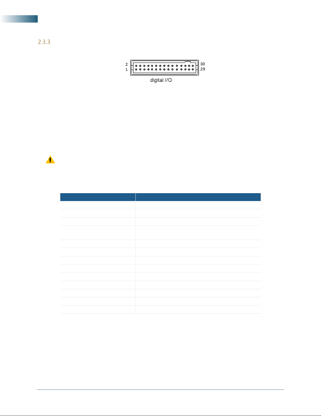
Communication and Supply Connection
Figure 3. Power and Digital IO Connector
Power and communication to the SC5320A is provided through a rectangular connector from
Samtec whose part number is TFM-115-01-L-D-RA. It also servesas the digital connector interface
for RS232/SPI, trigger, and other digital signals. With exception for the RS232 logic levels, all other
logic levels are 3.3V LVCMOS whose inputs are also 5V tolerant. A mating pig-tail cable, part
number SFSD-15-28-H-10.00-SR, is provided with the product. The pin definitions are listed in
Table 3.
Pinouts are different for different SignalCore products with the same connector type. Please
ensure that mating connectors and cables are wired correctly before connection.
Table 3. Interface connector pin out description
PIN #
Description
2,4,6,8
12V Supply Rail
12
Converter Status/Active
14
System Reset, Logic 0 to Reset Device
16
RS232 Baud Rate: 1(default) -> 115200, 0 -> 57600
SPI Mode Select: 1 (default) mode 1, 0 mode 0
17
Reserved, Pull High to 3.3V or DNC
19
Device Accessed/Active
20
LO Status/Active
24
TX for RS232 or MOSI for SPI (Host referred)
26
SPI CS_b
27
RX for RS232 or MISO for SPI (Host referred)
30
SPI CLK
9,10,13, 18,21,22
Reserved, Do Not Connect
1,3,7,11,15,23,29
GND

©2021 Rev 0.1
11
Physical Description
Figure 4. Proper Removal of Latching-Style Ribbon Connectors.
Rev 0.1 | SC5319A & SC5320A Hardware Manual SignalCore, Inc.
12
SC5319A & SC5320A Hardware Manual
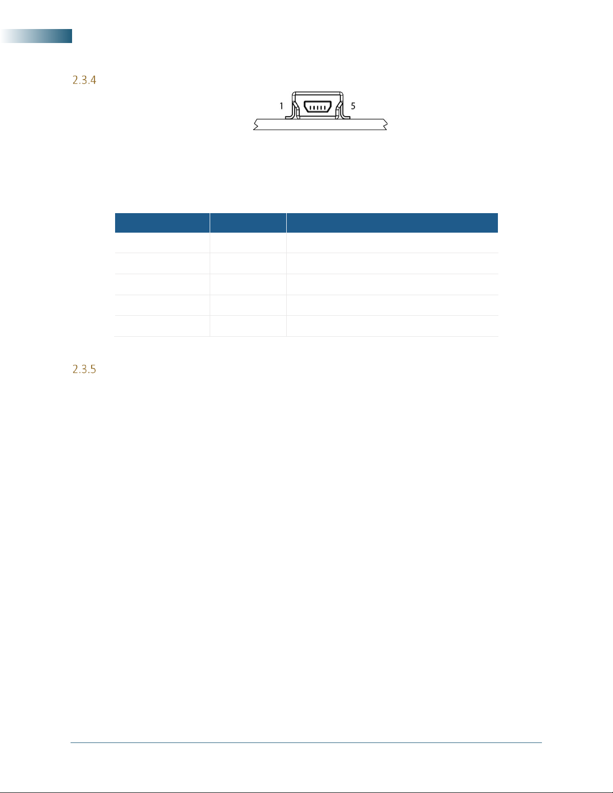
Mini-USB Connection
This is a mini-USB Type B connector for USB communication with the device using the standard
USB 2.0 protocol (full speed) found on most host computers. The pinout of this connector, viewed
from the front, is shown in the following table.
PIN #
USB Function
Description
1
VBUS
Vcc (+5 Volts)
2
D-
Serial Data (neg)
3
D+
Serial Data (pos)
4
ID
Not Used
5
GND
Device Ground (also tied to connector shell)
Reset Button (Pin Hole)
Behind this pin hole is the reset button, which is only available on the SC5320A. Using a pin to
lightly depress this momentary-action push button switch will cause a hard reset to the device,
putting it back to its default settings. All user settings will be lost. System reset capability can also
be accessed through the communication header connector.

©2021 Rev 0.1
13
Functional Description
3Functional Description
Overview
The SC5320A uses USB as its primary interface with an optional SPI or RS232 interface. The SC5319A
is a PXIe version of the product.
The downconverter assembly consists of 2 module parts:
•The Signal Conversion Module contains the mixers, filters, signal amplifiers, andattenuators. This
module is referred to as the “signal chain”. This conversion module also includes a built-in LO
synthesizer.
•The Power Conditioning and Digital Control Board contains the supply switchers that generate
the needs rails for the RF modules and an onboard MCU that provides both the computation
engine and interface between the user and the RF modules.
The figure below shows how the modules relate to each other.
Figure 5. Simplified Block Representation of the Downconverter Assembly Module
The downconverter has a single conversion stage that converts the RF signal to an intermediate
frequency (IF). The RF input range of this downconverter is from 20 GHz to 40 GHz, while the output
IF range is from 50 MHz to 5000 MHz. The LO signal needed for the conversion may be selected from
the internal synthesizer or an external signal source. The range of the LO is from 10 GHz to 20 GHz.
The frequency accuracy and stability of the internal LO is derived from an onboard Oven Controlled
Crystal Oscillator (0CXO) with an initial accuracy better than 20 ppb. For better accuracy and stability,
the synthesizer can lock to an external reference of higher precision via the Ref In port.
The Signal Chain
The conversion module contains the mixer, filters, amplifiers, and attenuators used to convert,
purify, and maintain the conversion gain of the signal between the input of the device to its output.
Signal Conversion
Supply Conditioning and Digital Control/Interface
RF Input
(K)
Ref In/Out
(SMA)
Digital IO
IF / Bypass
Output (K)
LO In/Out
(SMA)
Ref Out
(MMCX)
Synthesized Local Oscillator

Rev 0.1 | SC5319A & SC5320A Hardware Manual SignalCore, Inc.
14
SC5319A & SC5320A Hardware Manual
This cascade of signal conversion and conditioning stages is often referred to as the signal chain,
which is shown on the system block drawing of Figure 6.
The RF Input
The RF port connector is a 2.92mm (K) type rated to40 GHz of operation. The RF port is AC coupled
with a 0.1 broadband capacitor as indicated in Figure 6. The input frequency range at this port
is from ~100 kHz to 40 GHz; is full range can be switched directly to the IF port, however 20 GHz to
40 GHz signals can be converted (see 3.2.3). The usability of the upper out-of-bounds region
depends on the roll-off response of the mixer.
Figure 6. Block diagram of the downconverter assembly
The LO Input/Output
The LO input/out port connector is a SMA type. When the device is configured to use its internal
synthesizer as the LO for the mixer, this port is enabled as an output for the synthesized signal. In
other words, the device can export its LO signal out to be used by other devices. This is useful in
phase coherent multiple channel systems that uses a common LO. This port can also be configured
as an input for an external LO source; in this case the internal synthesizer is disabled and powered
down to standby.
The Input Path Switch
Immediately following the capacitor is an RF switch to selectively direct the RF signal down two
paths:
1. The default is the conversion path where the RF signal is converted to an IF.
2. The alternate path is directly to the IF output port, bypassing all means of frequency
conversion. The upper frequency limit of this bypass path is 40 GHz.
R
I
L
2
RF_PREAMP
LNA
LPF
5.0 GHz
RF_ATTEN
40 GHz DSA
dB
0.5 dB step
IF_ATTEN
6 GHz DSA
0 to 31.75 dB
.25 dB step
Referece In/Out 10 MHz
Internal LO
Synthesizer
GHz
LO Out
LO Input/out
Bypass/IF
~DC to 40 GHz
RF In
~DC to 40 GHz
50IF Amp
IF Amp
IF Amp
RF
Linear
Amp
LO
Buffer
Amp
~DC GHz Bypass
User
controlled
component
20-40 GHz conversion path
+ -
IF Filter
Settable BW
0 to 15
Referece Out
In/
Out
Out

©2021 Rev 0.1
15
Functional Description
When the conversion path is bypassed, the IF output is disabled and the internal LO is powered
down.
The RF Conversion Path
The first device in the RF conversion path is a step attenuator with 0.5 dB step resolution. This
attenuator (RF_ATTEN) is used to control the signal level at the mixer or at the RF preamplifier if it
is enabled. If the RF level at the input of these devices is relatively large with respect to their input
compression points, the signal would experience significant nonlinear effects that would distort its
waveform and produce large spurious 3rd intermodulation distortion effects.
Following RF_ATTEN is a switchable RF amplifier that can be switched into the signal path to
improve the device sensitivity, effectively lowering the device noise figure. In other words, the
effective input noise level of the device is lowered when this amplifier is enabled. When signals
with levels lower than -30 dBm are expected, turning on this amplifier is recommended to improve
the device sensitivity to these levels. The typical maximum gain of the downconverter without the
amplifier enabled is +30 dB, and when the amplifier is enabled, its additional +20 dB will boost the
typical maximum gain to approximately +50 dB.
The RF linear amplifier prior to the mixer input acts as a unity buffer to improve the reverse
transmission of signals at the mixer or created at the mixer such as the LO and IF products. Another
point to mention is there are no band selective filters in the RF path so in open environments the
device is unable to differentiate a RF signal from its image. A band select filter at the RF input port
is recommended to properly filter through the signal of interest before down conversion.
The First Mixer and IF Path
The mixer (RF mixer) of the downconverter is extremely critical as it sets the dynamic ranges of the
device, both the signal-to-noise (DRSNR) and third order IMD (DRIMD) dynamic ranges. The DRSNR and
DRIMD are directly related to the mixer input compression point (IP1dB) and input third-order
intercept point (IIP3). The IIP3 of the mixer is equivalently typically better than +12 dBm, and its
input P1dB is better than 5 dBm. In applications that require better signal linearity, it is
recommended that the level at the mixer input is kept at -20 dBm or less. Typically, the IMD is
better than -65 dBc for two -20 dBm tones at the mixer (no RF attenuation). Increasing the level at
the mixer improves SNR of the IF output signal at the expense of higher nonlinear 3rd order
byproducts.
Another important characteristic of the mixer is the LO-IF isolation and LO-RF isolation. The higher
the isolation, the lower the leakage LO signal is at the RF and IF ports. The RF mixer is driven with
a ~+17 dBm LO signal and the LO-IF isolation is about 45 dB, resulting in a -28 dBm LO leakage at
the IF terminal of the mixer, which may leak into the IF path. The low-pass IF filters suppress this
leakage to levels well below -60 dBm. The LO-RF isolation is also about 45 dB so the LO leakage at
the RF port of the mixer is on the order of -28 dBm. The high reverse isolation of the RF linear
power amplifier suppresses this LO leakage to < 60 dBm. When the low noise pre-amplifier is
enabled, it will provide another 30 dB of reverse isolation, lowering the LO leakage at the RF input
port to < 90 dBm.
The frequency relationship between the three ports of the mixer is given as:

Rev 0.1 | SC5319A & SC5320A Hardware Manual SignalCore, Inc.
16
SC5319A & SC5320A Hardware Manual
From the above equation, the IF output spectrum is inverted with respect to the RF in the first
relationship, whereas in the second it is noninverted. The former is lower sideband conversion, and
the latter is upper sideband conversion. When the LO > RF, the IF signal is inverted, and it is not
inverted when LO < RF.
Signal Chain Configurations
Recommended signal chain configurations are provided below for various application scenarios.
These are strictly recommendations. They are not indicative of the downconverter function
limitations. Users will need to adapt the device to their applications at hand.
Signals Bypassing the Conversion Stage
The RF input signal can be directed to the RF output port, bypassing the conversion process, and
handle the signal to another downconverter that might be able to cover bands outside of the
device range. For example, the SC5318A downconverter mates well with this device to form an
integrated converter with continuous frequency coverage from 6 GHz to 40 GHz.
Dynamic Range Setting
There are 2 digital step attenuators to control the conversion gain of the downconverter. The first
set consists of RF_ATTEN in the RF stage and the second set consists of IF_ATTEN in the IF stage.
Both attenuators have 30 dB of settable range, however the IF attenuator has fine resolution of
0.25 dB while the RF attenuator has resolution of 0.5 dB.
To set the downconverter for better sensitivity or better SNR, the gain should be shifted to the
RF input path of the device before themixer. The RF pre-amplifier should be enabled if necessary
and/or RF attenuation reduced. The IF attenuator is then used to adjust the final IF output level.
The drawback is that the signal level starts off higher as it enters the first mixer as well as the
subsequent components so, as a result, the apparent linearity of the device is lower.
To set the device for better linearity, the gain should be shifted to the output IF path (after the
mixer) and reduced in the RF path. The signal power level at the input should be lower than -20
dB for improved linearity. Since the input signal is low, the relative SNR will be lowered too. But,
as the first mixer and subsequent components experience lower power levels, the apparent
linearity of the device is improved at the expense of a lower SNR dynamic range.
When the device gain is balanced well, the device could achieve SNR better than 130 dBc/Hz
while maintaining IMD3 levels close to 68 dBc. These numbers are representative of converters
used in large box high end spectrum analyzers. When the deviceis optimized for best SNR, typical
values greater than -150 dBc/Hz can be achieved, and when the device is optimizedfor sensitivity
by enabling the RF preamplifier, the input spectral noise floor is typically lower than -165 dBm/Hz.
The flexible use of these attenuators and pre-amplifier allows the downconverter to achieve
better than 190 dB of measurement dynamic range.

©2021 Rev 0.1
17
Functional Description
The LO Synthesizer
The internal LO synthesizer is a hybrid between integer-N PLL and DDS, enabling it to tune at 1 Hz
steps while maintaining low phase noise. The master reference signal for the generation of the LO
signal comes either from an internal Oven Controlled Crystal Oscillator (OCXO) or an external signal
source as shown below in Figure 7. The colored blocks indicate that they are user controllable via
software. The frequency range of the synthesizer is 10 to 20 GHz, which is frequency doubled to
drive the mixer LO port.
Figure 7. Block diagram of the local oscillator
The Reference Clocks
The internal base clock of the downconverter is a 10 MHz Voltage Controlled Oven Controlled
Crystal Oscillator (VCOCXO) with initial accuracy better than 20 ppb once the device has reached a
stable temperature. Its initial accuracy is set at the factory via an on-board 14-bit voltage reference
DAC. This DAC is accessible for dynamic accuracy calibration. The other reference is a 100 MHz
Voltage Controlled Crystal Oscillator (VCXO),which is phase locked to this base reference whenever
an external reference source is not used.
When an external reference is selected as the base clock, by enabling the device to phase lock to
it, the device will only attempt to lock when the presence of a reference signal is detected at the
input port. This sets the device to “phase lock on detection”. Notice that both the reference clocks
(OCXO and VCXO) will attempt to lock to the external source to ensure there always is only one
base frequency source. If an external source is not used, its connection should physically be
removed from the input port to avoid the device from picking on its signal as this could produce
unwanted offset spurious effects. Having the VCXO lock directly to the external source has the
advantage of utilizing the close-in phase noise of the source; this is assuming the external source
phase noise is superior to the internal base. Finally, although the internal VCOCXO is not used when
an external reference is selected, it remains powered on and locked to maintain its frequency
coherence and temperature stability.
The Reference Ports
There are 2 reference ports on this device, first there is a SMA type connector whose main purpose
is to receive an external reference signal. However, it can be programmed as an output of the
internal OCXO reference signal. The other is a MMCX type connector that is always active as an
output.
VCXO PLL
REF DETECT
Enable
Ext Lock
LO
OCXO PLL
Ref
In/Out
To
Mixer
LO
Ref Out
Enable Ref Out
MMCX
LO
In/Out
2
Enable
LO In
DAC

Rev 0.1 | SC5319A & SC5320A Hardware Manual SignalCore, Inc.
18
SC5319A & SC5320A Hardware Manual
LO Port
The LO port is bi-directional; it may be programmed either as an input or output. The frequency
range is 10 GHz to 20 GHz.
The Interface Module
The following figure shows the power and control interface block for the device. All supply rails are
produced on board; their voltages are regulated and actively filtered to keep noise to a minimum.
Thus, these downconverters are tolerant to “dirty” external power supplies.
Figure 8. Block diagram of the power and interface module
+18V, +10V, +5V, +3.3V,
-5V, -10V
To LO & SignalChain Module
MCU
Switchers and regulators
PXI Power PXIe Interface
Ext.Power
+12V USB RS232,
SPI
PXIe-Serial
Bridge
SC5319A
SC5320A

©2021 Rev 0.1
19
Hardware Registers
4Hardware Registers
The set of hardware registers of the downconverter may be divided into a configuration set and a
query set; the configuration registers are write-only registers to set up the states of the device, while
the query registers request the device to prepare and send back data associated with them. The
registers are identical for all communication interfaces: PXIe, USB, RS232, and SPI. Data
communication to all interfaces are sent in 1 byte wide, that is, data is transferred byte-by-byte.
Register data lengths vary in size, and it is important that the correct number of bytes are sent for the
corresponding register. Failure to do so may cause communication to lock-up and the device to
become unresponsive.
Configuration Registers
These are write-only registers to configure the device. The registers vary in length to reduce
redundant data and improve the communication speed, especially for SPI and RS232 interfaces.
Furthermore, it is vitally important that the length of data written to a register is exact because
failure to do so will cause the interfaces to misinterpret the incoming data, leaving the device in a
stalled state. The total number of bytes is the sum of the register address (1 Byte) and its
corresponding data bytes. For example, to set the RF frequency value, eight bytes must be written;
the sum of the1 register byte and 7 data bytes. See theRF_FREQUENCY register of Table 5. The table
provides a summary of the configuration registers, and each register is explained in detail.
Table 4. Configuration Registers
Register Name
Reg Add
Serial
Range
Bit 7
Bit 6
Bit 5
Bit 4
Bit 3
Bit 2
Bit 1
Bit 0
INITIALIZE
0x01
[7:0]
Set to zeros [7:1]
Mode
SYSTEM_ACTIVE
0x02
[7:0]
Set to zeros [7:1]
Enable “active” LED
SYNTH_MODE
0x03
[7:0]
Set to zeros [7:2]
Fast-tune
Loop Gain
RF_FREQUENCY
0x10
[7:0]
Frequency Word (Hz) [7:0]
[15:8]
Frequency Word (Hz) [15:8]
[23:16]
Frequency Word (Hz) [23:16]
[31:24]
Frequency Word (Hz) [31:24]
[39:32]
Frequency Word (Hz) [39:32]
[47:40]
Frequency Word (Hz) [47:40]
[55:48]
Frequency Word (Hz) [55:48]
IF_FREQUENCY
0x11
[7:0]
Frequency Word (Hz) [7:0]
[15:8]
Frequency Word (Hz) [15:8]
[23:16]
Frequency Word (Hz) [23:16]
[31:24]
Frequency Word (Hz) [31:24]
[39:32]
Frequency Word (Hz) [39:32]
[47:40]
Frequency Word (Hz) [47:40]
[55:48]
Frequency Word (Hz) [55:48]
LO_FREQUENCY
0x12
[7:0]
Frequency Word (Hz) [7:0]
[15:8]
Frequency Word (Hz) [15:8]
[23:16]
Frequency Word (Hz) [23:16]
[31:24]
Frequency Word (Hz) [31:24]
[39:32]
Frequency Word (Hz) [39:32]
[47:40]
Frequency Word (Hz) [47:40]
[55:48]
Frequency Word (Hz) [55:48]
LO_SOURCE
0x14
[7:0]
Set to zeros [7:1]
Ext
RF_AMP
0x14
[7:0]
Set to zeros [7:1]
Enable
ATTENUATOR
0x15
[7:0]
Attenuator Value
This manual suits for next models
1
Table of contents
Other SIGNALCORE Media Converter manuals


Popular Media Converter manuals by other brands


IMC Networks
IMC Networks MediaConverter/1 Declaration of conformity

AMX
AMX Video Decoder MAX-CSD10 Dimensions

Stello
Stello DA220 owner's manual

Baumer
Baumer HOG 165 + DSL Mounting and operating instructions

Advance acoustic
Advance acoustic RCE/100-2E-3 Operation manual

Allied Telesis
Allied Telesis DMC1000/100 Series installation guide


