SiTime SiT92216 User manual

SiT92216EB User Manual | Rev 0.5
Page 1 of 27
www.sitime.com
SiT92216 Evaluation Board (EVB) HW
User Manual
Table of Contents
1Introduction ......................................................................................................................................................................... 1
2Features.............................................................................................................................................................................. 1
3Functional Description......................................................................................................................................................... 2
3.1. VDD and VDDO Power Supplies...............................................................................................................................2
3.2. Clock Inputs...............................................................................................................................................................2
3.3. Clock States (Input vs Output States)........................................................................................................................1
3.4. Output Driver Type....................................................................................................................................................1
3.5. Reference Output......................................................................................................................................................1
4Power Supply Connections................................................................................................................................................. 2
5Setting Input Clock Select and REF Out Enable in the EVK ............................................................................................... 4
6Input Clock Configuration.................................................................................................................................................... 5
7Configuring for Single ended AC coupled Input Clock ........................................................................................................ 6
7.1. Driving Clock Inputs with LVCMOS Driver (AC coupled)...........................................................................................6
7.2. Driving Clock Inputs with LVCMOS Driver (DC coupled)...........................................................................................7
8Driving Differential LVDS or LVDS Boost (AC coupled)...................................................................................................... 9
8.1. Board Configuration for driving DC Coupled LVDS...................................................................................................9
9Board Configuration Required for Driving DC/AC coupled LVPECL................................................................................. 10
9.1. DC/AC Coupled LVPECL........................................................................................................................................10
10 Output Configuration......................................................................................................................................................... 11
11 EVB Snapshot................................................................................................................................................................... 12
12 Schematics of SiT92216 Evaluation Kit............................................................................................................................. 13
12.1. Schematic Sheet 1 ................................................................................................................................................13
12.2. Schematic Sheet 2 ................................................................................................................................................14
12.3. Schematic Sheet 3 ................................................................................................................................................15
12.4. Schematic Sheet 4 ................................................................................................................................................16
12.5. Schematic Sheet 5 ................................................................................................................................................17
12.6. Schematic Sheet 6 ................................................................................................................................................18
12.7. Schematic Sheet7 .................................................................................................................................................19
12.8. Schematic Sheet8 .................................................................................................................................................20
12.9. Schematic Sheet9 .................................................................................................................................................21
12.10. Schematic Sheet10 ............................................................................................................................................. 22
12.11. Schematic Sheet11 ............................................................................................................................................. 23

SiT92216 Evaluation Board (EVB) HW User Manual
SiT92216EB User Manual | Rev 0.5
Page 1 of 27
www.sitime.com
1 Introduction
The SiT92216 Evaluation Board is designed for evaluating the SiT92216, is a 4 differential output and 1 LVCMOS ultra low-jitter
clock fan-out buffer.
Figure 1. SiT92216 EVB Board
2 Features
1) Additive jitter performance of 50 fs RMS.
2) 3:1 input clock selection.
3) Two universal clock inputs can operate up to 2.1 GHz and accept LVPECL, LVDS, LVCMOS, CML, HCSL, SSTL or
single ended clocks.
4) One crystal input which can support crystals in the frequency range of 8 MHz to 50 MHz or it can accept single ended
input clock.
5) Two output driver banks A and B which can be programmed independently to LVPECL, LVDS, HCSL or HIZ mode.
6) Typical output skew between clock outputs is 30 ps.
7) Level translation with core supply voltage of 3.3 V/2.5 V/1.8 V and 3.3 V/2.5 V/1.8 V output supply for differential output
drivers.
8) SiT92216 buffer is pin controlled.
9) High PSRR -70/-73 dBc for LVPECL/LVDS modes.
SiT92216 Evaluation Board (EVB) HW User Manual
SiT92216EB User Manual | Rev 0.5
Page 2 of 27
www.sitime.com
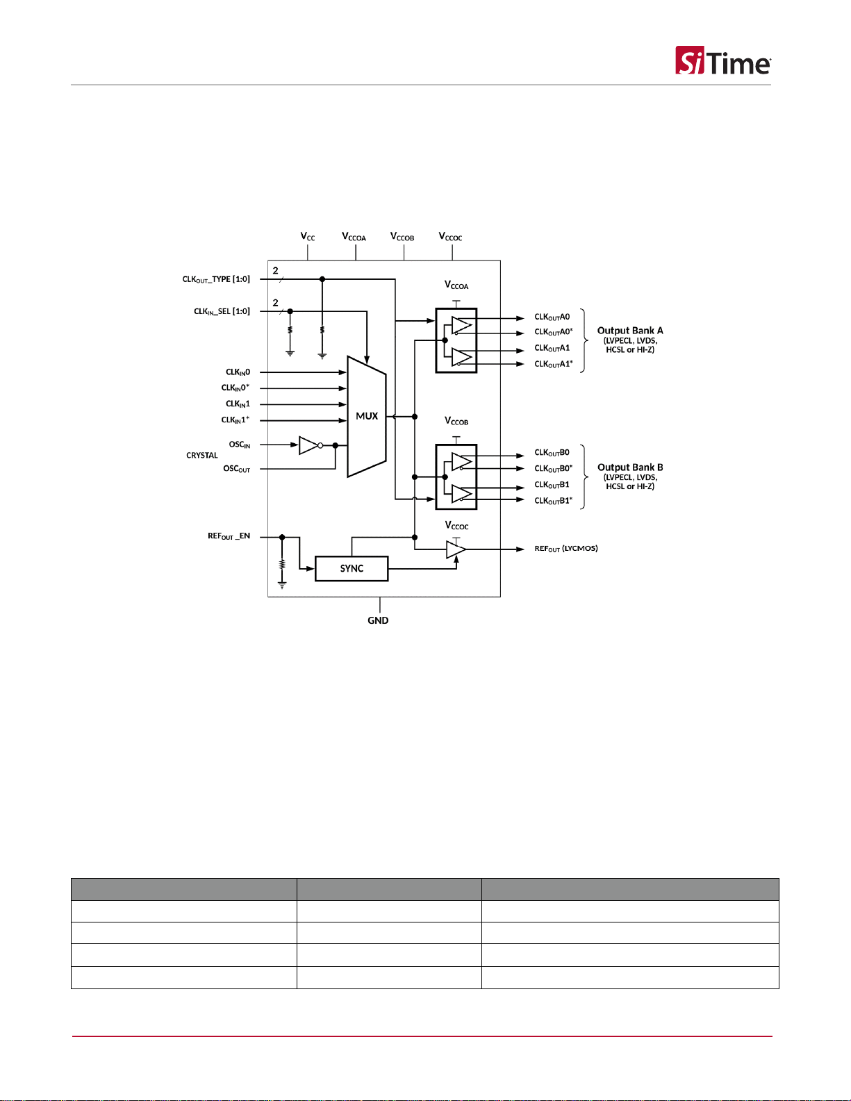
3 Functional Description
The SiT92216 is a 4 differential output and 1 LVCMOS output clock fan out buffer with low additive jitter that can operate up to
2.1 GHz. It features a 3:1 input multiplexer with an optional crystal oscillator input, two banks of 2 differential outputs with multi-
mode buffers (LVPECL, LVDS, HCSL, or Hi-Z), one LVCMOS output, and 3 independent output buffer supplies. The input
selection and output buffer modes are controlled via pin strapping. The device is offered in a 32-pin QFN package.
Figure 2. Functional Diagram
3.1. VDD and VDDO Power Supplies
The SiT92216 has separate 3.3/2.5/1.8 V core (VCC) and 3 independent 3.3 /2.5/1.8 V output power supplies (VCCOA,
VCCOB, and VCCOC) supplies. Output supply operation at 2.5/1.8 V enables lower power consumption and output-level
compatibility with 2.5/1.8 V receiver devices. The output levels for LVPECL (VOH, VOL) and LVCMOS (VOH) are referenced to
its respective VCCO supply, while the output levels for LVDS and HCSL are relatively constant over the specified VCCO range.
3.2. Clock Inputs
The input clock can be selected from CLKin0/CLKin0*, CLKin1/CLKin1*, or OSCin. Clock input selection is controlled using the
CLKin_SEL[1:0] inputs as shown in Table 1. When CLKin0 or CLKin1 are selected, the oscillator is power down. The user can
float OSCin and OSCout pins, since these pins are internally pulled down. OSCin is pulled down with a 56 KOhm resistance.
Table 1. Input Clock Selection
CLKin_SEL[1]
CLKin_SEL[0]
Selected Clock
0
0
CLK0
0
1
CLK1
1
0
Crystal Or Crystal bypass AC coupled mode
1
1
Crystal bypass DC coupled mode
SiT92216 Evaluation Board (EVB) HW User Manual
SiT92216EB User Manual | Rev 0.5
Page 1 of 27
www.sitime.com
3.3. Clock States (Input vs Output States)
Table 2. Input versus Output Stages
State of Selected Clock input
Output State
Inputs are floating
Logic low
Inputs are logic low
logic low
Inputs are logic high
logic high
3.4. Output Driver Type
The differential output buffer type for Bank A and Bank B outputs can be configured using the CLKout_TYPE[1:0] inputs, as
shown Table 3. For applications where all differential outputs are not needed, any unused output pin should be left floating with
a minimum copper length to minimize capacitance and potential coupling and reduce power consumption. If an entire output
bank will not be used, it is recommended to disable (Hi-Z) the bank to reduce power.
Table 3. Programming of Output Driver Type
CLKOUT_TYPE1
CLKOUT_TYPE0
CLK Buffer Type
0
0
LVPECL
0
1
LVDS
1
0
HCSL
1
1
HIZ
3.5. Reference Output
The reference output (REFout) provides a LVCMOS copy of the selected input clock. The LVCMOS output high level is
referenced to the VCCOC voltage. REFout can be enabled or disabled using the enable input pin, REFout_EN, as shown in Table
4.The reference output clock is internally synchronized to the selected clock. This avoids any glitches or runt pulses while
enabling or disabling the reference clock.
When REFout_EN goes from low to high, the output clock is enabled within a time delay td, where td is given by the following
equation.
. Tin is the time period of the input clock.
Table 4. Reference Output Enable
Refout_EN
Output State
0
Disabled (HiZ)
1
Enabled

SiT92216 Evaluation Board (EVB) HW User Manual
SiT92216EB User Manual | Rev 0.5
Page 2 of 27
www.sitime.com
4 Power Supply Connections
SiT92216 buffer has four suuplies VCC, VCCOA, VCCOB and VCCOC. The VCCOA supply is dedicated supply for the bank A
output drivers. The VCCOA supply can be 3.3 V+/-5%, 2.5 V+/-5%, 1.8 V+/-5%. The VCCOB supply is dedicated supply for the
bank B output drivers. The VCCOB supply can be 3.3V+/-5%, 2.5 V+/-5%, 1.8 V+/-5%. The VCCOC supply is dedicated supply
for the LVCMOS output driver. The VCCOC supply can be 3.3 V+/-5%, 2.5 V+/-5%, 1.8 V+/-5%. The VCC supply is dedicated
for the input clock receiver, clock distribution unit and the XO inside SiT92216. This supply is independent of VCCOA, VCCOB,
VCCOC. The VCC supply can vary from 3.3 V+/-5%, 2.5 V+/-5%, and 1.8 V +/- 5%.
The VCC, VCCOA, VCCOB, VCCOB supplies can be set as per the Table 5.
Table 5. Power supply connection for SiT92216 evaluation kit
Power Source
Jumper setting
Comments
PC/laptop USB port
J5 shorted between pins 1,2
Default EVK configuration
Single External Source of 5V
J5 shorted between pins 2,3
Note: Refer Figure 17. Schematic Sheet 5 VDD_AUX regulator for jumper J5 connection
after connecting the USB. SiT92216
can be programmed to different voltage levels using jumper settings as shown in Table 6.
Table 6. Setting VCC voltage
LDO
Jumper setting
VCC (V)
U1
J2 shorted between pins 2,3
3.3
J2 shorted between pins 1,2
2.5
J2 left open
1.8
Note:
1. Refer Figure 13. Schematic Sheet 1 VCC Regulator for Jumper J2 connection.
2.
Table 7. Setting VCCOA voltage
LDO
Jumper setting
VCCOA (V)
U2
J9 left open
3.3
J9 shorted between pins 1,2
2.5
J9 shorted between pins 2,3
1.8
Note:
1. Refer Figure 14. Schematic Sheet 2 VCCOA regulator for Jumper J9 connection.
2.
Table 8. Setting VCCOB voltage
LDO
Jumper setting
VCCOB (V)
U3
J11 left open
3.3
J11 shorted between pins 1,2
2.5
J11 shorted between pins 2,3
1.8
Note:
1. Refer Figure 15. Schematic Sheet 3 VCCOB regulator for Jumper J11 connection.
2. .

SiT92216 Evaluation Board (EVB) HW User Manual
SiT92216EB User Manual | Rev 0.5
Page 3 of 27
www.sitime.com
Table 9. Setting VCCOC voltage
LDO
Jumper setting
VCCOC (V)
U4
J14 shorted between pins 2,3
3.3
J14 shorted between pins 1,2
2.5
J14 left open
1.8
Note:
1. Refer Figure 16. Schematic Sheet 4 VCCOC regulator for Jumper J11 connection.
2.
Table 10. Setting VCC_AUX voltage
LDO
Jumper setting
VCC_AUX (V)
U8
J56 shorted between pins 2,3
3.3
J56 shorted between pins 1,2
2.5
J56 left open
1.8
Note:
1. Refer Figure 17. Schematic Sheet 5 VDD_AUX regulator for Jumper J56 connection.
2. VCC_AUX is the supply of level shifter outputs for automated control of clock select, REFOUT_EN pins, ODR type. Keep VCC = VCC_AUX
3. VCC_AUX is set to 3.3V using U8 L.

SiT92216 Evaluation Board (EVB) HW User Manual
SiT92216EB User Manual | Rev 0.5
Page 4 of 27
www.sitime.com
5 Setting Input Clock Select and REF Out Enable in the EVK
The jumper setting for controlling the input clock select and output enable are given below.
Table 11. Jumper settings to control clock select, ODR type change and REF out enable
Pin
Jumper state
Logic input
CLK_IN_SEL0
J67 shorted between 2,3
0
J67 shorted between 1,2
1
CLK_IN_SEL1
J68 shorted between 2,3
0
J68 shorted between 1,2
1
REF_OUT_EN
J71 shorted between 2,3
0
J71 shorted between 1,2
1
CLK_OUT_TYPE1
J22 shorted between 2,3
0
J22 shorted between 1,2
1
CLK_OUT_TYPE0
J60 shorted between 2,3
0
J60 shorted between 1,2
1
Note:
1. The programming for input clock select is given below.
2. Input clock select programming: 2'b00 - clock0, 2'b01 - clock1, 2'b10 XO
3. The programming for REF_OUT_EN is given below
a) REF_OUT_EN programming: 1'b0 - output disable, 1'b1 - output enable
4. Refer Figure 20. Schematic Sheet 8 FTDI signal to DUT mapping for Jumper J71 connection.
5. The programming for odr type for A and B bank is given below.
a) ODRA type programming : 2'b00 - LVPECL, 2'b01 - LVDS, 2'b10 - HCSL, 2'b11 HI
b) Refer Figure 20. Schematic Sheet 8 FTDI signal to DUT mapping for Jumper J22, J60 connection.
6. Jumpers labelled as JVDD1, JVDD2, JVDD3, Diag should be left in their default state: floating.
7. J8 should remain in the default state: between pin1 and pin2 t

SiT92216 Evaluation Board (EVB) HW User Manual
SiT92216EB User Manual | Rev 0.5
Page 5 of 27
www.sitime.com
6 Input Clock Configuration
The input clock is ac coupled and terminated with differential 100 Ohms. Thus the EVK is configured for differential input clock
as shown in schematic sheet9. The clock is ac coupled to the chip clock input pins.
Figure 3. Input clock configuration
SiT92216 Evaluation Board (EVB) HW User Manual
SiT92216EB User Manual | Rev 0.5
Page 6 of 27
www.sitime.com
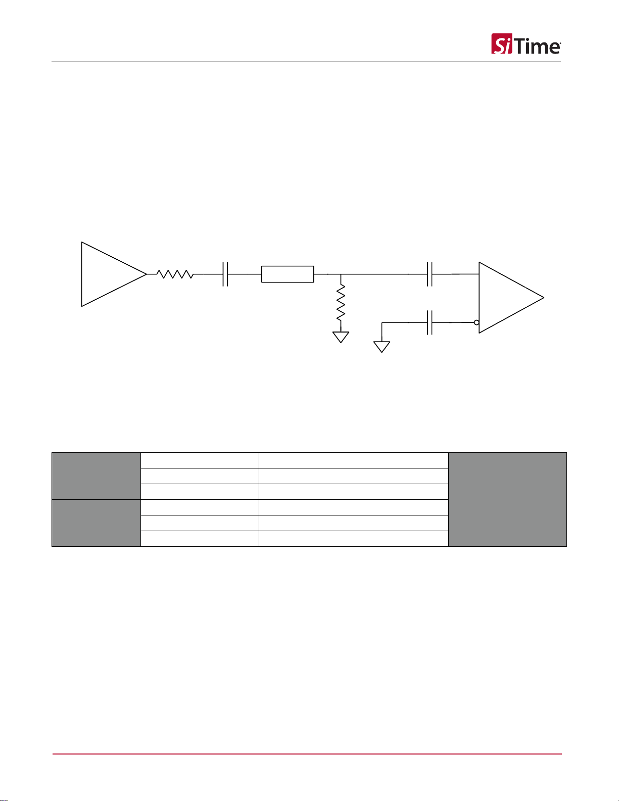
7 Configuring for Single ended AC coupled Input Clock
Many applications require the buffer to receive single ended input clock. Therefore, some minimal changes need to be done to
the EVK to accomplish single ended operation.
7.1. Driving Clock Inputs with LVCMOS Driver (AC coupled)
For large single-ended input signals, such as 3.3 V or 2.5 V LVCMOS, a 50 load resistor should be placed near the input for
signal attenuation to prevent input overdrive as well as for line termination to minimize reflections. The single-ended input slew
rate should be as high as possible to minimize performance degradation. The clock input has an internal bias voltage of about
(VDD-0.3)/2 V, so the input can be AC coupled as shown in Figure 4. The output impedance of the LVCMOS driver plus Rs
to match the characteristic impedance of the transmission line and load termination.
Figure 4 Single ended LVCMOS input, AC coupling
The board changes are listed in the table given below:
Table 12. Board component changes required to support single ended AC coupled LVCMOS
Clock 0 path
R37
change to 0.1uF
Schematic Sheet 9
C29
change to 0 Ohms
R29
change to 0 Ohms
Clock 1 path
R35
change to 0.1uF
C27
change to 0 Ohms
R30
change to 0 Ohms
SiT92216 Evaluation Board (EVB) HW User Manual
SiT92216EB User Manual | Rev 0.5
Page 7 of 27
www.sitime.com
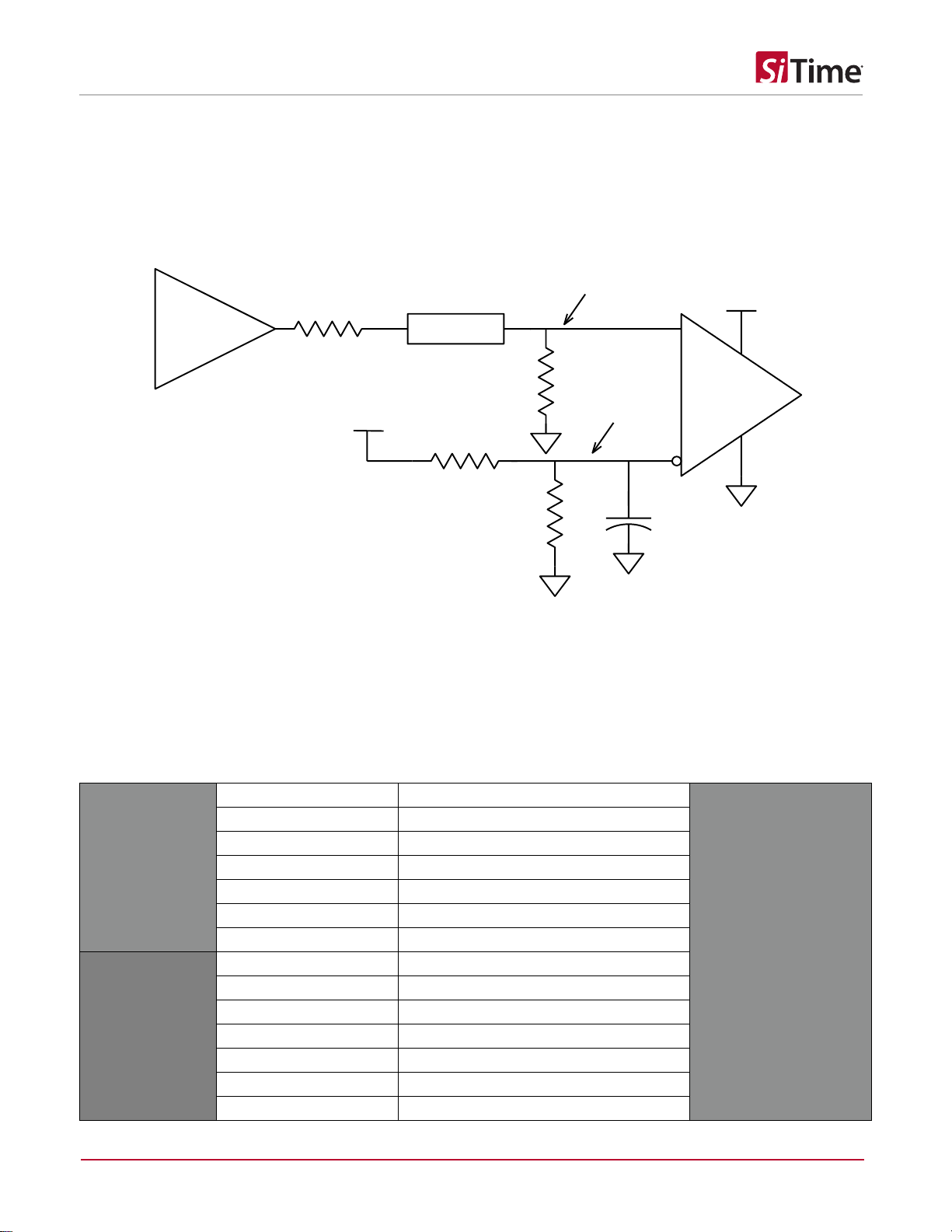
7.2. Driving Clock Inputs with LVCMOS Driver (DC coupled)
Single ended clocks can be DC coupled to the SiT92216 Buffer. If the CLKin is driven CLKin* voltage must be set using a resistor
divider to match the common mode of the DC coupled single ended clock. This is shown in Figure 5.
Figure 5. Single ended LVCMOS input, DC coupling
Case1: Let us look at the case where a LVCMOS driver (of 50 Ohm impedance) drive a 50 Ohm load which is located at the
input of SiT92216. Let the supply of LVCMOS driver be 1.8 V. Then the swing of the clock at the chip input is 0.9Vpp. We to set
the reference voltage at the reference node at 0.45 V. Choose VCC = 1.8 V, Rs2=3Rs1. Rs1, Rs2 should be in the kilo ohm
range. So if we set Rs1=3 K, Rs2=1 K.
Table 13. EVK board changes required to support single ended DC coupled LVCMOS
Clock 0 path
R29
remove
Schematic Sheet 9
C23
change to 0 Ohms
R23
change to 3KOhms
R27
change to 1K Ohms
C25
populate with 0.1uF
C32
change to 0 Ohms
C29
change to 0 Ohms
Clock 1 path
R30
remove
C24
change to 0 Ohms
R24
change to 3KOhms
R28
change to 1K Ohms
C26
populate with 0.1uF
C31
change to 0 Ohms
C27
change to 0 Ohms
SiT92216 Evaluation Board (EVB) HW User Manual
SiT92216EB User Manual | Rev 0.5
Page 8 of 27
www.sitime.com
Case2: If load is purely capacitive, let the supply of LVCMOS driver be 1.8 V. Then the swing of the clock at the chip input is 1.8
Vpp. We to set the reference voltage at the reference node at 0.9 V. Choose VCC = 1.8V, Rs2=Rs1. Rs1, Rs2 should be in the
kilo ohm range. So if we set Rs1=1K, Rs2=1 K.
Figure 6. Single ended LVCMOS input, DC coupling Capacitive load
Table 14. Single ended DC coupling for driving pure capacitive load
Clock 0 path
R29
remove
Schematic Sheet 9
R34
remove
C23
change to 0 Ohms
R23
change to 1K Ohms
R27
change to 1K Ohms
C25
populate with 0.1uF
C32
change to 0 Ohms
Clock 1 path
R30
remove
R31
remove
C24
change to 0 Ohms
R24
change to 1K Ohms
R28
change to 1K Ohms
C26
populate with 0.1uF
C31
change to 0 Ohms
SiT92216 Evaluation Board (EVB) HW User Manual
SiT92216EB User Manual | Rev 0.5
Page 9 of 27
www.sitime.com
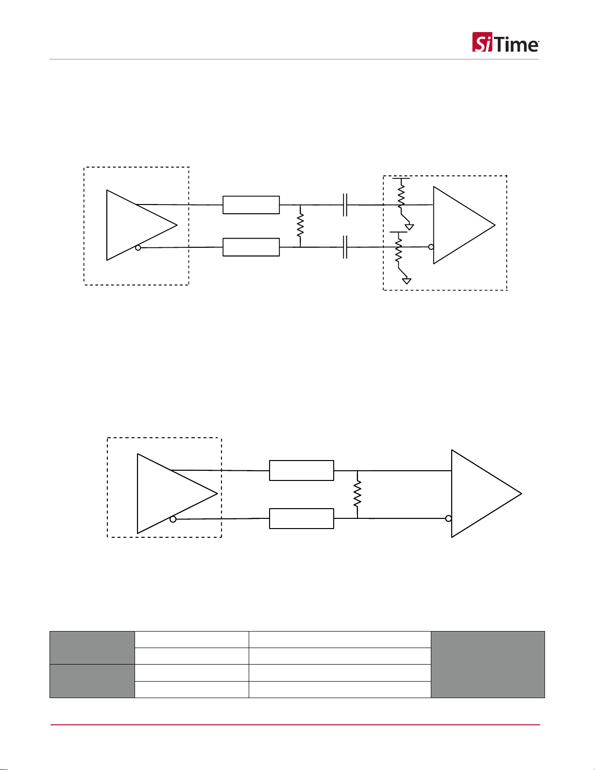
8 Driving Differential LVDS or LVDS Boost (AC coupled)
The input sees a 100 Ohm differential resistance which gives a current path for LVDS or LVDS boost. The 100 Ohm differential
signal is followed by AC coupling capacitor of 0.1 uF. So no change in board configuration is required.
Figure 7. LVDS or LVDS Boost AC coupled
8.1. Board Configuration for driving DC Coupled LVDS
LVDS (DC coupled)
Terminate with a differential 100 Ohm as close to the receiver as possible. This is shown in Figure 8.
Figure 8. Termination scheme for DC coupled LVDS
Board Changes Required for DC Coupled LVDS
Table 15. Board changes required for DC coupled LVDS or LVDS Boost
Clock 0 Path
C23
change to 0 Ohms
Schematic Sheet 9
C32
change to 0 Ohms
Clock 1 Path
C24
change to 0 Ohms
C31
change to 0 Ohms
SiT92216 Evaluation Board (EVB) HW User Manual
SiT92216EB User Manual | Rev 0.5
Page 10 of 27
www.sitime.com
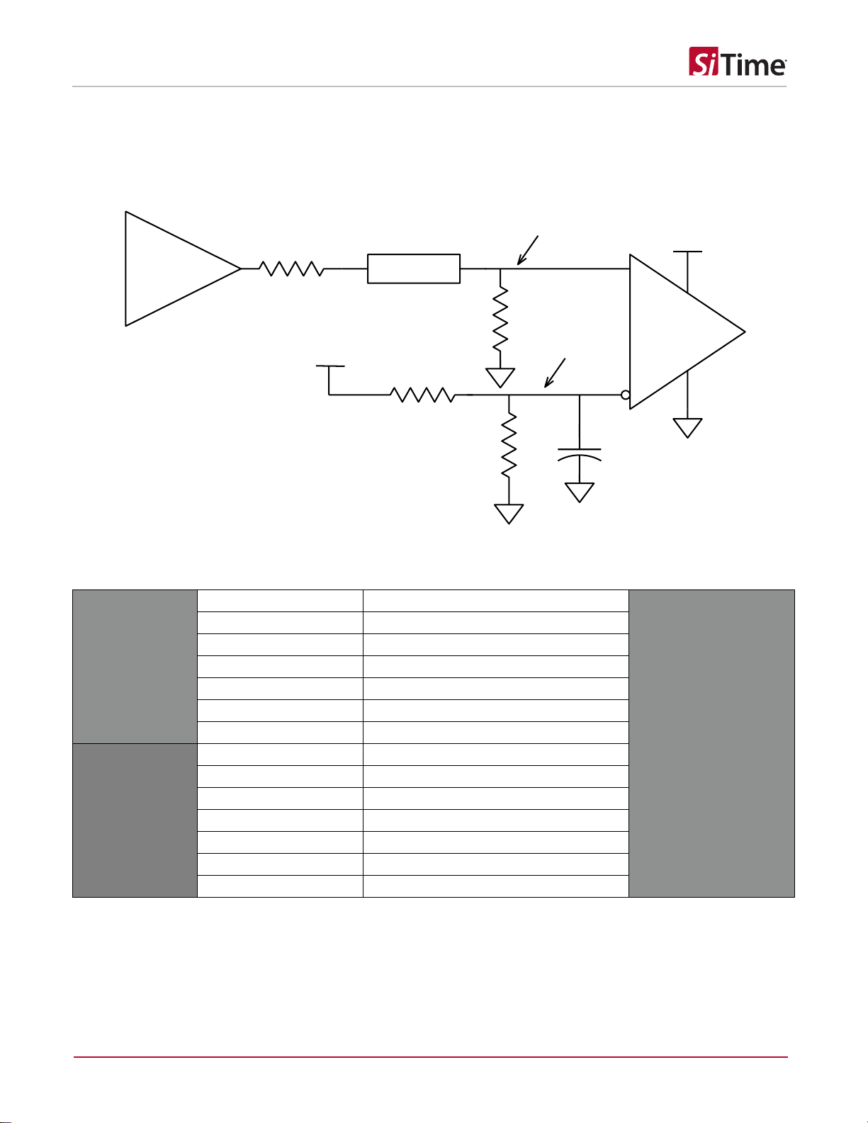
9 Board Configuration Required for Driving DC/AC coupled LVPECL
9.1. DC/AC Coupled LVPECL
The LVPECL standard requires a DC path for the input clock driver. The 50 Ohm termination at the receiver is biased with
VCCO-2 V. The VCM (VCC-2 V) need to be capable of sinking or sourcing current. There is a provision to provide VCM in the
input clock circuit through jumper J4, J7.
So no board changes are required but just give VCM through jumpers J4, J7.
Figure 9. DC coupled LVPECL

SiT92216 Evaluation Board (EVB) HW User Manual
SiT92216EB User Manual | Rev 0.5
Page 11 of 27
www.sitime.com
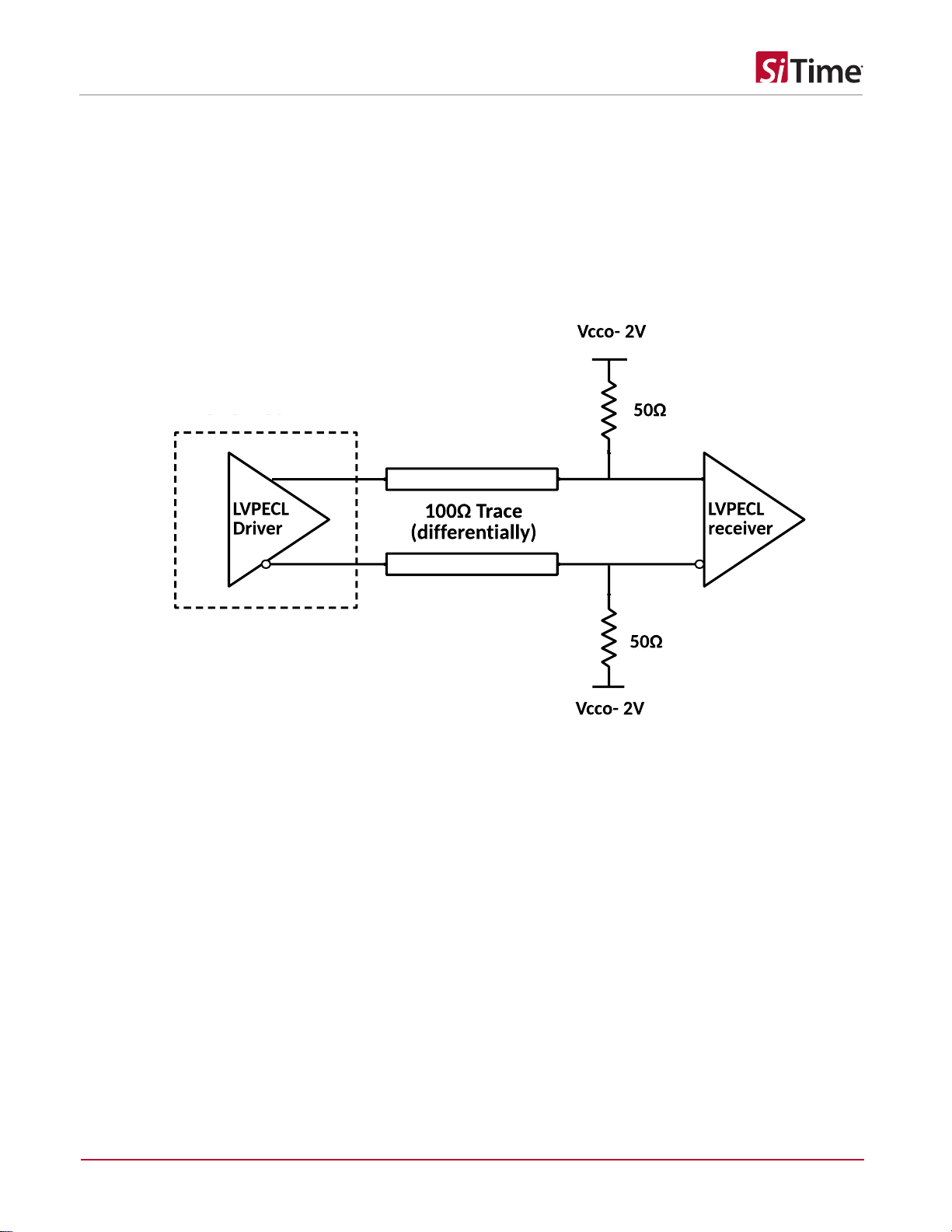
10 Output Configuration
The bank A and B outputs are by default configured for driving LVDS on the EVB. The bank A and B outputs are connected to
the SMA output connectors via a differential transmission line and 0.1uF ac coupling capacitor. Appropriate differential 100 Ohm
termination should be given for using LVDS configuration.
Figure 10. Bank A output configuration for LVDS
Figure 11. Bank B output configuration for LVDS

SiT92216 Evaluation Board (EVB) HW User Manual
SiT92216EB User Manual | Rev 0.5
Page 12 of 27
www.sitime.com
11 EVB Snapshot
Figure 12. EVB Snapshot
Block 1 has USB port to power up the board or to select jumper for power up using external supply as mentioned in Table 5.
Block 2 has jumper settings to configure chip VCC as mentioned in Table 6.
Block 3 has jumper settings to configure chip VAUX as mentioned in Table 10.
Block 4 has jumper settings to configure chip VCCOA as mentioned in Table 7.
Block 5 has jumper settings to configure chip VCCOB as mentioned in Table 8.
Block 6 has jumper settings to configure chip VCCOC as mentioned in Table 9
Block 7 has jumper settings to select CLK_IN_SEL0, CLK_IN_SEL1 and CLK_OUT_TYPE0 as mentioned in Table 11.
Block 8 has jumper settings to select REFOUT_EN as mentioned in Table 11.
Block 9 has jumper settings to select CLK_OUT_TYPE1 as mentioned in Table 11.


Table of contents
Other SiTime Motherboard manuals

SiTime
SiTime SiT6098EBB User manual

SiTime
SiTime SiT6731EB User manual

SiTime
SiTime SiT6502EB User manual

SiTime
SiTime Time Machine II User manual

SiTime
SiTime Time Machine II User manual

SiTime
SiTime SiT6731EB User manual

SiTime
SiTime SiT6722EB User manual

SiTime
SiTime SiT6098EBB User manual

SiTime
SiTime SiT6722EB User manual

SiTime
SiTime SiT6760EB User manual


