SiTime SiT6722EB User manual

SiT6722EB UM Rev 3.0
Page 1 of 8
www.sitime.com
SiT6722EB Evaluation Board User Manual
SiT6722EB Evaluation Board User Manual
Contents
1 Introduction .............................................................................................................................................1
2 I/O Descriptions .......................................................................................................................................2
3 EVB Usage Descriptions ...........................................................................................................................2
3.1 EVB Configurations........................................................................................................................2
3.1.1 I2C Support .......................................................................................................................3
3.2 Waveform Capturing Using Active Probe .....................................................................................3
3.3 Measuring Jitter and Phase Noise.................................................................................................4
3.4 Current Measurement ..................................................................................................................4
Appendix A....................................................................................................................................................5
1Introduction
The SiT6722EB evaluation board (EVB) is designed for use with SiTime’s Elite Super-TCXOs in the 10-pin,
5.0x3.2 mm ceramic packages. It enables the evaluation of key functionalities of these precision Super-
TCXOs in three configuration modes: TCXO, VCTCXO and DCTCXO with I2C.
EVB Features
-Support for three Super-TCXO configuration modes: TCXO, VCTCXO, DCTCXO
-Direct SMA outputs for frequency/jitter measurements
-Probing points for waveform measurements
-Connector access for controlling the output frequency via I2C
SiTime typically ships the EVB with the Super-TCXO mounted using SiTime recommended reflow profile.
The Super-TCXO device should only be evaluated in its original soldered down state for best signal
integrity and frequency stability. The device performance is not guaranteed if it is de-soldered and then
re-soldered either manually or via reflow process.
SiT6722EB UM Rev 3.0
Page 2 of 8
www.sitime.com
SiT6722EB Evaluation Board User Manual
2I/O Descriptions
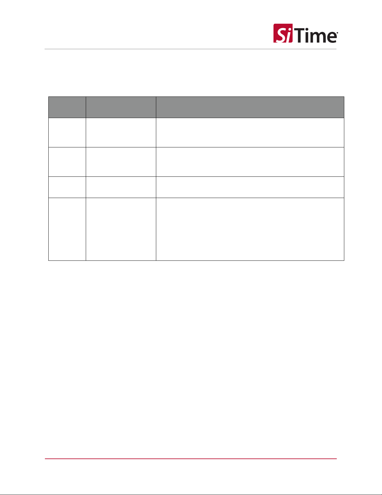
Table 1. SiT6722EB I/O
Connector
designator
I/O
Description
P1
Power Supply and
Sense
Four-pin connector (P1) for DC power supply and power sensing.
VDD is connected to Pin 1, GND –to Pin2 of P1.
VDD sense is connected to Pin 4, GND –to Pin3 of P1.
P2
Pin 1 access
A two-pin header (P2) provides access to the pin 1 of the Super-
TCXO in either OE mode. In OE mode, pin 1 can be left floating as
there is an internal pull-up resistor
P4
Frequency control via
I2C
A five-pin header (P4) provides access to I2C (SDA, SCL, A0)
J1 or test
points
Output
Oscillator output can be accessed either using active probe or
SMA connector. The test points for active probe are placed closely
to the oscillator output for better signal integrity (see Figure A2).
The output pin of the oscillator can also be connected to the SMA
connector (J1) through the termination resistors. Section 3.2
describes in details the recommended measurement
configurations.
3EVB Usage Descriptions
3.1 EVB Configurations
SiT6722EB can be configured to support three Super-TCXO configuration modes including TCXO with
output enable (OE), VCTCXO with analog voltage control and DCTCXO with I2C.
Oscillator output waveform can be measured with an active probe in all configurations. The value of the
load capacitor C5 can be adjusted to match the load conditions in the target application. This enables
the user to measure waveform characteristics under similar conditions as close to those on the target
board as possible.
Oscillator output can be accessed in several ways listed in Table 1. Table 2 describes components
configuration to support all output configurations.

SiT6722EB UM Rev 3.0
Page 3 of 8
www.sitime.com
SiT6722EB Evaluation Board User Manual
Table 2. Components configuration to support all output configurations
Output
configuration
R10
C5
R6
C7
R7
C8
R11
Direct
DNP
DNP
0 Ω
DNP
0 Ω
DNP
0.1 uF/
0 Ω
Direct +
LVCMOS-to-
sinewave
filter**
DNP
DNP
Contact SiTime
Probe:
LVCMOS
Clipped Sine
DNP
10 kΩ*
15 pF
10 pF*
DNP
DNP
DNP
DNP
DNP
* The value of the load capacitor C5 and load resistor R10 can be adjusted to match the load conditions
in the target application. This enables the user to measure waveform characteristics under similar
conditions as close to those on the target board as possible.
** LVCMOS-to-sinewave filter components values will depend on the carrier frequency of the device.
Contact SiTime to get recommended nominals for filter components.
The test points for active probe are placed closely to the oscillator output for better signal integrity (see
Figure A2).
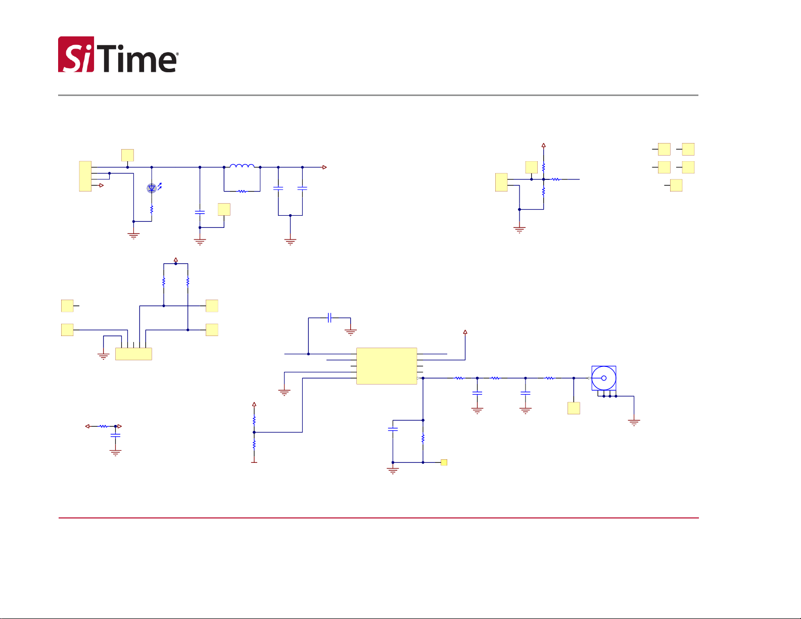
Figure A1 in Appendix A shows the complete electrical schematic of SiT6722EB. Components labeled
“DNP” are not assembled.
Shipment Configuration
SiT6722EB is shipped without components labeled “DNP” on the schematic (see Figure A1 in
Appendix A).
3.1.1 I2C Support
The two pull up resistors (R14 and R15 with 4.7 kΩvalue) can be assembled to support the I2C
configuration (in case I2C master does not have it). If requested, the EVB will ship with these resistors.
3.2 Waveform Capturing Using Active Probe
SiTime Elite Super-TCXO is a high-speed logic output device. It is critical that the proper logic and high
frequency measurement techniques are used along with the high-quality active probe to ensure best
measurement results.
SiTime recommends the following minimum equipment for proper clock waveform measurement
1) 1 GHz bandwidth or higher active probe with capacitance <1 pF, such as an Keysight 1134B
2) Oscilloscope with 4GHz bandwidth or higher such as a Keysight DSA90604A.

SiT6722EB UM Rev 3.0
Page 4 of 8
www.sitime.com
SiT6722EB Evaluation Board User Manual
A passive voltage probe should not be used as it adds a high capacitive load to the part and the long
ground lead clip is not suitable for high frequency measurement applications. The inductance of the long
ground lead coupled with the input capacitance of the probe results in a resonant circuit. The
consequence of this resonance results in the distortion of the clock signal. Typical manifestations of this
distortion include ringing, overshoot, and undershoot of the clock signal.
Eliminating such distortion requires a probe with the lowest input capacitance and a low inductance
ground lead. In addition, SiTime Super-TCXOs are typically configured for fast rise and fall times (1 ns or
less) with 15 pF load. It is therefore critical that the probe tip ground be as short as possible, lowest
inductance, and the return path for the ground be located as close as possible to the trace carrying the
RF logic signal. Please refer to Figure A2 for test point locations on the SiT6722EB and an example of
proper probing.
More details on the SiTime recommendations on the oscillator’s output probing can be found in
AN10028.
3.3 Measuring Jitter and Phase Noise
For jitter measurements, make sure that SMA connector and source termination resistor R11 are
properly soldered on the EVB. R11 value should be 25 Ωfor best source matching (refer to SiTime
AN10002 for more information). The R11 can be populated using one of the following options:
1) 0 Ωresistor. This allows DC coupling the output to 50 Ωinstruments directly. Note that due to
50 Ωloading, the signal swing levels and rise/fall times will be different from those specified
in the datasheet.
2) 0.1 uF capacitor for AC-coupling to 50 Ωinstruments.
SMA connector is used to connect directly to the jitter measurement instrument, such as Time Interval
Analyzer (TIA) or high-bandwidth real-time oscilloscope. Jitter measurement technique is described in
SiTime AN10007.
The SMA can also be connected through 50 Ω coaxial cable to signal source analyzers or spectrum
analyzers to measure phase noise. In such case the use of AC-coupling configuration is recommended
because not all measurement instruments can accept DC voltage at their inputs.
3.4 Current Measurement
To measure the current consumption, user need to use ammeter/multi-meter in the power supply
circuit. We recommend removing diode D1 to avoid measuring the additional current of the diode
circuit. It is recommended to measure the voltage on DUT VDD and adjust for any drop on the DMM to
ensure known VDD voltage on the device. VDD adjustment must be completed before every current
measurement.
Page 5 of 8
www.sitime.com
SiT6722EB Evaluation Board User Manual
Appendix A
Figure A1. SiT6722EB EVB Electrical schematics
"out"
VDD
R3
DNP
R4
DNP
R5
0Pin1
GND
GND
C3
10uF
L1
10uH
R2
10
C1
10uF 0.10uF
GND
VDD
Place away from P1
Place close to DUT VDD pin
C4
NL
Pin1
GND
VDD
GND
GND
Place close to DUT pin1
OUT
Vdd_sense
R16
51k C6
0.10uF
VDD Vdd_sense
GND
1
Pad11
1
Pad2
1
Pad3
1
Pad4
1
Pad5
1
2
3
4
P1
CON/HDR 4pinX1row
GND
R1
50
D1
VAOL-S6GT4 1
2
P2
CON 2pinX1row
OE/VC/NC
1
SCL/NC
2
NC
3
GND
4
A0/NC
5CLK 6
NC 7
NC 8
VDD 9
SDA/NC 10
U1
SiTime_10pin_SE_Ceramic
1
2
3
4
5
P4
CON/HDR 5pinX1row
SDA
A0
SCL
0603
DNP
R8
0603
DNP
R9
GND
VDD
1
Pad7
1
Pad8
1
Pad9
1
Pad10
GND
A0
SDA
SCL
0603
DNP
R14 0603
DNP
R15
VDD
NPO0603
DNP
C5
TP2
GND
0603
DNP
R10
5
1
2
3
4
J1
SMA edge mount
1
Pad12
1
Pad14
1
Pad13
1
Pad15
DNP
R7 DNPR11
DNP
C7
0402
DNP
C8
DNP
R6
GND
GND
GND

SiT6722EB UM Rev 3.0
Page 6 of 8
www.sitime.com
SiT6722EB Evaluation Board User Manual
Table A1. Bill of Materials (BOM)
#
Reference
Designators
Description
Qty
SMD component size
Value
1
C1, C3
Capacitors
2
0603
10uF
2
C2
Capacitor
1
0402
0.1uF
3
C4
Capacitor
1
0402
DNP
4
C5
Capacitor
1
0603
DNP
5
C6
Capacitor
1
0603
0.1uF
6
C7, C8
Capacitor
2
0402
DNP
7
D1
LED
1
0603
Green
8
R1
Resistors
1
0603
50 Ω
9
R2
Resistors
1
0603
10 Ω
10
R3, R4, R8, R9,
R10, R14, R15
Resistor
7
0603
DNP
11
R5
Resistors
1
0603
0 Ω
12
R6, R7, R11
Resistors
3
0402
DNP
13
R16
Resistor
1
0603
51 kΩ
14
L1
Inductor
1
0805
10mH
15
J1
SMA connector
1
-
-
16
P1
4-pin header
1
-
-
17
P2
2-pin header
1
-
-
18
P4
5-pin connector
1
-
-
Table A2. Connectors Digi-Key Part Number
Connectors
Digi-Key
part number
Digi-Key
part number for
mating connector
Digi-Key
part number for
associated products
Power/ Power adjust
WM10159-ND
WM2002-ND
WM1114TR-ND
Pin 1 access
732-5335-ND
WM2011-ND
WM2756CT-ND
Frequency control via I2C
WM4303-ND
WM2014-ND
WM2756CT-ND
OUT
WM5534-ND
23-0732512430-ND
-


SiT6722EB UM Rev 3.0
Page 8 of 8
www.sitime.com
SiT6722EB Evaluation Board User Manual
Table 3: Revision History
Version
Release Date
Change Summary
1.0
30-Mar-2018
Initial Release
2.0
30-Jun-2019
Changed according to next board design
3.0
30-May-2022
Changed according to next board design
SiTime Corporation, 5451 Patrick Henry Drive, Santa Clara, CA 95054, USA | Phone: +1-408-328-4400 | Fax: +1-408-328-4439
© SiTime Corporation, May 2022. The information contained herein is subject to change at any time without notice. SiTime assumes no responsibility or liabi lity for any loss, damage or
defect of a Product which is caused in whole or in part by (i) use of any circuitry other than circuitry embodied in a SiTime product, (ii) misuse or abuse including static discharge, neglect or
accident, (iii) unauthorized modification or repairs which have been soldered or altered during assembly and are not capable of being tested by SiTime under its normal test conditions, or (iv)
improper installation, storage, handling, warehousing or transportation, or (v) being subjected to unusual physical, thermal, or electrical stress.
Disclaimer: SiTime makes no warranty of any kind, express or implied, with regard to this material, and specifically disclaims any and all express or implied warranties, either in fact or by
operation of law, statutory or otherwise, including the implied warranties of merchantability and fitness for use or a particular purpose, and any implied warranty arising from course of dealing or
usage of trade, as well as any common-law duties relating to accuracy or lack of negligence, with respect to this material, any SiTime product and any product documentation. Products sold by
SiTime are not suitable or intended to be used in a life support application or component, to operate nuclear facilities, or in other mission critical applications where human life may be involved
or at stake. All sales are made conditioned upon compliance with the critical uses policy set forth below.
CRITICAL USE EXCLUSION POLICY
BUYER AGREES NOT TO USE SITIME'S PRODUCTS FOR ANY APPLICATION OR IN ANY COMPONENTS USED IN LIFE SUPPORT DEVICES OR TO OPERATE NUCLEAR FACILITIES OR FOR USE IN
OTHER MISSION-CRITICAL APPLICATIONS OR COMPONENTS WHERE HUMAN LIFE OR PROPERTY MAY BE AT STAKE.
SiTime owns all rights, title and interest to the intellectual property related to SiTime's products, including any software, firmware, copyright, patent, or trademark. The sale of SiTime products
does not convey or imply any license under patent or other rights. SiTime retains the copyright and trademark rights in all documents, catalogs and plans supplied pursuant to or ancillary to the
sale of products or services by SiTime. Unless otherwise agreed to in writing by SiTime, any reproduction, modification, translation, compilation, or representation of this material shall be strictly
prohibited.
Table of contents
Other SiTime Motherboard manuals

SiTime
SiTime SiT92216 User manual

SiTime
SiTime SiT6502EB User manual

SiTime
SiTime Time Machine II User manual

SiTime
SiTime SiT6731EB User manual

SiTime
SiTime SiT6098EBB User manual

SiTime
SiTime SiT92113 User manual

SiTime
SiTime SiT6731EB User manual

SiTime
SiTime SiT6098EBB User manual

SiTime
SiTime SiT95314 User manual

SiTime
SiTime Time Machine II User manual


