SiTime SiT6712EB User manual

SiT6712EB UM Rev 1.02
Page 1 of 13
www.sitime.com
SiT6712EB Evaluation Board User Manual
Contents
1 Introduction .............................................................................................................................................1
2 I/O Descriptions .......................................................................................................................................2
3 EVB Usage Descriptions ...........................................................................................................................2
3.1 EVB Configurations........................................................................................................................2
3.1.1 LVPECL, Standard Termination, Active Probe ..................................................................3
3.1.2 LVPECL, AC-coupling Configuration, Direct to Instrument...............................................3
3.1.3 LVPECL, Y-Termination, Active Probe...............................................................................4
3.1.4 LVDS, Standard Termination, Active Probe......................................................................5
3.1.5 LVDS, AC-coupling Configuration, Direct to Instrument ..................................................5
3.1.6 HCSL, Standard Termination, Active Probe......................................................................6
3.1.7 HCSL, Standard Termination, Direct to Instrument .........................................................6
3.2 I2C and SPI Interfaces ....................................................................................................................7
3.3 Waveform Measurement Using Active Probe ..............................................................................7
3.4 Jitter Measurement ......................................................................................................................8
Appendix A –Schematic, BOM and Layout of SiT6712EB.............................................................................9
1Introduction
The SiT6712EB evaluation board (EVB) is designed for use with SiTime’s In-system programmable
oscillators (ISP-DCXO) that support the differential signaling outputs in the 5.0x3.2 mm 10-pin QFN
package. It enables the user to evaluate all aspects of the ISP-DCXO devices including signal integrity,
phase noise, phase jitter and the re-programming of the output frequency via I2C/SPI interfaces.
EVB Features
-Support for SiT3521 (1 to 340 MHz) and SiT3522 (340.000001 to 725 MHz) ISP-DCXOs
-Probing points for output frequency measurements
oSupport for LVPECL, LVDS and HCSL output signal types
oSupport for waveform measurements
oSupport for phase noise and phase jitter measurements
-Connector access to I2C and/or SPI interfaces
-Connector access for current consumption measurements
SiTime typically ships the EVB pre-configured with the ISP-DCXO device specified by the user. The end
user can re-configure the EVB for an ISP-DCXO device of a different configuration.

SiT6712EB UM Rev 1.02
Page 2 of 13
www.sitime.com
SiT6712EB Evaluation Board User Manual
Refer to Section 3for details on EVB configuration and usage.
2I/O Descriptions
Table 1 describes the input/output connectors of the board.
Table 1: SiT6712EB I/O
Designator
I/O
Description
P1
Power
A three-pin connector (P1) for DC power supply to the ISP-DCXO device. Pin’s polarity is identified
on the silkscreen pattern near the connector (see Figure A2). Third pin is used for VDD sensing.
P5
VBIAS
A three-pin connector (P5) intended for supplying bias voltage or supplying negative voltage to
the ISP-DCXO device ground pin for split ground configuration. See Section 3.1 for detailed
information on different termination schemes. Third pin is intended for Vbias sensing.
P1
PIN 1
A three-pin header (P2) provides access to pin 1 of the ISP-DCXO device
P3
PIN 2
A three-pin header (P3) provides access to pin 2 of the ISP-DCXO device
J1/J2
OUT+ and OUT-
OUT+ and OUT- are connected to the frequency output of the ISP-DCXO device. The output should
be measured using either the hi-impedance, hi-bandwidth active probe or via the SMA connectors
(J1 and J2). Section 3.1 describes in detail the recommended measurement configurations.
P4
Current
Measurement
A two-pin connector (P4) enables the current consumption measurement of the ISP-DCXO device.
To measure the current, remove zero-ohm resistors R1 and R19, and connect the DMM or other
current measuring device across this connector. It is recommended to measure the voltage on
VDD pin and adjust for any drop on the DMM to ensure known VDD voltage on the device.
P6
Frequency
control via
I2C/SPI
A five-pin header (P6) provides access to I2C (SDA, SCL) or SPI (MOSI, MISO, SCL) of the ISP-DCXO
device.
Note: Pin 1 location of the ISP-DCXO device on EVB is indicated by a chamfer in the silkscreen pattern
around the device footprint.
3EVB Usage Descriptions
3.1 EVB Configurations
The SiT6712EB supports multiple configurations for different signaling types of SiTime differential
oscillators by using different component loading options.
Refer to
-Figure A1 in Appendix A for the SiT6712EB schematics
-Figure A2 in Appendix A for the SiT6712EB layout top view
SiT6712EB UM Rev 1.02
Page 3 of 13
www.sitime.com
SiT6712EB Evaluation Board User Manual
Note that not all components shown in the schematics are populated for all configurations of the EVB.
Specifically,
-Any components with assigned nominal values are used in all configurations of the EVB
-Any components without assigned nominal values are populated only for specific configuration
of EVB where these parts are needed
-Any components labeled “DNP” are not populated on the EVB and are reserved for SiTime internal
use only
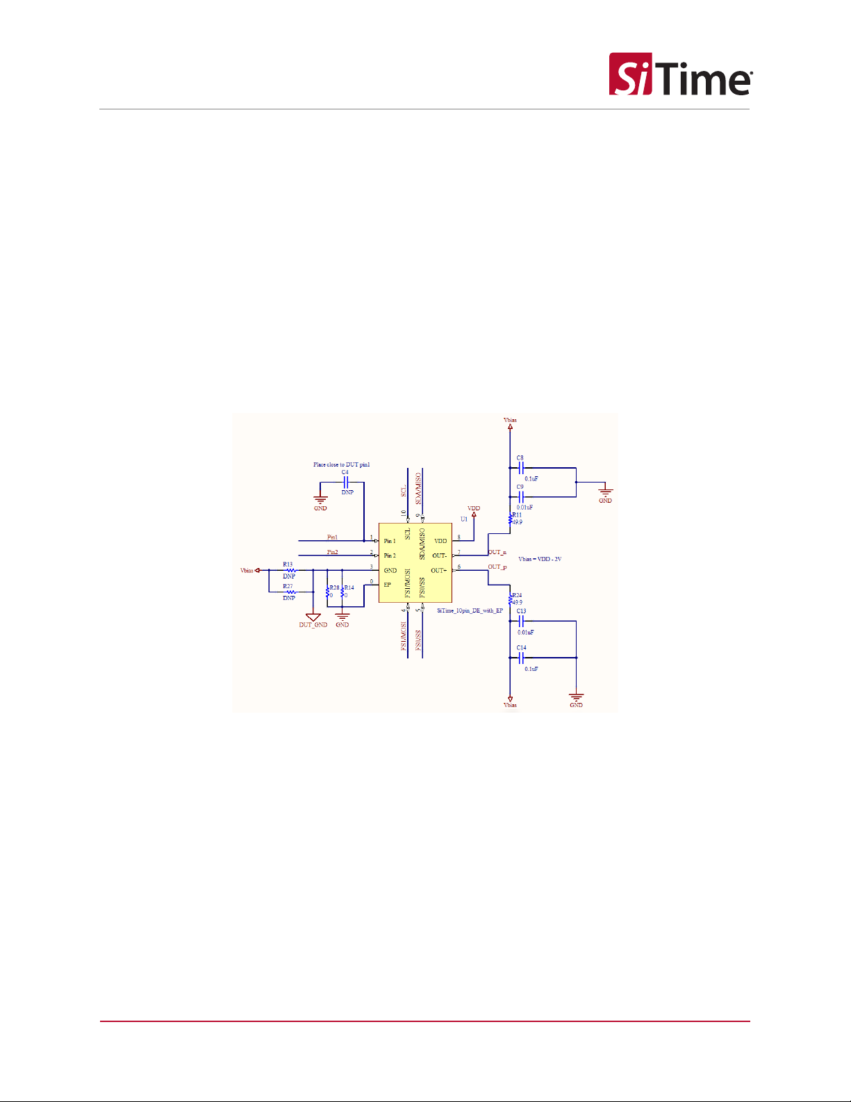
3.1.1 LVPECL, Standard Termination, Active Probe
In this configuration, the LVPECL outputs are terminated to Vbias = VDD –2 V with 50 Ω resistors (R11
and R24). A high-speed active probe, as shown on Figure 1, is placed on the termination resistor’s pads
which are on the OUT+ and OUT- traces. Figure 1 shows the termination scheme for this configuration.
Figure 1: LVPECL output termination with 50 Ω to Vbias and measurement
using high impedance and high bandwidth active probe
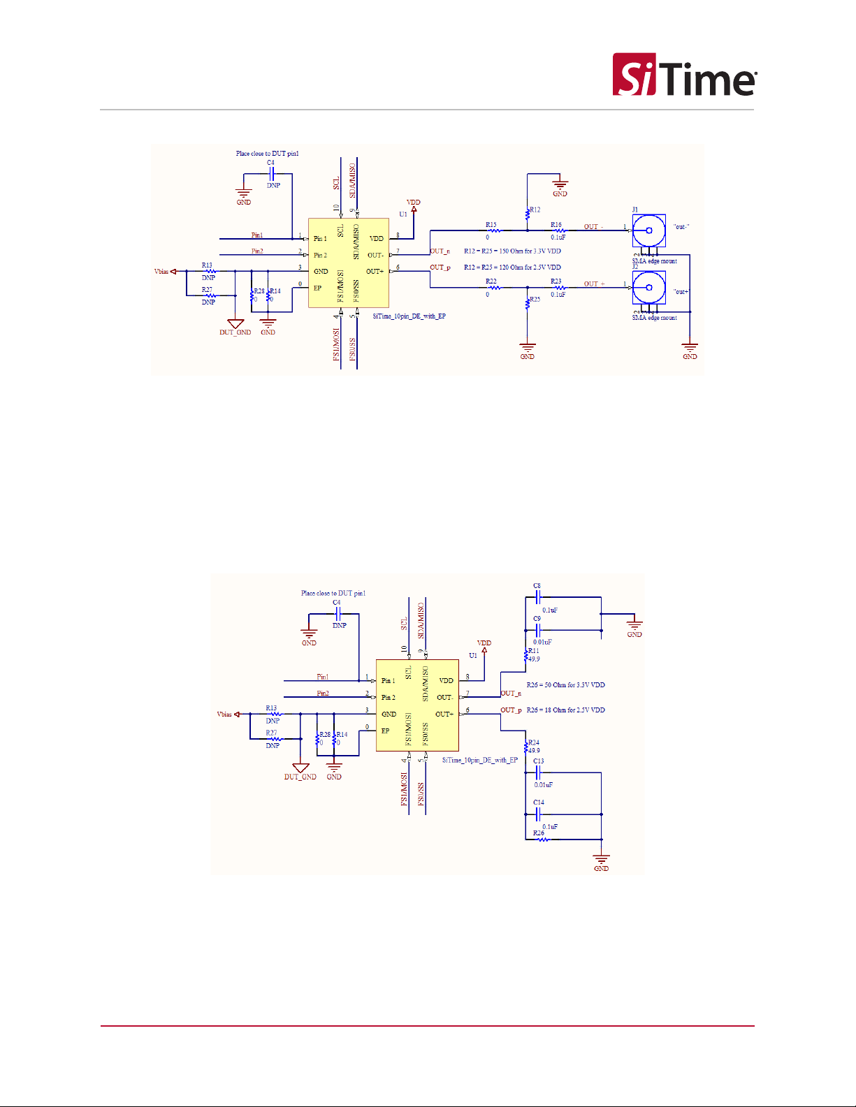
3.1.2 LVPECL, AC-coupling Configuration, Direct to Instrument
This is default shipment configuration for evaluation boards with LVPECL devices.
This configuration allows LVPECL output connection to the measurement instrument using 50 Ω coaxial
cables. Outputs are terminated with 150 Ω/120 Ω (R15 and R22; for 3.3 V and 2.5 V VDD respectively) to
GND on the DUT side and connected to SMA connectors through 0.1 uF series capacitors (R16 and R23).
Figure 2 shows the termination scheme for this configuration.
SiT6712EB UM Rev 1.02
Page 4 of 13
www.sitime.com
SiT6712EB Evaluation Board User Manual
Figure 2: LVPECL output termination with 150 Ω/120 Ω to GND and measurement with
AC-coupled connection to measurement instrument using 50 Ω SMA cables
3.1.3 LVPECL, Y-Termination, Active Probe
This configuration is intended for LVPECL output waveform parameters measurement using active
probe.
Figure 3 shows termination scheme for this configuration. R26 is added to create DC voltage bias for
OUT+ and OUT- with R24 (50 Ω) and R11 (50 Ω). R26 is 50 Ω for 3.3 V VDD and 18 Ω for 2.5 V VDD.
Figure 3: Y-termination scheme for LVPECL output termination for measurement
using high impedance and high bandwidth active probe
SiT6712EB UM Rev 1.02
Page 5 of 13
www.sitime.com
SiT6712EB Evaluation Board User Manual
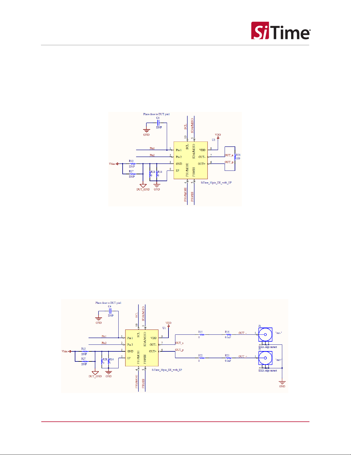
3.1.4 LVDS, Standard Termination, Active Probe
This configuration is intended for LVDS output waveform parameters measurement using active
probe. A high-speed active probe, as shown on Figure 4 is placed on the termination resistor’s pads which
are on the OUT+ and OUT- traces.
Figure 4 shows differential impedance of 100 Ω (R21) across OUT+ and OUT- for termination.
Figure 4: 100 Ω differential impedance across LVDS outputs for measurement using
high impedance and high bandwidth active probe
3.1.5 LVDS, AC-coupling Configuration, Direct to Instrument
This is default shipment configuration for evaluation boards with LVDS devices.
This configuration is useful for connecting LVDS outputs to 50 Ω input channels of the measurement
instrument. The AC-coupling capacitors (R16 and R23) block the DC common mode voltage from the
LVDS outputs to avoid DC current draw to the 50 Ω inputs. Figure 5 shows termination scheme for this
configuration.
Figure 5: AC-coupled LVDS outputs are terminated by measurement instrument input 50 Ω
impedance, equivalent 100 Ω across OUT+ and OUT-
SiT6712EB UM Rev 1.02
Page 6 of 13
www.sitime.com
SiT6712EB Evaluation Board User Manual
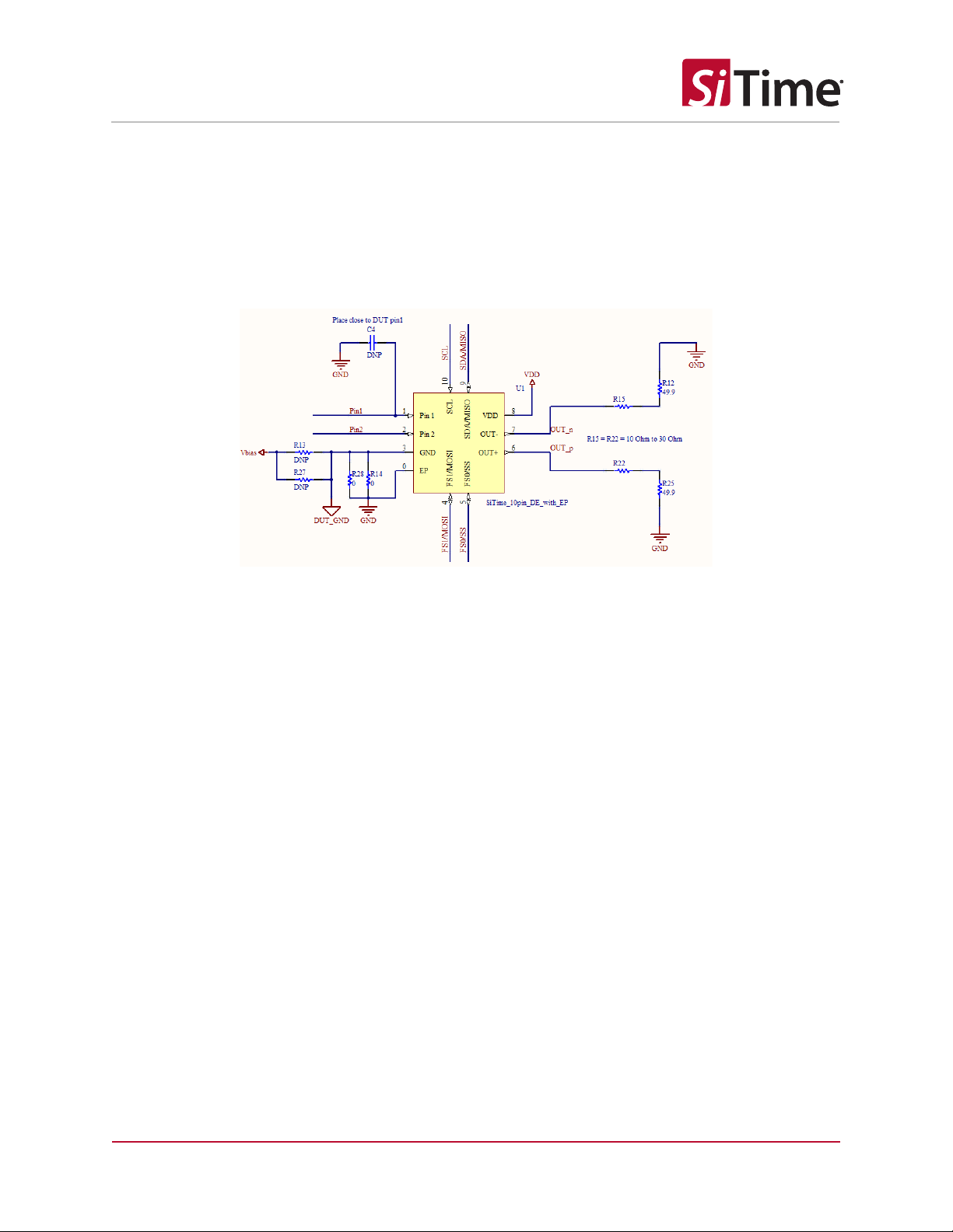
3.1.6 HCSL, Standard Termination, Active Probe
This configuration is intended for HCSL output waveform parameters measurement using active probe.
Output is terminated with 50 Ω (R12 and R25) to GND. Series resistors R15 and R22 are used as
overshoot limiter and should be in range from 10 Ωto 30 Ω. A high speed active probe is placed on the
termination resistor’s pads which are on the OUT+ and OUT- traces. Figure 6 shows termination scheme
for this configuration.
Figure 6: HCSL outputs terminated with 50 Ω to GND through 10 Ω to 30 Ω series resistors for
measurement using high impedance and high bandwidth active probe
3.1.7 HCSL, Standard Termination, Direct to Instrument
This is default shipment configuration for evaluation boards with HCSL devices.
This configuration is intended for HCSL output waveform parameters measurement with direct
connection to measurement instrument 50 Ω inputs.
Figure 7 shows termination scheme for this configuration. Series resistors R15 and R22 are used as
overshoot limiter and should be in range of 10 Ω to 30 Ω.
SiT6712EB UM Rev 1.02
Page 7 of 13
www.sitime.com
SiT6712EB Evaluation Board User Manual
Figure 7: HCSL outputs terminated with 50 Ω to GND at measurement instrument side with 10 Ω to 30
Ω series resistors at source side
3.2 I2C and SPI Interfaces
Both I2C and SPI interfaces are supported via the P6 5-pin connector. Two pull up resistors –R20 (4.7 kΩ)
and R30 (4.7 kΩ) – must be populated for the I2C support. SPI interface doesn’t require these two
resistors. The EVB ships preconfigured for either the I2C or the SPI support per user specification.
3.3 Waveform Measurement Using Active Probe
SiTime differential oscillators are high speed logic output devices with fast, sub-nanosecond rise/fall
time. It is critical that the proper logic and high frequency measurement techniques are used along with
the high-quality active probe to ensure best measurement results.
SiTime recommends the following equipment for proper measurement of a differential clock waveform:
1) Differential active probe with >4GHz bandwidth, <1pF load capacitance, such as an
Agilent 1134A, with high-speed differential probe heads, such as:
a. Agilent E2675B differential browser
b. Agilent N5381B solder-down probe tip
c. Agilent N5425B/N5426A ZIF probe tip
2) Oscilloscope with 4 GHz bandwidth or higher
3) Oscilloscope with 50 Ω inputs.
Please refer to Figure 8 for a probing example on the EVB using active probe.

SiT6712EB UM Rev 1.02
Page 8 of 13
www.sitime.com
SiT6712EB Evaluation Board User Manual
Figure 8: Differential browser (high impedance active probe) on test points for
waveform capturing on the SiT6712EB EVB
3.4 Jitter Measurement
For jitter measurement, configurations described in 3.1.1 (LVPECL), 3.1.4 (LVDS) and 3.1.6 (HCSL) should
be used. Jitter measurement technique is described in SiTime application note AN10007.

SiT6712EB UM Rev 1.02
Page 9 of 13
www.sitime.com
SiT6712EB Evaluation Board User Manual
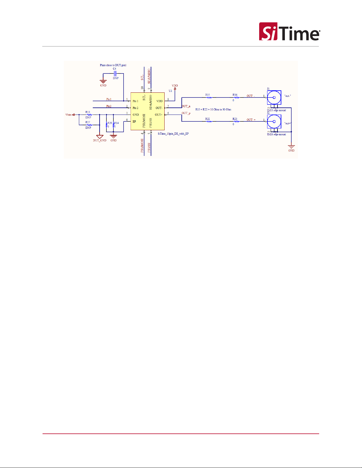
Appendix A –Schematic, BOM and Layout of SiT6712EB
Figure A1: SiT6712EB rev. 2.01 schematic
"curr_meas_inp"
"curr_meas_out"
"out-"
"out+"
1
2
3
P5
GND
C5
10uF
L2
10uH
R9
10
C6
0.1uF
C7
0.01uF
Vbias
1
2
3
P2
VDD
R3
NL
R7
NL
R5
51
R4
NL
R8
NL
R6
51
Pin1
GND
VDD
GND
Pin2
GND
R1
0
C3
10uF
L1
10uH
R2
10
C1
10uF
C2
0.1uF
DUT_GND
GND
VDD
Place away from P1 and P4
Place close to DUT VDD pin
C4
NL
R13
NL
R14
0
Pin1
GND
DUT_GND
Pin2
VDD
R21
TBD
R11
TBD
R24
TBD
R15
TBD
R22
TBD
R12
TBD
R25
TBD
R16
TBD
R23
TBD
1
2
3
4
J1
1
2
3
4
J2
GND
OUT_p
OUT_n
GND
GND
R10
TBD
R26
TBD
C8
0.1uF
C9
0.01uF
C13
0.01uF
C14
0.1uF
GND
Place close to DUT pin1
Vbias_sense
1
2
3
P3
1
2
P4
OUT_-
OUT_+
R29
51k
C15
0.10uF
Vbias
Vbias_sense
GND
R27
NL
R28
0
1
2
3
P1
Vdd_sense
R31
51k
C17
0.10uF
VDD
Vdd_sense
GND
Vbias
Vbias
Vbias
DUT_GND
DUT_GND
R17
NL
R18
NL
Vbias
VDD
R19
0
FS1/MOSI
FS0/SS
SDA/MISO
SCL
GND
GND
30
R34
4.7K
R20
4.7K
R30
SDA/MISO
SCL
VDD
1
2
3
4
5
P6
R32
NL
R35
NL
DUT_GND
FS1/MOSI
FS0/SS
R33
NL
R36
NL
GND
Pin 1
1
Pin 2
2
OUT-
7
GND
3
OUT+
6
VDD
8
SCL
10
SDA/MISO
9
FS1/MOSI
4
FS0/SS
5
EP
0
U1
SiTime Device
C10
NL
C11
NL

SiT6712EB UM Rev 1.02
Page 10 of 13
www.sitime.com
SiT6712EB Evaluation Board User Manual
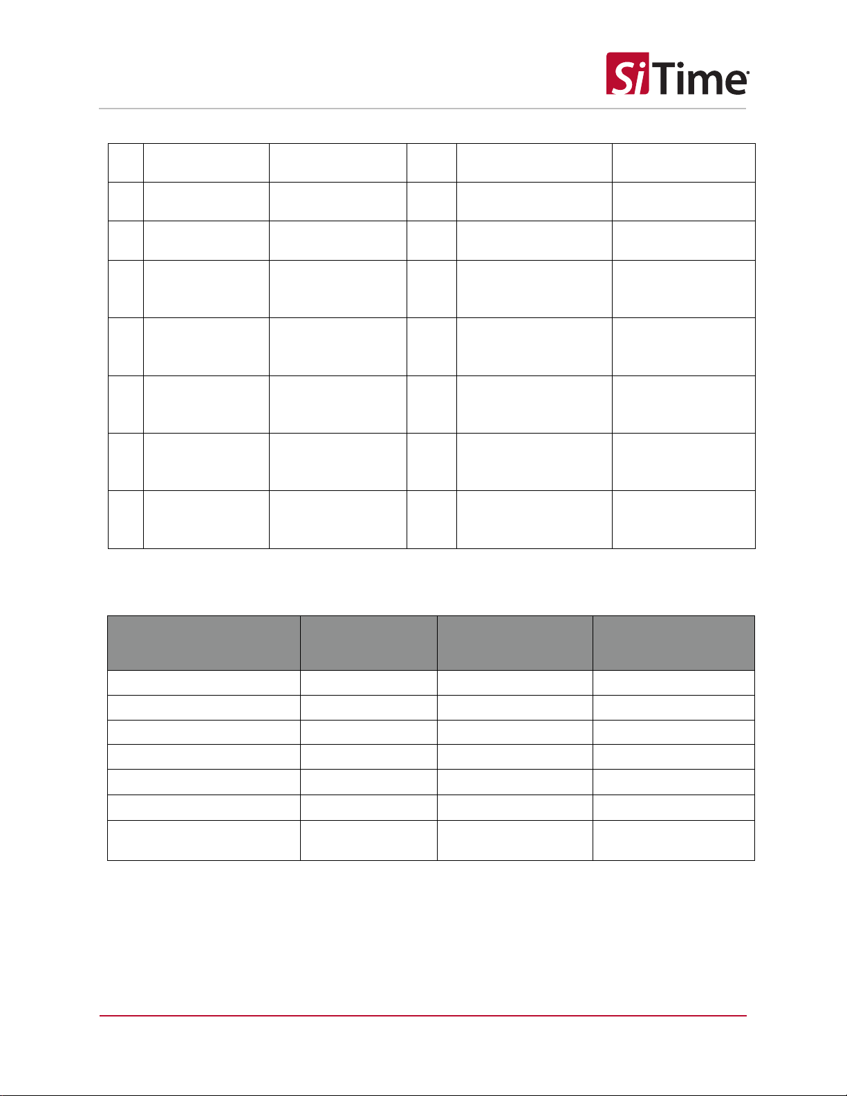
Table A1: Bill of Materials (BOM)
#
Reference
Designators
Description
Qty
SMD component size
Value
1
R1, R19
Resistor
2
0603
0 Ω
2
R14, R28
Resistor
2
0402
0 Ω
3
R2, R9,
Resistor
2
0603
10 Ω
4
R5, R6
Resistor
2
0603
51 Ω
5
R29, R31
Resistor
2
0603
51 kΩ
6
R20, R30
Resistor
2
0603
4.7 kΩ
7
R3, R4, R7, R8,
R32, R33, R35,
R36
Resistor
8
0603
Don’t populated
8
R13, R27, R17,
R18
Resistor
4
0402
Don’t populated
9
R21
Resistor
1
0603
See Figure 1~8
for values
10
R10, R11, R12,
R15, R16, R22,
R23, R24, R25,
R26
Resistor
10
0402
See Figure 1~8
for values
11
L1, L2
Inductor
2
0805
10 uH
12
C1, C3, C5
Ceramic capacitor
3
0603
10 uF
13
C2
Ceramic capacitor
1
0402
0.1 uF
14
C6, C8, C14, C15,
C17
Ceramic capacitor
5
0603
0.1 uF
15
C7, C9, C13
Ceramic capacitor
4
0402
0.01 uF
SiT6712EB UM Rev 1.02
Page 11 of 13
www.sitime.com
SiT6712EB Evaluation Board User Manual
16
C4
Ceramic capacitor
1
0603
Don’t populated
17
C10, C11
Ceramic capacitor
2
0402
Don’t populated
18
U1
SiTime Oscillator
1
19
P1, P5
3-pin connector
2
Through hole, 2.54
mm pitch
20
P2, P3
3-pin header
2
Through hole, 2.54
mm pitch
21
P6
5-pin header
1
Through hole, 2.54
mm pitch
22
P4
2-pin connector
1
Through hole, 2.54
mm pitch
23
J1, J2
SMA connectors
2
See Figure 1~8
for values
Table A2: Connectors Digi-Key Part Number
Connectors
Digi-Key
part number
Digi-Key
part number for mating
connector
Digi-Key
part number for
associated products
Power
WM2701-ND
WM2001-ND
WM1114-ND
Vbias
WM2701-ND
WM2001-ND
WM1114-ND
Pin 1
609-3461-ND
76341-303LF-ND
Pin 2
609-3461-ND
76341-303LF-ND
Frequency control via I2C/SPI
609-3462-ND
76341-305LF-ND
Output
WM5534-ND
Power Supply Current
Measurement
WM2744-ND
WM2011-ND
WM1114-ND

SiT6712EB UM Rev 1.02
Page 13 of 13
www.sitime.com
SiT6712EB Evaluation Board User Manual
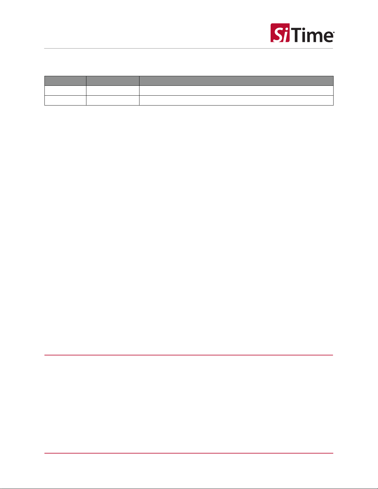
Table 2: Revision History
Version
Release Date
Change Summary
1.01
24-Oct-2017
Initial Release
1.02
20-Jan-2023
Updated Appendix A for 2.01 board revision design.
SiTime Corporation, 5451 Patrick Henry Drive, Santa Clara, CA 95054, USA | Phone: +1-408-328-4400 | Fax: +1-408-328-4439
© SiTime Corporation, January 2023. The information contained herein is subject to change at any time without notice. SiTime assumes no responsibility or liability for any loss, damage
or defect of a Product which is caused in whole or in part by (i) use of any circuitry other than circuitry embodied in a SiTime product, (ii) misuse or abuse including static discharge, neglect or
accident, (iii) unauthorized modification or repairs which have been soldered or altered during assembly and are not capable of being tested by SiTime under its normal test conditions, or (iv)
improper installation, storage, handling, warehousing or transportation, or (v) being subjected to unusual physical, thermal, or electrical stress.
Disclaimer: SiTime makes no warranty of any kind, express or implied, with regard to this material, and specifically disclaims any and all express or implied warranties, either in fact or by
operation of law, statutory or otherwise, including the implied warranties of merchantability and fitness for use or a particular purpose, and any implied warranty arising from course of dealing or
usage of trade, as well as any common-law duties relating to accuracy or lack of negligence, with respect to this material, any SiTime product and any product documentation. Products sold by
SiTime are not suitable or intended to be used in a life support application or component, to operate nuclear facilities, or in other mission critical applications where human life may be involved
or at stake. All sales are made conditioned upon compliance with the critical uses policy set forth below.
CRITICAL USE EXCLUSION POLICY
BUYER AGREES NOT TO USE SITIME'S PRODUCTS FOR ANY APPLICATION OR IN ANY COMPONENTS USED IN LIFE SUPPORT DEVICES OR TO OPERATE NUCLEAR FACILITIES OR FOR USE IN
OTHER MISSION-CRITICAL APPLICATIONS OR COMPONENTS WHERE HUMAN LIFE OR PROPERTY MAY BE AT STAKE.
SiTime owns all rights, title and interest to the intellectual property related to SiTime's products, including any software, firmware, copyright, patent, or trademark. The sale of SiTime products
does not convey or imply any license under patent or other rights. SiTime retains the copyright and trademark rights in all documents, catalogs and plans supplied pursuant to or ancillary to the
sale of products or services by SiTime. Unless otherwise agreed to in writing by SiTime, any reproduction, modification, translation, compilation, or representation of this material shall be strictly
prohibited.
Table of contents
Other SiTime Motherboard manuals

SiTime
SiTime SiT6760EB User manual

SiTime
SiTime SiT6731EB User manual

SiTime
SiTime Time Machine II User manual

SiTime
SiTime SiT95314 User manual

SiTime
SiTime SiT6503EB User manual

SiTime
SiTime SiT92216 User manual

SiTime
SiTime SiT92113 User manual

SiTime
SiTime SiT6731EB User manual

SiTime
SiTime SiT6098EBB User manual

SiTime
SiTime SiT6722EB User manual


