SiTime SiT92113 User manual

SiT92113EB User Manual | Rev 0.5
Page 1 of 24
www.sitime.com
SiT92113 Ultra Low Jitter Buffer Evaluation Kit User Guide
Table of Contents
1Introduction ......................................................................................................................................................................... 2
2Features.............................................................................................................................................................................. 2
3Functional Description......................................................................................................................................................... 3
3.1. VDD and VDDO Power Supplies.............................................................................................................................3
3.2. Clock Inputs.............................................................................................................................................................3
3.3. Clock States (Input vs Output States)......................................................................................................................3
3.4. Output Enable..........................................................................................................................................................4
4Power Supply Connections................................................................................................................................................. 4
5Setting Input Clock Select and Output Enable in the EVB................................................................................................... 6
6Input Clock Configuration.................................................................................................................................................... 7
7Configuring for Single ended AC coupled Input Clock ........................................................................................................ 8
7.1. Driving Clock Inputs with LVCMOS Driver (AC coupled).........................................................................................8
8Configuring EVB for DC Coupled Input LVCMOS Clock..................................................................................................... 9
8.1. Driving Clock Inputs with LVCMOS Driver (DC coupled).........................................................................................9
8.2. EVB Changes for Driving Clock Inputs with LVCMOS Driver (DC coupled, single ended)......................................9
9Driving Differential LVDS or LVDS Boost (AC coupled).................................................................................................... 11
10 Board Configuration for driving DC Coupled LVDS........................................................................................................... 12
10.1.LVDS (DC coupled) ............................................................................................................................................... 12
10.2.Board Changes Required for DC Coupled LVDS ..................................................................................................12
11 Board Configuration Required for Driving DC/AC coupled LVPECL ................................................................................. 13
11.1.DC/AC Coupled LVPECL.......................................................................................................................................13
12 EVB Snapshot................................................................................................................................................................... 14
13 PCB Schematic................................................................................................................................................................. 15
13.1.Schematic Sheet 1................................................................................................................................................. 15
13.2.Schematic Sheet 2................................................................................................................................................. 16
13.3.Schematic Sheet 3................................................................................................................................................. 17
13.4.Schematic Sheet 4................................................................................................................................................. 18
13.5.Schematic Sheet 5................................................................................................................................................. 19
13.6.Schematic Sheet 6................................................................................................................................................. 20
13.7.Schematic Sheet 7................................................................................................................................................. 21
13.8.Schematic Sheet 8................................................................................................................................................. 22
SiT92113 Ultra Low Jitter Buffer Evaluation Kit User Guide
SiT92113EB User Manual | Rev 0.5
Page 2 of 24
www.sitime.com
1 Introduction
The SiT92113 Evaluation Board is designed for evaluating the SiT92113, 5 output low-jitter clock, fan-out buffer, intended to
be used in low jitter, high frequency clock/data distribution and level translation.
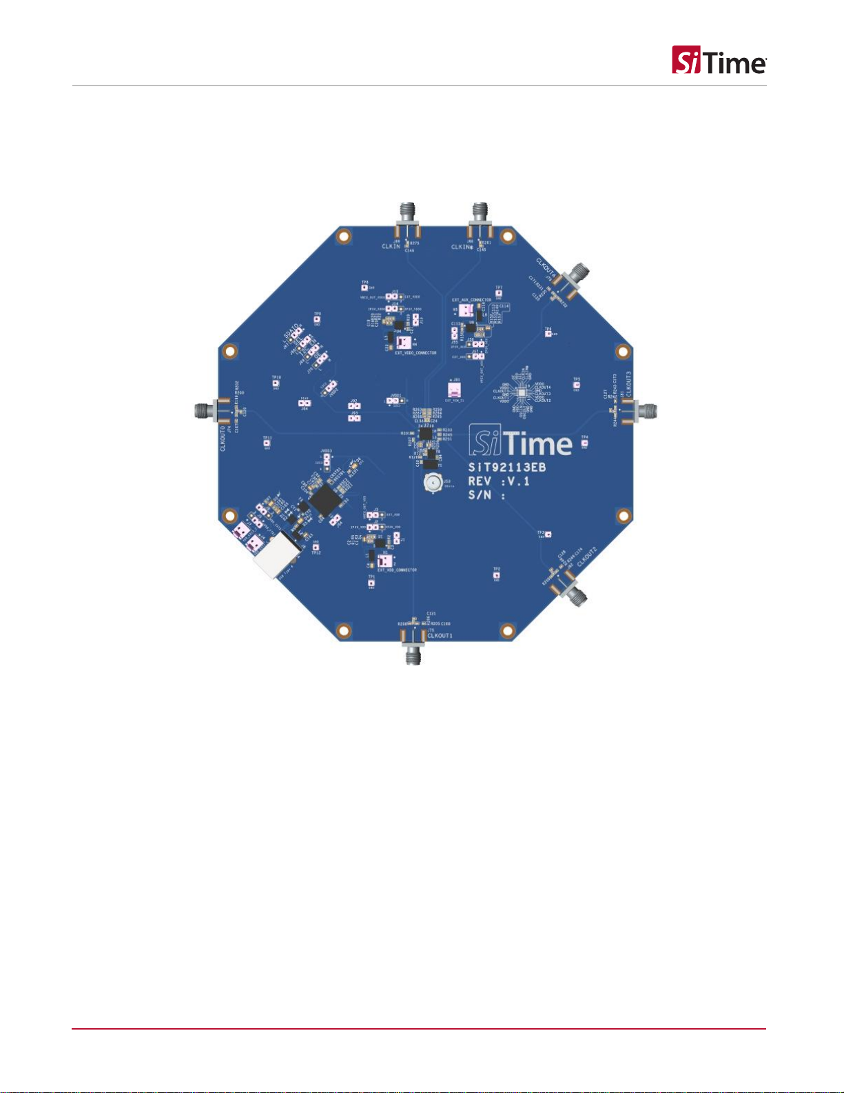
Figure 1. SiT92113 EVB Board
2 Features
1) Additive jitter performance of 50 fs RMS.
2) Typical output skew between clock outputs is 30 ps.
3) Level translation with core supply voltage of 3.3 V/2.5 V/1.8 V and 3.3 V/2.5 V/1.8 V/1.5 V output supply for
LVCMOS output drivers.
4) The device inputs consist of 1 differential and crystal inputs.
5) The inputs are selected by programming input select pins of SIT92113. The input clock receiver in SiT92113 can
accept LVPECL, LVDS, LVCMOS, SSTL, HCSL and XTAL waveforms.
6) Crystal frequencies from 8 MHz to 50 MHz are supported.
7) Crystal input can be over driven with frequency up to 250 MHz in crystal bypass mode.
SiT92113 Ultra Low Jitter Buffer Evaluation Kit User Guide
SiT92113EB User Manual | Rev 0.5
Page 3 of 24
www.sitime.com
3 Functional Description
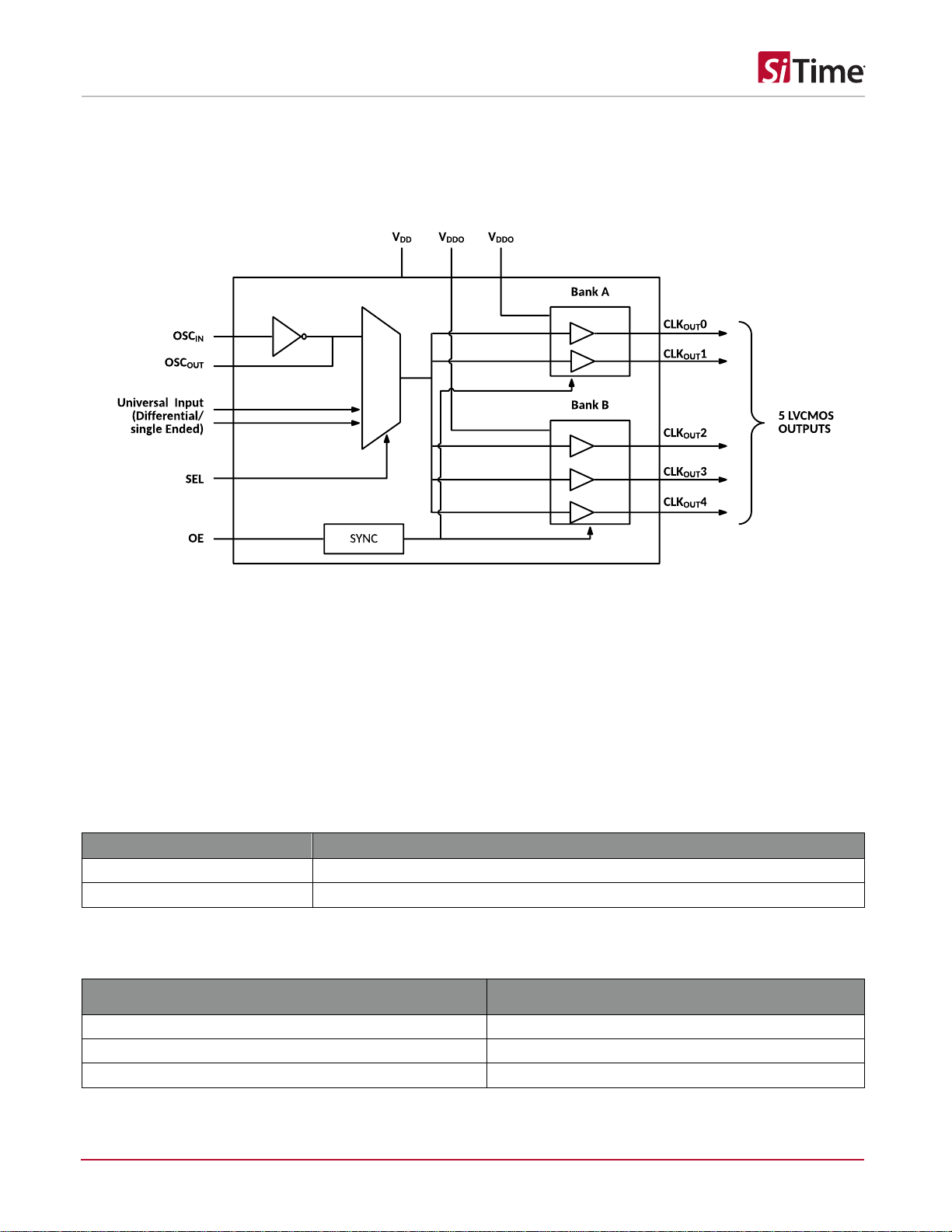
The SiT92113 is a 5-output single ended clock fan out buffer with low additive jitter that can operate up to 250MHz. It features
a 2:1 input multiplexer with an optional crystal oscillator input and five LVCMOS output. The input selection and output buffer
modes are controlled via pin strapping. The device is offered in a 24-pin QFN package.
Figure 2. Functional Diagram
3.1. VDDand VDDOPower Supplies
The SiT92113 has separate 3.3/2.5/1.8 V core (VDD) and 3.3/2.5/1.8/1.5 V output power supply (VDDO). Output supply
operation at 2.5/1.8/1.5 V enables lower power consumption and output-level compatibility with 2.5/1.8/1.5 V receiver devices.
The output levels LVCMOS (VOH) is referenced to its respective VDDO supply.
3.2. Clock Inputs
The input clock can be selected from clock input or OSCIN. Clock input selection is controlled using the SEL input as shown in
Table 1.
Table 1. Input Clock Selection
SEL
Selected Clock
0
CLK0
1
Crystal Or Crystal bypass AC coupled mode
3.3. Clock States (Input vs Output States)
Table 2. Input versus Output Stages
State of Selected Clock input
Output State
Inputs are floating
Logic low
Inputs are logic low
logic low
Inputs are logic high
logic high
SiT92113 Ultra Low Jitter Buffer Evaluation Kit User Guide
SiT92113EB User Manual | Rev 0.5
Page 4 of 24
www.sitime.com
3.4. Output Enable
Pulling OE to LOW, forces the outputs to the high-impedance state after the next falling edge of the input signal. The outputs
remain in the high-impedance state as long as OE is LOW. The OE signal is internally synchronized to the selected input
clock. This allows disabling the output clock at the falling edge of input clock in a glitch free manner.
Table 3. OE Functionality
OE
Output State
0
Disabled (HiZ)
1
Enabled
4 Power Supply Connections
SiT92113 buffer has two supplies VDD and VDDO. The VDDO supply is dedicated supply for the output LVCMOS drivers. The
VDDO supply can be 3.3 V+/-5 %, 2.5 V+/-5 %, 1.8 V+/-10 %, 1.5 V+/-10 %. The VDD supply is dedicated for the input clock
receiver, clock distribution unit and the XO inside SIT92113. This supply is independent of VDDO. The VDD supply can vary
from 3.3 V+/-5%, 2.5 V+/-5%, and 1.8 V +/- 5%.
The VDD, VDDO supplies can be set as per Table 4.
Table 4 Power supply connections for SiT92113 EVB
Power Source
Jumper setting
Comments
PC/Laptop USB port
J5 shorted between pins 1,2
Default EVB configuration
Single External Source of 5V
J5 shorted between pins 2,3
Connect the USB cable from PC/laptop USB port to the USB receptacle of the EVB
after connecting the USB. SiT92113 will power up with VDD=VDDO = 3.3 .
to different voltage levels using jumper settings as shown in Table 5.
Table 5. Setting VDD supply voltage
LDO
Jumper setting
VDD (V)
U1
J2 shorted between pins 2,3
3.3
J2 shorted between pins 1,2
2.5
J2 left open
1.8
Note:
1. Refer Figure 11. Schematic Sheet 1 VDD (Input Side Supply) for Jumper J2 connection.
2. VDD output is set to 3.3 V using U1 LDO in the EVB
Table 6. Setting VDDO voltage
LDO
Jumper setting
VDDO (V)
U4
J14 shorted between pins 2,3
3.3
J14 shorted between pins 1,2
2.5
J14 left open
1.8
Note:
1. Refer for Figure 12. Schematic Sheet 2 VDDO (Output Side Supply) Jumper J14 connection.
2. VDDO output is set to 3.3V using U4 LDO in the EVB
3. LDO feedback resistors are selected to support 3.3, 2.5and 1.8V operation on VDDO.

SiT92113 Ultra Low Jitter Buffer Evaluation Kit User Guide
SiT92113EB User Manual | Rev 0.5
Page 5 of 24
www.sitime.com
Table 7. Setting VDD_AUX voltage
LDO
Jumper setting
VDD_AUX (V)
U8
J56 shorted between pins 2,3
3.3
J56 shorted between pins 1,2
2.5
J56 left open
1.8
Note:
1. Refer Figure 13. Schematic Sheet 3 Auxiliary Supply for Jumper J56 connection.
2. VDD_AUX is the supply of level shifter outputs for automated control of input clock select, output enable.
3. Keep VDD = VDD_AUX
4. VDD_AUX is set to 3.3V using U8 LDO in the EVB

SiT92113 Ultra Low Jitter Buffer Evaluation Kit User Guide
SiT92113EB User Manual | Rev 0.5
Page 6 of 24
www.sitime.com
5 Setting Input Clock Select and Output Enable in the EVB
The jumper setting for controlling the input clock select and output enable are given in Table 8.
Table 8. Jumper settings to control clock select and output enable
Pin
Jumper state
Logic state
SEL
J68 shorted between 2,3
XO
J68 shorted between 1,2
CLKIN 0
OE
J70 shorted between 2,3
0
J70 shorted between 1,2
1
Note:
1. The programming for input clock select is given below. Input clock select programming: 1'b0 - clock0, 1'b1 - XO
2. Refer Figure 16. Schematic Sheet 6 FTDI to DUT Mapping for Jumper J68, J67 connection.
3. The programming for OE is given below. OE programming: 1'b0 - output disable, 1'b1 - output enable
4. Refer Figure 16. Schematic Sheet 6 FTDI to DUT Mapping for Jumper J70 connection.
5. J69 should always remain in its default state: between pin2 and pin3.
6. Jumpers labelled as JVDD1, JVDD2, JVDD3, Diag should be left in their default state: floating.
7.

SiT92113 Ultra Low Jitter Buffer Evaluation Kit User Guide
SiT92113EB User Manual | Rev 0.5
Page 7 of 24
www.sitime.com
6 Input Clock Configuration
The input clock is ac coupled and terminated with differential 100 EVB is configured for differential input clock as
shown in Figure 17.
Figure 3. Input Clock Configuration
SiT92113 Ultra Low Jitter Buffer Evaluation Kit User Guide
SiT92113EB User Manual | Rev 0.5
Page 8 of 24
www.sitime.com
7 Configuring for Single ended AC coupled Input Clock
Many applications require the buffer to receive single ended input clock. Therefore, some minimal changes need to be done to
the EVB to accomplish single ended operation.
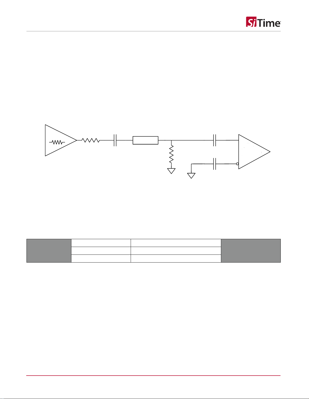
7.1. Driving Clock Inputs with LVCMOS Driver (AC coupled)
For large single-ended input signals, such as 3.3 V or 2.5 V LVCMOS, a 50 load resistor should be placed near the input for
signal attenuation to prevent input overdrive as well as for line termination to minimize reflections. The single-ended input slew
rate should be as high as possible to minimize performance degradation. The clock input has an internal bias voltage of about
(VDD-0.3)/2 V, so the input can be AC coupled as shown in Figure 4.The output impedance of the LVCMOS driver plus Rs
should be close to 50 to match the characteristic impedance of the transmission line and load termination.
Figure 4. Single ended LVCMOS input, AC coupling
EVB Changes for Driving Clock Inputs with LVCMOS Driver (AC coupled, single ended)
The board changes are listed in the Table 9:
Table 9. Board component changes required to support single ended AC coupled LVCMOS
Clock 0 path
R275
change to 0.1uF
Schematic Sheet 2
C156
change to 0 Ohms
R259
change to 0 Ohms

SiT92113 Ultra Low Jitter Buffer Evaluation Kit User Guide
SiT92113EB User Manual | Rev 0.5
Page 9 of 24
www.sitime.com
8 Configuring EVB for DC Coupled Input LVCMOS Clock
8.1. Driving Clock Inputs with LVCMOS Driver (DC coupled)
Single ended clocks can be DC coupled to the SiT92113 Buffer. If the CLK0 is driven, nCLK0 voltage must be set using a
resistor divider to match the common mode of the DC coupled single ended clock.
This is shown Figure 5.
Figure 5. DC coupled single ended CMOS input clock
8.2. EVB Changes for Driving Clock Inputs with LVCMOS Driver (DC coupled, single
ended)
Case1:
SIT92113. Let the supply of LVCMOS driver be 1.8 V. Then the swing of the clock at the chip input is 0.9 Vpp. We to set the
reference voltage at the reference node at 0.45 V. Choose VCC = 1.8 V, Rs2 = 3Rs1. Rs1 and Rs2 should be in the kilo ohm
range. So, if we set Rs1 = 3K, Rs2 = 1 K.
Table 10. EVB board changes required to support single ended DC coupled LVCMOS
Clock 0 path
R259
Remove
Schematic Sheet 2
C24
change to 0 Ohms
R264
change to 3KOhms
R265
change to 1k Ohms
C145
populate with 0.1uF
C154
change to 0 Ohms
C156
change to 0 Ohms

SiT92113 Ultra Low Jitter Buffer Evaluation Kit User Guide
SiT92113EB User Manual | Rev 0.5
Page 10 of 24
www.sitime.com
Case2: if load is purely capacitive, then we just need to float the reference node with 0.1 uF capacitor attached to it. The
reference node is biased internally to VCC/2.
Figure 6. Single ended LVCMOS input, DC coupling Capacitive load
Table 11. Single ended DC coupling for driving pure capacitive load
Clock 0 path
R259
Remove
Schematic Sheet 2
R263
remove
C24
change to 0 Ohms
R264
change to 1K Ohms
R265
change to 1K Ohms
C145
populate with 0.1uF
C154
change to 0 Ohms
SiT92113 Ultra Low Jitter Buffer Evaluation Kit User Guide
SiT92113EB User Manual | Rev 0.5
Page 11 of 24
www.sitime.com
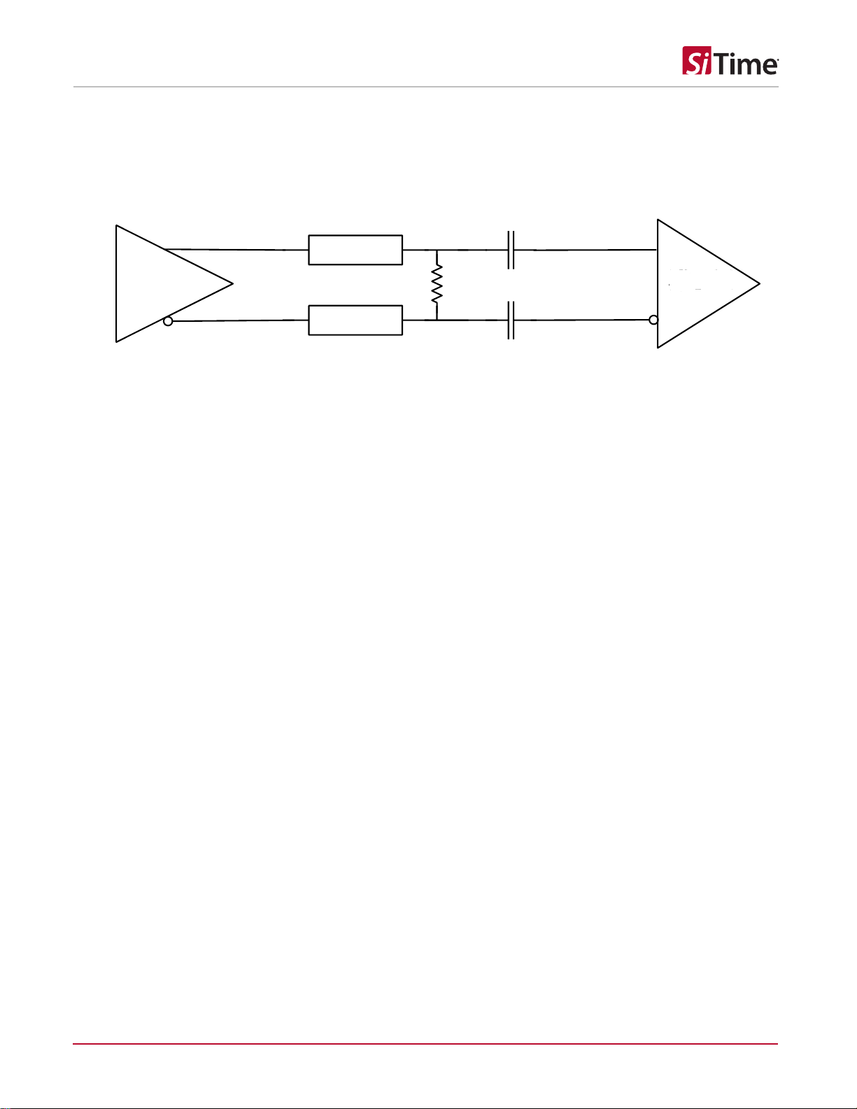
9 Driving Differential LVDS or LVDS Boost (AC coupled)
The input sees a 100
signal is followed by AC coupling capacitor of 0.1 uF. So, no change in board configuration is required.
Figure 7. LVDS or LVDS Boost AC coupled

SiT92113 Ultra Low Jitter Buffer Evaluation Kit User Guide
SiT92113EB User Manual | Rev 0.5
Page 12 of 24
www.sitime.com
10 Board Configuration for driving DC Coupled LVDS
10.1.LVDS (DC coupled)
Terminate with a differential 100 Figure 8.
Figure 8. Termination scheme for DC coupled LVDS
10.2.Board Changes Required for DC Coupled LVDS
Table 12. Board changes required for DC coupled LVDS or LVDS Boost
Clock 0 Path
C149
change to 0 Ohms
Schematic Sheet 7
C150
change to 0 Ohms

SiT92113 Ultra Low Jitter Buffer Evaluation Kit User Guide
SiT92113EB User Manual | Rev 0.5
Page 13 of 24
www.sitime.com
11 Board Configuration Required for Driving DC/AC coupled LVPECL
11.1.DC/AC Coupled LVPECL
The LVPECL standard requires a DC path for the input clock driver. The 50 -
2 V. The VCM (VCC-2 V) need to be capable of sinking or sourcing current. There is a provision to provide VCM in the input
clock circuit through jumper J90, J91.
So, no board changes are required but just give VCM through jumpers J90, J91.
Figure 9. Termination scheme for DC coupled LVPECL
SiT92113 Ultra Low Jitter Buffer Evaluation Kit User Guide
SiT92113EB User Manual | Rev 0.5
Page 14 of 24
www.sitime.com
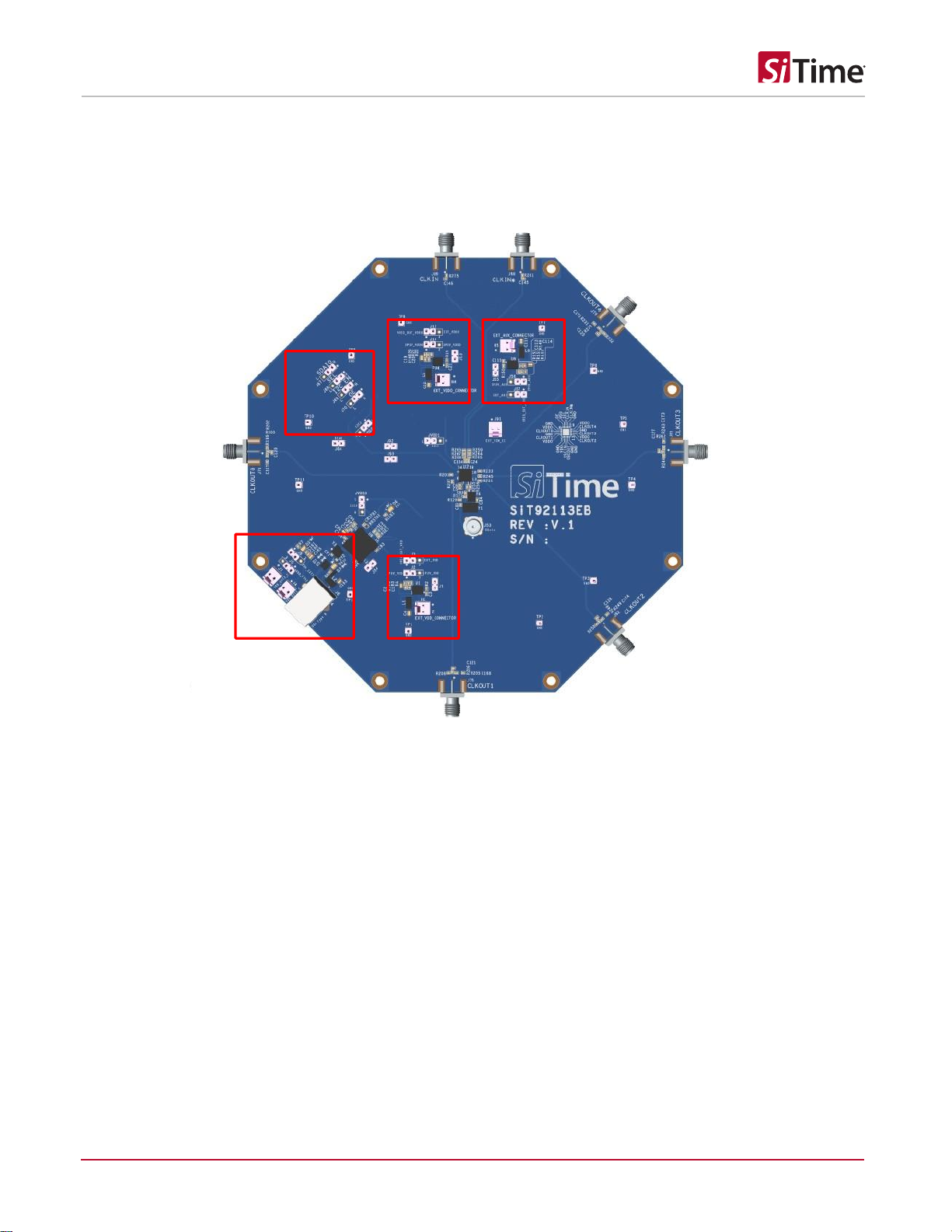
12 EVB Snapshot
Figure 10. EVB Snapshot
Block 1 has jumper settings to configure chip VDD as mentioned in Table 5
Block 2 has jumper settings to configure chip VDDO as mentioned in Table 6.
Block 3 has jumper settings to configure chip VDD_AUX as mentioned in

SiT92113 Ultra Low Jitter Buffer Evaluation Kit User Guide
SiT92113EB User Manual | Rev 0.5
Page 15 of 24
www.sitime.com
Table 7.
Block 4 has jumpers to select Clock inputs (SEL) and to set OE as mentioned in Table 8
Block 5 has USB port to power up the board or to select jumper for power up using external supply as mentioned in Table 4.


Table of contents
Other SiTime Motherboard manuals

SiTime
SiTime SiT6760EB User manual

SiTime
SiTime SiT6502EB User manual

SiTime
SiTime Time Machine II User manual

SiTime
SiTime SiT6098EBB User manual

SiTime
SiTime SiT92216 User manual

SiTime
SiTime SiT95314 User manual

SiTime
SiTime SiT6722EB User manual

SiTime
SiTime SiT6712EB User manual

SiTime
SiTime SiT6722EB User manual

SiTime
SiTime SiT6503EB User manual


