SMSC USB2513i User manual

SMSC USB2513i DATASHEET Revision1.98(11-19-07)
Datasheet
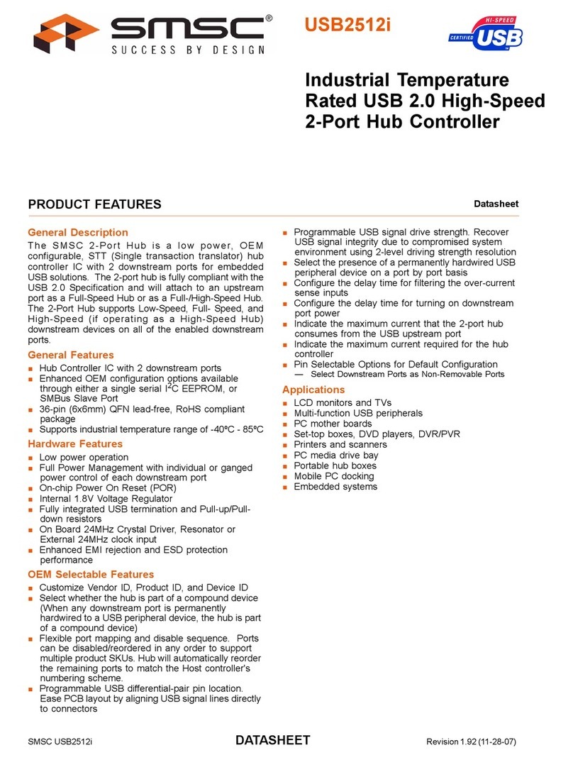
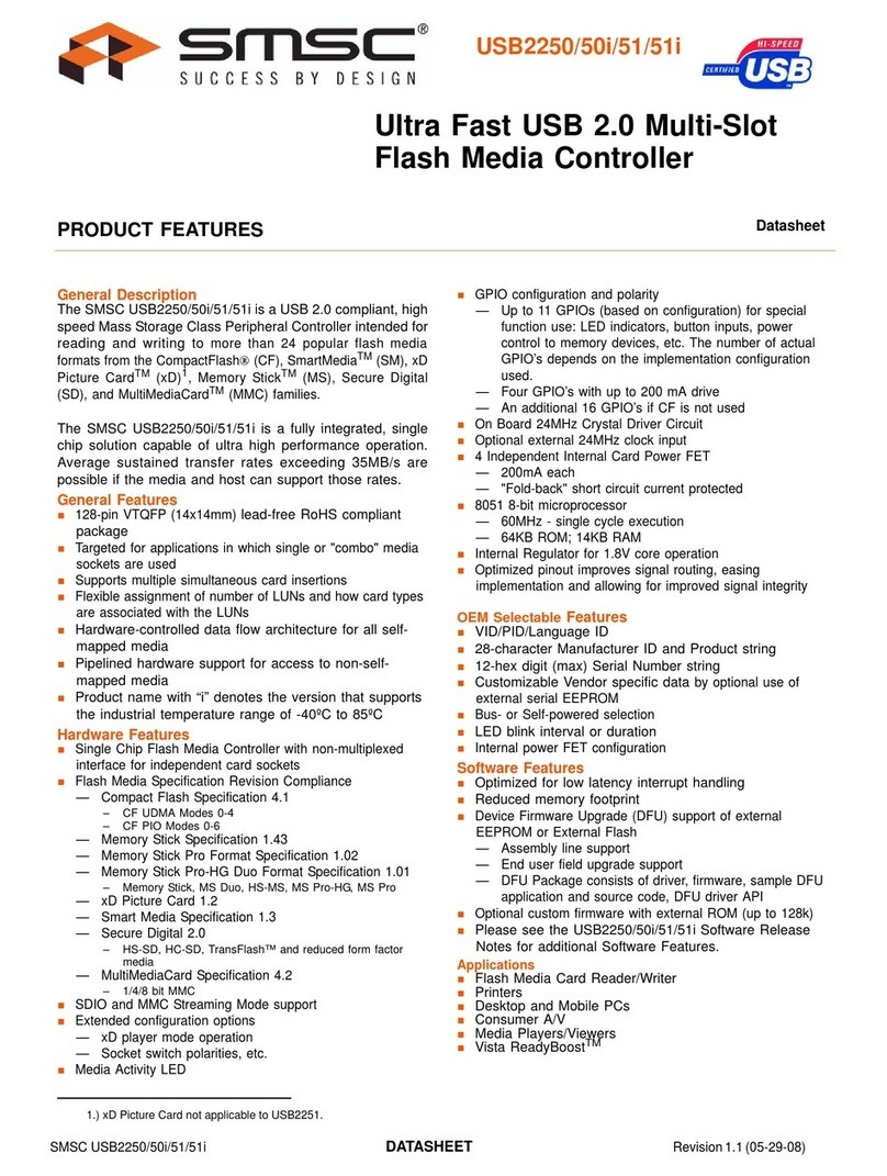
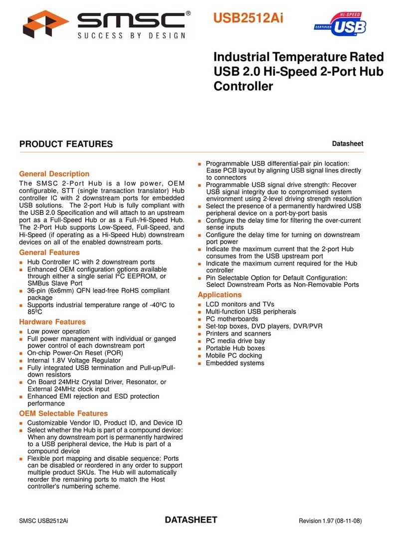
PRODUCT FEATURES
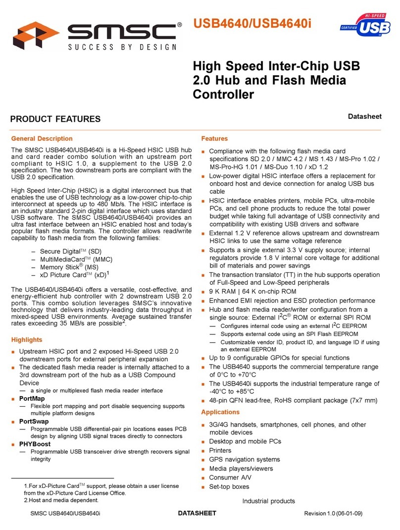
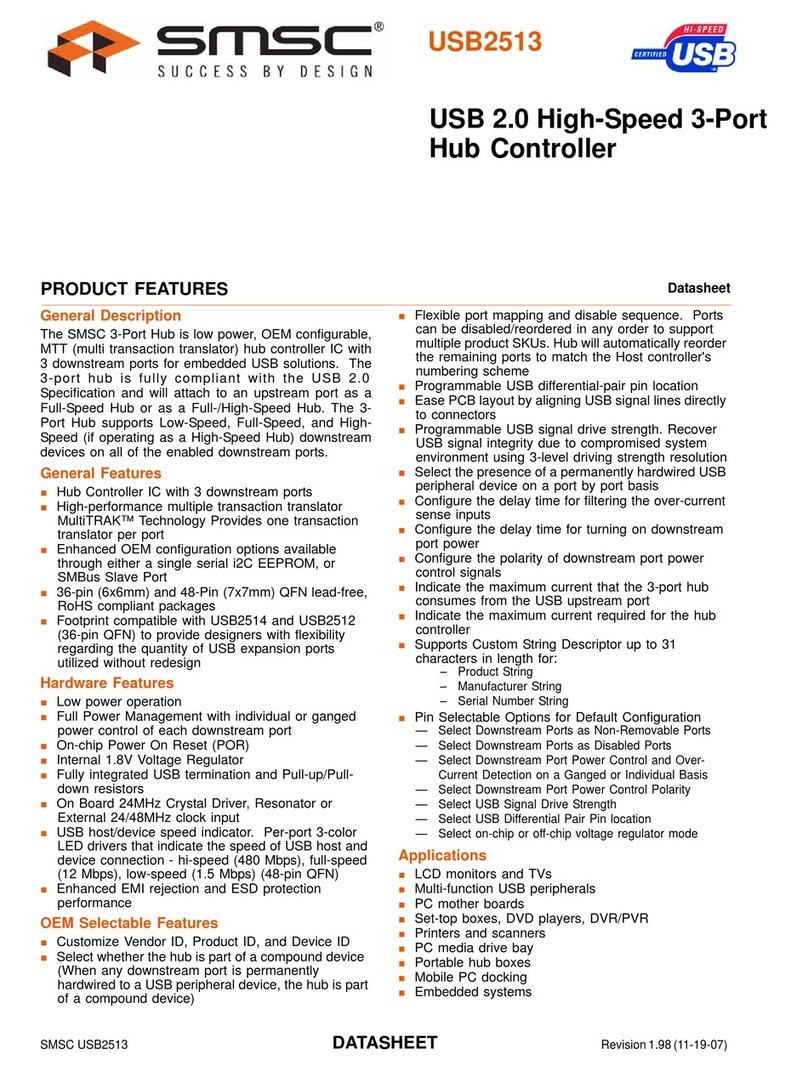
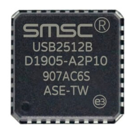
USB2513i
Industrial Temperature
Rated USB 2.0 High-Speed
3-Port Hub Controller
General Description
The SMSC 3-Port Hub is low power, OEM configurable,
MTT (multi transaction translator) hub controller IC with
3 downstream ports for embedded USB solutions. The
3-port hub is fully compliant with the USB 2.0
Specification and will attach to an upstream port as a
Full-Speed Hub or as a Full-/High-Speed Hub. The 3-
Port Hub supports Low-Speed, Full-Speed, and High-
Speed (if operating as a High-Speed Hub) downstream
devices on all of the enabled downstream ports.
General Features
Hub Controller IC with 3 downstream ports
High-performance multiple transaction translator
MultiTRAK™ Technology Provides one transaction
translator per port
Enhanced OEM configuration options available
through either a single serial i2C EEPROM, or
SMBus Slave Port
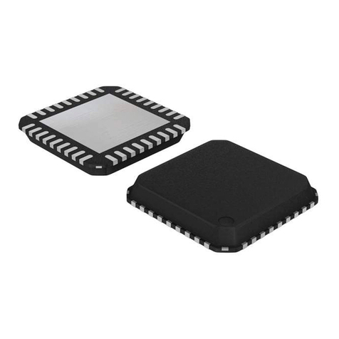
36-pin (6x6mm) and 48-Pin (7x7mm) QFN lead-free,
RoHS compliant packages
Footprint compatible with USB2514i and USB2512i
(36-pin QFN) to provide designers with flexibility
regarding the quantity of USB expansion ports
utilized without redesign
Supports industrial temperature range of -40ºC to
85ºC
Hardware Features
Low power operation
Full Power Management with individual or ganged
power control of each downstream port
On-chip Power On Reset (POR)
Internal 1.8V Voltage Regulator
Fully integrated USB termination and Pull-up/Pull-
down resistors
On Board 24MHz Crystal Driver, Resonator or
External 24/48MHz clock input
USB host/device speed indicator. Per-port 3-color
LED drivers that indicate the speed of USB host and
device connection - hi-speed (480 Mbps), full-speed
(12 Mbps), low-speed (1.5 Mbps) (48-pin QFN)
Enhanced EMI rejection and ESD protection
performance
OEM Selectable Features
Customize Vendor ID, Product ID, and Device ID
Select whether the hub is part of a compound device
(When any downstream port is permanently
hardwired to a USB peripheral device, the hub is part
of a compound device)
Flexible port mapping and disable sequence. Ports
can be disabled/reordered in any order to support
multiple product SKUs. Hub will automatically reorder
the remaining ports to match the Host controller's
numbering scheme
Programmable USB differential-pair pin location
Ease PCB layout by aligning USB signal lines directly
to connectors
Programmable USB signal drive strength. Recover
USB signal integrity due to compromised system
environment using 3-level driving strength resolution
Select the presence of a permanently hardwired USB
peripheral device on a port by port basis
Configure the delay time for filtering the over-current
sense inputs
Configure the delay time for turning on downstream
port power
Configure the polarity of downstream port power
control signals
Indicate the maximum current that the 3-port hub
consumes from the USB upstream port
Indicate the maximum current required for the hub
controller
Supports Custom String Descriptor up to 31
characters in length for:
– Product String
– Manufacturer String
– Serial Number String
Pin Selectable Options for Default Configuration
— Select Downstream Ports as Non-Removable Ports
— Select Downstream Ports as Disabled Ports
— Select Downstream Port Power Control and Over-
Current Detection on a Ganged or Individual Basis
— Select Downstream Port Power Control Polarity
— Select USB Signal Drive Strength
— Select USB Differential Pair Pin location
— Select on-chip or off-chip voltage regulator mode
Applications
LCD monitors and TVs
Multi-function USB peripherals
PC mother boards
Set-top boxes, DVD players, DVR/PVR
Printers and scanners
PC media drive bay
Portable hub boxes
Mobile PC docking
Embedded systems

ORDER NUMBERS:
USB2513i-AEZG FOR 36 PIN, QFN LEAD-FREE ROHS COMPLIANT PACKAGE
USB2513i-HZH FOR 48 PIN, QFN LEAD-FREE ROHS COMPLIANT PACKAGE
Industrial Temperature Rated USB 2.0 High-Speed 3-Port Hub Controller
Datasheet
Revision 1.98 (11-19-07) 2 SMSC USB2513i
DATASHEET
80 ARKAY DRIVE, HAUPPAUGE, NY 11788 (631) 435-6000, FAX (631) 273-3123
Copyright © 2007 SMSC or its subsidiaries. All rights reserved.
Circuit diagrams and other information relating to SMSC products are included as a means of illustrating typical applications. Consequently, complete information sufficient for
construction purposes is not necessarily given. Although the information has been checked and is believed to be accurate, no responsibility is assumed for inaccuracies. SMSC
reserves the right to make changes to specifications and product descriptions at any time without notice. Contact your local SMSC sales office to obtain the latest specifications
before placing your product order. The provision of this information does not convey to the purchaser of the described semiconductor devices any licenses under any patent
rights or other intellectual property rights of SMSC or others. All sales are expressly conditional on your agreement to the terms and conditions of the most recently dated
version of SMSC's standard Terms of Sale Agreement dated before the date of your order (the "Terms of Sale Agreement"). The product may contain design defects or errors
known as anomalies which may cause the product's functions to deviate from published specifications. Anomaly sheets are available upon request. SMSC products are not
designed, intended, authorized or warranted for use in any life support or other application where product failure could cause or contribute to personal injury or severe property
damage. Any and all such uses without prior written approval of an Officer of SMSC and further testing and/or modification will be fully at the risk of the customer. Copies of
this document or other SMSC literature, as well as the Terms of Sale Agreement, may be obtained by visiting SMSC’s website at http://www.smsc.com. SMSC is a registered
trademark of Standard Microsystems Corporation (“SMSC”). Product names and company names are the trademarks of their respective holders.
SMSC DISCLAIMS AND EXCLUDES ANY AND ALL WARRANTIES, INCLUDING WITHOUT LIMITATION ANY AND ALL IMPLIED WARRANTIES OF MERCHANTABILITY,
FITNESS FOR A PARTICULAR PURPOSE, TITLE, AND AGAINST INFRINGEMENT AND THE LIKE, AND ANY AND ALL WARRANTIES ARISING FROM ANY COURSE
OF DEALING OR USAGE OF TRADE. IN NO EVENT SHALL SMSC BE LIABLE FOR ANY DIRECT, INCIDENTAL, INDIRECT, SPECIAL, PUNITIVE, OR CONSEQUENTIAL
DAMAGES; OR FOR LOST DATA, PROFITS, SAVINGS OR REVENUES OF ANY KIND; REGARDLESS OF THE FORM OF ACTION, WHETHER BASED ON CONTRACT;
TORT; NEGLIGENCE OF SMSC OR OTHERS; STRICT LIABILITY; BREACH OF WARRANTY; OR OTHERWISE; WHETHER OR NOT ANY REMEDY OF BUYER IS HELD
TO HAVE FAILED OF ITS ESSENTIAL PURPOSE, AND WHETHER OR NOT SMSC HAS BEEN ADVISED OF THE POSSIBILITY OF SUCH DAMAGES.

Industrial Temperature Rated USB 2.0 High-Speed 3-Port Hub Controller
Datasheet
SMSC USB2513i 3 Revision 1.98 (11-19-07)
DATASHEET
Table of Contents
Chapter 1 Pin Configuration . . . . . . . . . . . . . . . . . . . . . . . . . . . . . . . . . . . . . . . . . . . . . . . . . . 6
Chapter 2 Block Diagram . . . . . . . . . . . . . . . . . . . . . . . . . . . . . . . . . . . . . . . . . . . . . . . . . . . . . 8
Chapter 3 Pin Descriptions . . . . . . . . . . . . . . . . . . . . . . . . . . . . . . . . . . . . . . . . . . . . . . . . . . . . 9
3.1 PIN Descriptions. . . . . . . . . . . . . . . . . . . . . . . . . . . . . . . . . . . . . . . . . . . . . . . . . . . . . . . . . . . . . . . . 9
3.2 Buffer Type Descriptions . . . . . . . . . . . . . . . . . . . . . . . . . . . . . . . . . . . . . . . . . . . . . . . . . . . . . . . . 16
Chapter 4 Configuration Options. . . . . . . . . . . . . . . . . . . . . . . . . . . . . . . . . . . . . . . . . . . . . . 18
4.1 3-Port Hub . . . . . . . . . . . . . . . . . . . . . . . . . . . . . . . . . . . . . . . . . . . . . . . . . . . . . . . . . . . . . . . . . . . 18
4.1.1 Hub Configuration Options . . . . . . . . . . . . . . . . . . . . . . . . . . . . . . . . . . . . . . . . . . . . . . . 18
4.1.2 VBus Detect. . . . . . . . . . . . . . . . . . . . . . . . . . . . . . . . . . . . . . . . . . . . . . . . . . . . . . . . . . . 18
4.2 36 QFN and 48 QFN Feature Differences . . . . . . . . . . . . . . . . . . . . . . . . . . . . . . . . . . . . . . . . . . . 18
4.3 EEPROM Interface. . . . . . . . . . . . . . . . . . . . . . . . . . . . . . . . . . . . . . . . . . . . . . . . . . . . . . . . . . . . . 19
4.3.1 Internal Register Set (Common to EEPROM and SMBus) . . . . . . . . . . . . . . . . . . . . . . . 19
4.3.2 I2C EEPROM . . . . . . . . . . . . . . . . . . . . . . . . . . . . . . . . . . . . . . . . . . . . . . . . . . . . . . . . . 33
4.3.3 In-Circuit EEPROM Programming. . . . . . . . . . . . . . . . . . . . . . . . . . . . . . . . . . . . . . . . . . 33
4.4 SMBus Slave Interface . . . . . . . . . . . . . . . . . . . . . . . . . . . . . . . . . . . . . . . . . . . . . . . . . . . . . . . . . . 34
4.4.1 Bus Protocols . . . . . . . . . . . . . . . . . . . . . . . . . . . . . . . . . . . . . . . . . . . . . . . . . . . . . . . . . 34
4.4.2 Invalid Protocol Response Behavior . . . . . . . . . . . . . . . . . . . . . . . . . . . . . . . . . . . . . . . . 35
4.4.3 General Call Address Response . . . . . . . . . . . . . . . . . . . . . . . . . . . . . . . . . . . . . . . . . . . 35
4.4.4 Slave Device Time-Out . . . . . . . . . . . . . . . . . . . . . . . . . . . . . . . . . . . . . . . . . . . . . . . . . . 35
4.4.5 Stretching the SCLK Signal. . . . . . . . . . . . . . . . . . . . . . . . . . . . . . . . . . . . . . . . . . . . . . . 35
4.4.6 SMBus Timing . . . . . . . . . . . . . . . . . . . . . . . . . . . . . . . . . . . . . . . . . . . . . . . . . . . . . . . . . 35
4.4.7 Bus Reset Sequence. . . . . . . . . . . . . . . . . . . . . . . . . . . . . . . . . . . . . . . . . . . . . . . . . . . . 36
4.4.8 SMBus Alert Response Address. . . . . . . . . . . . . . . . . . . . . . . . . . . . . . . . . . . . . . . . . . . 36
4.5 Default Configuration Option: . . . . . . . . . . . . . . . . . . . . . . . . . . . . . . . . . . . . . . . . . . . . . . . . . . . . . 36
4.6 Default Strapping Options: . . . . . . . . . . . . . . . . . . . . . . . . . . . . . . . . . . . . . . . . . . . . . . . . . . . . . . . 36
4.7 Reset . . . . . . . . . . . . . . . . . . . . . . . . . . . . . . . . . . . . . . . . . . . . . . . . . . . . . . . . . . . . . . . . . . . . . . . 37
4.7.1 Internal POR Hardware Reset. . . . . . . . . . . . . . . . . . . . . . . . . . . . . . . . . . . . . . . . . . . . . 37
4.7.2 External Hardware RESET_N . . . . . . . . . . . . . . . . . . . . . . . . . . . . . . . . . . . . . . . . . . . . . 37
4.7.3 USB Bus Reset . . . . . . . . . . . . . . . . . . . . . . . . . . . . . . . . . . . . . . . . . . . . . . . . . . . . . . . . 40
Chapter 5 DC Parameters. . . . . . . . . . . . . . . . . . . . . . . . . . . . . . . . . . . . . . . . . . . . . . . . . . . . 42
5.1 Maximum Guaranteed Ratings. . . . . . . . . . . . . . . . . . . . . . . . . . . . . . . . . . . . . . . . . . . . . . . . . . . . 42
5.2 Recommended Operating Conditions. . . . . . . . . . . . . . . . . . . . . . . . . . . . . . . . . . . . . . . . . . . . . . . 42
Chapter 6 AC Specifications. . . . . . . . . . . . . . . . . . . . . . . . . . . . . . . . . . . . . . . . . . . . . . . . . . 46
6.1 Oscillator/Clock. . . . . . . . . . . . . . . . . . . . . . . . . . . . . . . . . . . . . . . . . . . . . . . . . . . . . . . . . . . . . . . . 46
6.1.1 SMBus Interface:. . . . . . . . . . . . . . . . . . . . . . . . . . . . . . . . . . . . . . . . . . . . . . . . . . . . . . . 46
6.1.2 I2C EEPROM: . . . . . . . . . . . . . . . . . . . . . . . . . . . . . . . . . . . . . . . . . . . . . . . . . . . . . . . . . 46
6.1.3 USB 2.0 . . . . . . . . . . . . . . . . . . . . . . . . . . . . . . . . . . . . . . . . . . . . . . . . . . . . . . . . . . . . . . 46
Chapter 7 Package Outlines . . . . . . . . . . . . . . . . . . . . . . . . . . . . . . . . . . . . . . . . . . . . . . . . . . 47

Industrial Temperature Rated USB 2.0 High-Speed 3-Port Hub Controller
Datasheet
Revision 1.98 (11-19-07) 4 SMSC USB2513i
DATASHEET
List of Figures
Figure 1.1 USB2513i 36-Pin QFN. . . . . . . . . . . . . . . . . . . . . . . . . . . . . . . . . . . . . . . . . . . . . . . . . . . . . . . 6
Figure 1.2 USB2513i 48-Pin QFN. . . . . . . . . . . . . . . . . . . . . . . . . . . . . . . . . . . . . . . . . . . . . . . . . . . . . . . 7
Figure 2.1 USB2513i Block Diagram. . . . . . . . . . . . . . . . . . . . . . . . . . . . . . . . . . . . . . . . . . . . . . . . . . . . . 8
Figure 4.1 Block Write. . . . . . . . . . . . . . . . . . . . . . . . . . . . . . . . . . . . . . . . . . . . . . . . . . . . . . . . . . . . . . . 34
Figure 4.2 Block Read. . . . . . . . . . . . . . . . . . . . . . . . . . . . . . . . . . . . . . . . . . . . . . . . . . . . . . . . . . . . . . . 35
Figure 4.3 LED Strapping Option . . . . . . . . . . . . . . . . . . . . . . . . . . . . . . . . . . . . . . . . . . . . . . . . . . . . . . 37
Figure 4.4 Reset_N Timing for Default/Strap Option Mode. . . . . . . . . . . . . . . . . . . . . . . . . . . . . . . . . . . 38
Figure 4.5 Reset_N Timing for EEPROM Mode . . . . . . . . . . . . . . . . . . . . . . . . . . . . . . . . . . . . . . . . . . . 39
Figure 4.6 Reset_N Timing for SMBus Mode . . . . . . . . . . . . . . . . . . . . . . . . . . . . . . . . . . . . . . . . . . . . . 40
Figure 6.1 Typical Crystal Circuit . . . . . . . . . . . . . . . . . . . . . . . . . . . . . . . . . . . . . . . . . . . . . . . . . . . . . . 46
Figure 6.2 Formula to find value of C1 and C2 . . . . . . . . . . . . . . . . . . . . . . . . . . . . . . . . . . . . . . . . . . . . 46
Figure 7.1 36-Pin QFN, 6x6mm Body, 0.5mm Pitch. . . . . . . . . . . . . . . . . . . . . . . . . . . . . . . . . . . . . . . . 47
Figure 7.2 48-Pin QFN, 7x7mm Body, 0.5mm Pitch. . . . . . . . . . . . . . . . . . . . . . . . . . . . . . . . . . . . . . . . 48

Industrial Temperature Rated USB 2.0 High-Speed 3-Port Hub Controller
Datasheet
SMSC USB2513i 5 Revision 1.98 (11-19-07)
DATASHEET
List of Tables
Table 3.1 USB2514 Pin Descriptions . . . . . . . . . . . . . . . . . . . . . . . . . . . . . . . . . . . . . . . . . . . . . . . . . . . . 9
Table 3.2 SMBus or EEPROM Interface Behavior . . . . . . . . . . . . . . . . . . . . . . . . . . . . . . . . . . . . . . . . . 15
Table 3.3 USB2514 Power, Ground, No Connect. . . . . . . . . . . . . . . . . . . . . . . . . . . . . . . . . . . . . . . . . . 16
Table 3.4 USB2514 Buffer Type Descriptions. . . . . . . . . . . . . . . . . . . . . . . . . . . . . . . . . . . . . . . . . . . . . 16
Table 4.1 36 QFN and 48 QFN Feature Differences. . . . . . . . . . . . . . . . . . . . . . . . . . . . . . . . . . . . . . . . 18
Table 4.2 Internal Default, EEPROM and SMBus Register Memory Map. . . . . . . . . . . . . . . . . . . . . . . . 19
Table 4.3 Port Remap Register for Ports 1 & 2. . . . . . . . . . . . . . . . . . . . . . . . . . . . . . . . . . . . . . . . . . . . 31
Table 4.4 Port Remap Register for Port 3 . . . . . . . . . . . . . . . . . . . . . . . . . . . . . . . . . . . . . . . . . . . . . . . . 32
Table 4.5 Reset_N Timing for Default/Strap Option Mode . . . . . . . . . . . . . . . . . . . . . . . . . . . . . . . . . . . 38
Table 4.6 Reset_N Timing for EEPROM Mode. . . . . . . . . . . . . . . . . . . . . . . . . . . . . . . . . . . . . . . . . . . . 39
Table 4.7 Reset_N Timing for SMBus Mode. . . . . . . . . . . . . . . . . . . . . . . . . . . . . . . . . . . . . . . . . . . . . . 40
Table 5.1 DC Electrical Characteristics. . . . . . . . . . . . . . . . . . . . . . . . . . . . . . . . . . . . . . . . . . . . . . . . . . 43
Table 5.2 Pin Capacitance. . . . . . . . . . . . . . . . . . . . . . . . . . . . . . . . . . . . . . . . . . . . . . . . . . . . . . . . . . . . 45

Industrial Temperature Rated USB 2.0 High-Speed 3-Port Hub Controller
Datasheet
Revision 1.98 (11-19-07) 6 SMSC USB2513i
DATASHEET
Chapter 1 Pin Configuration
Figure 1.1 USB2513i 36-Pin QFN
Thermal Slug
(must be connected to VSS)
SMSC
USB2513i
(Top View QFN-36)
Indicates pins on the bottom of the device.
26
VDD33
25
RESET_N
24
HS_IND/CFG_SEL1
23
SCL/SMBCLK/CFG_SEL0
22 SDA/SMBDATA/NON_REM1
21 NC
20 NC
19
VBUS_DET
27
OCS3_N
18 PRTPWR3
17 OCS2_N
16 PRTPWR2
15
OCS1_N
14
VDD33CR
13
VDD18
12 PRTPWR1
11 TEST
10 VDDA33
SUSP_IND/LOCAL_PWR/NON_REM0 28
VDDA33 29
USBUP_DP 31
XTAL2 32
XTAL1/CLKIN 33
RBIAS
36
VDD33PLL
35
VDD18PLL 34
USBUP_DM 30
VDDA33
1
USBDN1_DM/PRT_DIS_M1
2
USBDN1_DP/PRT_DIS_P1
3
USBDN2_DM/PRT_DIS_M2
4
USBDN2_DP/PRT_DIS_P2
5
USBDN3_DM/PRT_DOS_M3 6
USBDN3_DP/PRT_DIS_P3 7
NC 8
NC 9

Industrial Temperature Rated USB 2.0 High-Speed 3-Port Hub Controller
Datasheet
SMSC USB2513i 7 Revision 1.98 (11-19-07)
DATASHEET
Figure 1.2 USB2513i 48-Pin QFN
Thermal Slug
(must be connected to VSS)
SMSC
USB2513i
(Top View QFN-48)
Indicates pins on the bottom of the device.
PRTPWR_POL 38
SUSP_IND/LOCAL_PWR/NON_REM0 39
LED_A1_N/PRT_SWP1 37
SEL48 40
VDDA33 41
USBUP_DP 43
XTAL2 44
XTAL1/CLKIN 45
RBIAS
48
VDD33PLL
47
VDD18PLL 46
USBUP_DM 42
VDDA33
1
USBDN1_DM/PRT_DIS_M1
2
USBDN1_DP/PRT_DIS_P1
3
USBDN2_DM/PRT_DIS_M2
4
USBDN2_DP/PRT_DIS_P2
5
USBDN3_DM/PRT_DIS_M3 6
USBDN3_DP/PRT_DIS_P3 7
NC 8
NC 9
NC
10
REG_EN 11
VDDA33
12
21 PRTPWR3
20 OCS2_N
19 PRTPWR2
18 VDD33CR
17
PRTPWR1
16
VDD18
15
OCS1_N
14 TEST
13 NC
23 LED_A3_N/PRT_SWP3
22 LED_B3_N/GANG_EN
24 LED_B2_N/BOOST1
35
LED_B1_N/BOOST0
34
VBUS_DET
33
RESET_N
32 HS_IND/CFG_SEL1
31 SCL/SMBCLK/CFG_SEL0
30 VDD33
29 SDA/SMBDATA/NON_REM1
28 NC
36
CFG_SEL2
27 NC
26 OCS3_N
25 LED_A2_N/PRT_SWP2

Industrial Temperature Rated USB 2.0 High-Speed 3-Port Hub Controller
Datasheet
Revision 1.98 (11-19-07) 8 SMSC USB2513i
DATASHEET
Chapter 2 Block Diagram
Figure 2.1 USB2513i Block Diagram
To Upstream
VBUS
3.3V
Upstream
PHY
Upstream USB
Data
Repeater Controller
SIE
Serial
Interface
PLL
24 MHz Crystal To EEPROM or
SMBus Master
Routing & Port Re-Ordering Logic
SCKSD
TT #3 Port
Controller
PHY#1
Port #1
OC
Sense
Switch
Driver
LED
Drivers
USB Data
Downstream OC Sense
Switch/LED
Drivers
Bus-Power
Detect/VBUS
Pulse
1.8V
TT #2TT #1
1.8V Reg
PHY#2
Port #2
OC
Sense
Switch
Driver
LED
Drivers
PHY#3
Port #3
OC
Sense
Switch
Driver
LED
Drivers
USB Data
Downstream OC Sense
Switch/LED
Drivers
USB Data
Downstream OC Sense
Switch/LED
Drivers

Industrial Temperature Rated USB 2.0 High-Speed 3-Port Hub Controller
Datasheet
SMSC USB2513i 9 Revision 1.98 (11-19-07)
DATASHEET
Chapter 3 Pin Descriptions
3.1 PIN Descriptions
This section provides a detailed description of each signal. The signals are arranged in functional
groups according to their associated interface.
The “N” symbol in the signal name indicates that the active, or asserted, state occurs when the signal
is at a low voltage level. When “N” is not present before the signal name, the signal is asserted when
at the high voltage level.
The terms assertion and negation are used exclusively. This is done to avoid confusion when working
with a mixture of “active low” and “active high” signals. The term assert, or assertion, indicates that a
signal is active, independent of whether that level is represented by a high or low voltage. The term
negate, or negation, indicates that a signal is inactive.
Table 3.1 USB2514 Pin Descriptions
SYMBOL 36 QFN 48 QFN BUFFER
TYPE DESCRIPTION
UPSTREAM USB INTERFACES
USBUP_DP
USBUP_DM 31
30 43
42 IO-U USB Bus Data
These pins connect to the upstream USB bus data
signals (Host port, or upstream hub).
VBUS_DET 27 35 I/O12 Detect Upstream VBUS Power
Detects state of Upstream VBUS power. The SMSC Hub
monitors VBUS_DET to determine when to assert the
internal D+ pull-up resistor (signaling a connect event).
When designing a detachable hub, this pin must be
connected to the VBUS power pin of the USB port that
is upstream of the hub.
For self-powered applications with a permanently
attached host, this pin must be connected to 3.3V
(typically VDD33).
DOWNSTREAM 3-PORT USB 2.0 INTERFACE
USBDN_DP[3:1]/
PRT_DIS_P[3:1]
&
USBDN_DM[3:1]/
PRT_DIS_M[3:1]
7
4
2
7
4
2
IO-U High-Speed USB Data & Port Disable Strap Option
These pins connect to the downstream USB peripheral
devices attached to the hub’s port.
6
3
1
6
3
1
Downstream Port Disable Strap option:
If this strap is enabled by package and configuration
settings (see Table 3.2), this pin will be sampled at
RESET_N negation to determine if the port is disabled.
Both USB data pins for the corresponding port must be
tied to the VDDA33 to disable the associated
downstream port.
PRTPWR[3:1] 18
16
12
21
19
15
O12 USB Power Enable
Enables power to USB peripheral devices downstream.
The active signal level of the PRTPWR[3:1] pins is
determined by the Power Polarity Strapping function of
the PRTPWR_POL pin.

Industrial Temperature Rated USB 2.0 High-Speed 3-Port Hub Controller
Datasheet
Revision 1.98 (11-19-07) 10 SMSC USB2513i
DATASHEET
LED_A[3:1]_N/
PRT_SWP[3:1] n/a 23
25
37
I/O12 Port LED Indicators & Port Swap strapping option
Indicator LED for ports 1-3. Will be active low when LED
support is enabled via EEPROM or SMBus.
If this strap is enabled by package and configuration
settings (see Table 3.2), this pin will be sampled at
RESET_N negation to determine the electrical
connection polarity of the downstream USB Port pins
(USB_DP and USB_DM).
Also, the active state of the LED will be determined as
follows:
‘0’ = Port Polarity is normal, and the LED is active high.
‘1’ = Port Polarity (for USB_DP and USB_DM) is
swapped, and the LED is active low.
LED_B3_N/
GANG_EN n/a 22 I/O12 Enhanced Port 3 LED & Gang Power and Overcurrent
Strap Option
Enhanced Indicator LED for port 3. Will be active low
when LED support is enabled via EEPROM or SMBus.
GANG_EN: Selects between Gang or Individual Port
power and Over Current sensing.
If this strap is enabled by package and configuration
settings (see Table 3.2), this pin will be sampled at
RESET_N negation to determine the mode as follows:
‘0’ = Individual sensing & switching, and LED_B3_N is
active high.
‘1’ = Ganged sensing & switching, and LED_B3_N is
active low.
LED_B[2:1]_N/
BOOST[1:0] n/a 24
36 I/O12 Enhanced Port [2:1] LED & Phy Boost strapping option
Enhanced Indicator LED for ports 1 & 2. Will be active
low when LED support is enabled via EEPROM or
SMBus.
Table 3.1 USB2514 Pin Descriptions (continued)
SYMBOL 36 QFN 48 QFN BUFFER
TYPE DESCRIPTION

Industrial Temperature Rated USB 2.0 High-Speed 3-Port Hub Controller
Datasheet
SMSC USB2513i 11 Revision 1.98 (11-19-07)
DATASHEET
BOOST[1:0], If this strap is enabled by package and
configuration settings (see Table 3.2), this pin will be
sampled at RESET_N negation to determine if all PHY
ports (upstream and downstream) operate at a normal
or boosted electrical level. Also, the active state of the
LEDs will be determined as follows:
See for BOOST values: Section 4.3.1.26, "Register F6h:
Boost_Up" and Section 4.3.1.27, "Register F8h:
Boost_3:0".
BOOST[1:0] = BOOST_IOUT[1:0]
BOOST[1:0] = ‘00’,
LED_B2_N is active high,
LED_B1_N is active high.
BOOST[1:0] = ‘01’,
LED_B2_N is active high,
LED_B1_N is active low.
BOOST[1:0] = ‘10’,
LED_B2_N is active low,
LED_B1_N is active high.
BOOST[1:0] = ‘11’,
LED_B2_N is active low,
LED_B1_N is active low.
PRTPWR_POL n/a 38 IPU Port Power Polarity strapping
Port Power Polarity strapping determination for the
active signal polarity of the [3:1]PRTPWR pins.
While RESET_N is asserted, the logic state of this pin
will (through the use of internal combinatorial logic)
determine the active state of the [3:1]PRTPWR pins in
order to ensure that downstream port power is not
inadvertently enabled to inactive ports during a
hardware reset.
When RESET_N is negated, the logic value will be
latched internally, and will retain the active signal polarity
for the PRTPWR[3:1] pins.
‘1’ = PRTPWR[3:1]_P/N pins have an active ‘high’
polarity
‘0’ = PRTPWR[3:1]_P/N pins have an active ‘low’
polarity
Warning: Active Low port power controllers may glitch
the downstream port power when system power is first
applied. Care should be taken when designing with
active low components!
Note: If PRTPWR_POL is not an available pin on the
package, the hub will support active high
power controllers only!
OCS[3:1]_N 19
17
13
26
20
16
IPU Over Current Sense
Input from external current monitor indicating an over-
current condition.
{Note: Contains internal pull-up to 3.3V supply}
Table 3.1 USB2514 Pin Descriptions (continued)
SYMBOL 36 QFN 48 QFN BUFFER
TYPE DESCRIPTION

Industrial Temperature Rated USB 2.0 High-Speed 3-Port Hub Controller
Datasheet
Revision 1.98 (11-19-07) 12 SMSC USB2513i
DATASHEET
RBIAS 35 47 I-R USB Transceiver Bias
A 12.0kΩ(+/- 1%) resistor is attached from ground to
this pin to set the transceiver’s internal bias settings.
SERIAL PORT INTERFACE
SDA/
SMBDATA/
NON_REM1
22 29 I/OSD12 Serial Data / SMB Data & Port Non Removable Strap
Option
NON_REM1: Non removable port strap option.
If this strap is enabled by package and configuration
settings (see Table 3.2), this pin will be sampled (in
conjunction withLOCAL_PWR/SUSP_IND/NON_REM0)
at RESET_N negation to determine if imports [3:1]
contain permanently attached (non-removable) devices:
NON_REM[1:0] = ‘00’, All ports are removable,
NON_REM[1:0] = ‘01’, Port 1 is nonremovable,
NON_REM[1:0] = ‘10’, Ports 1 & 2 are non-removable,
NON_REM[1:0] = ‘11’, Ports 1, 2 & 3 are non-removable
SCL/
SMBCLK/
CFG_SEL0
24 31 I/OSD12 Serial Clock (SCL)
SMBus Clock (SMBCLK)
Configuration Select_SEL0: The logic state of this
multifunction pin is internally latched on the rising edge
of RESET_N (RESET_N negation), and will determine
the hub configuration method as described in Table 3.2,
"SMBus or EEPROM Interface Behavior".
HS_IND/
CFG_SEL1 25 32 I/O12 High-Speed Upstream port indictor & Configuration
Programming Select
HS_IND: High Speed Indicator for upstream port
connection speed.
The active state of the LED will be determined as
follows:
CFG_SEL1 = ‘0’,
HS_IND is active high,
CFG_SEL1 = ‘1’,
HS_IND is active low,
‘Asserted’ = Hub is connected at HS
‘Negated’ = Hub is connected at FS
CFG_SEL1: The logic state of this pin is internally
latched on the rising edge of RESET_N (RESET_N
negation), and will determine the hub configuration
method as described in Table 3.2, "SMBus or EEPROM
Interface Behavior".
Table 3.1 USB2514 Pin Descriptions (continued)
SYMBOL 36 QFN 48 QFN BUFFER
TYPE DESCRIPTION

Industrial Temperature Rated USB 2.0 High-Speed 3-Port Hub Controller
Datasheet
SMSC USB2513i 13 Revision 1.98 (11-19-07)
DATASHEET
CFG_SEL2 n/a 33 I Configuration Programming Select
Note: This pin is not available in all packages; it is
held to a logic ‘0’ when not available
The logic state of this pin is internally latched on the
rising edge of RESET_N (RESET_N negation), and will
determine the hub configuration method as described in
Table 3.2, "SMBus or EEPROM Interface Behavior"
MISC
XTAL1/
CLKIN 33 45 ICLKx Crystal Input/External Clock Input
24MHz crystal or external clock input.
This pin connects to either one terminal of the crystal or
to an external 24/48MHz clock when a crystal is not
used.
Note: 48MHz only available in 48 QFN.
XTAL2 32 44 OCLKx Crystal Output
24MHz Crystal
This is the other terminal of the crystal, or pulled high
when an external clock source is used to drive
XTAL1/CLKIN. This output must not be used to drive
any external circuitry other than the crystal circuit.
RESET_N 26 34 IS RESET Input
The system can reset the chip by driving this input low.
The minimum active low pulse is 1 us.
When the RESET_N pin is pulled to VDD33, the internal
POR (Power on Reset) is enabled and no external reset
circuitry is required. The internal POR holds the internal
logic in reset until the power supplies are stable.
Table 3.1 USB2514 Pin Descriptions (continued)
SYMBOL 36 QFN 48 QFN BUFFER
TYPE DESCRIPTION

Industrial Temperature Rated USB 2.0 High-Speed 3-Port Hub Controller
Datasheet
Revision 1.98 (11-19-07) 14 SMSC USB2513i
DATASHEET
SUSP_IND/
LOCAL_PWR/
NON_REM0
28 39 I/O Active/Suspend status LED or Local-Power & Non
Removable Strap Option
Suspend Indicator: Indicates USB state of the hub.
‘negated’ = Unconfigured, or configured and in USB
Suspend
‘asserted’ = Hub is configured, and is active (i.e., not in
suspend)
Local Power: Detects availability of local self-power
source.
Low = Self/local power source is NOT available (i.e.,
Hub gets all power from Upstream USB VBus).
High = Self/local power source is available.
NON_REM0 Strap Option:
If this strap is enabled by package and configuration
settings (see Table 3.2), this pin will be sampled (in
conjunction with NON_REM1) at RESET_N negation to
determine if ports [3:1] contain permanently attached
(non-removable) devices. Also, the active state of the
LED will be determined as follows:
NON_REM[1:0] = ‘00’, All ports are removable, and the
LED is active high
NON_REM[1:0] = ‘01’, Port 1 is nonremovable, and the
LED is active low
NON_REM[1:0] = ‘10’, Ports 1 & 2 are non-removable,
and the LED is active high
NON_REM[1:0] = ‘11’, Ports 1, 2 & 3 are non-
removable, and the LED is active low
TEST 11 14 IPD TEST pin
XNOR continuity tests all signal pins on the hub, please
contact your SMSC representative for a detailed
description of how this test mode is enabled and utilized.
SEL48 n/a 40 I Select 48 MHz clock input
48MHz external clock input select. When the hub is
clocked from an external clock source, this pin selects
either 24MHz or 48MHz mode.
‘0’ = 24MHz
‘1’ = 48MHz
REG_EN n/a 11 IPU Regulator Enable
REG_EN: This pin is internally pulled up to enable the
internal 1.8V regulators, and this pin should be treated
as a no-connect.
In order to disable the regulators, this pin will need to be
externally connected to ground.
When the internal regulator is enabled, the 1.8V power
pins must be left unconnected, except for the required
bypass capacitors.
Table 3.1 USB2514 Pin Descriptions (continued)
SYMBOL 36 QFN 48 QFN BUFFER
TYPE DESCRIPTION

Industrial Temperature Rated USB 2.0 High-Speed 3-Port Hub Controller
Datasheet
SMSC USB2513i 15 Revision 1.98 (11-19-07)
DATASHEET
Notes:
Table 3.2 SMBus or EEPROM Interface Behavior
CFG_SEL2 CFG_SEL1 CFG_SEL0 SMBUS OR EEPROM INTERFACE BEHAVIOR
36-Pin
QFN N/A 00 Internal Default Configuration
Strap Options Enabled
Port Indicators Not Supported
48-Pin
QFN 00 0
36-Pin
QFN N/A 01 Configured as an SMBus slave for external download
of user-defined descriptors.
SMBus slave address 58 (0101100x)
Strap Options Disabled
All Settings Controlled by Registers
48-Pin
QFN 00 1
36-Pin
QFN N/A 10 Internal Default Configuration
Strap Options Enabled
Bus Power Operation
LED Mode = USB
48-Pin
QFN 01 0
36-Pin
QFN N/A 11 2-Wire I2C EEPROMS are supported.
Strap Options Disabled
All Settings Controlled by Registers
48-Pin
QFN 01 1
48-Pin
QFN 1 0 0 Internal Default Configuration
Strap Options Disabled
Dynamic Power Switching Enabled
48-Pin
QFN 1 0 1 Internal Default Configuration
Strap Options Disabled
Dynamic Power Switching Enabled
LED Mode = USB
48-Pin
QFN 1 1 0 Internal Default Configuration
Strap Options Disabled
48-Pin
QFN 1 1 1 Internal Default Configuration
Strap Options Disabled
LED Mode = USB
Ganged Power Switching
Ganged Over-Current Sensing
Denotes 48-Pin QFN Denotes 36-Pin QFN

Industrial Temperature Rated USB 2.0 High-Speed 3-Port Hub Controller
Datasheet
Revision 1.98 (11-19-07) 16 SMSC USB2513i
DATASHEET
3.2 Buffer Type Descriptions
Table 3.3 USB2514 Power, Ground, No Connect
PACKAGE
SYMBOL 36 QFN 48 QFN FUNCTION
VDD18 14 17 VDD Core
+1.8V core power. If the internal regulator is enabled, then this pin
must have a 1.0μF (or greater) ±20% (ESR <0.1Ω) capacitor to
VSS.
VDD33PLL 36 48 VDD 3.3 PLL Regulator Reference
+3.3V power supply for the PLL. If the internal PLL 1.8V regulator
is enabled, then this pin acts as the regulator input.
VDDPLL18 34 46 VDD PLL
+1.8V Filtered analog power for internal PLL. If the internal
regulator is enabled, then this pin must have a 1.0μF (or greater)
±20% (ESR <0.1Ω) capacitor to VSS.
VDDA33 5
10
29
5
10
41
VDD Analog I/O
+3.3V Filtered analog PHY power, shared between adjacent ports.
VDD33/VDD33CR 23
15 30
18 VDDIO/VDD 3.3 Core Regulator Reference
+3.3V power supply for the Digital I/O
If the internal core regulator is enabled, then VDD33CR acts as
the regulator input.
VSS n/a n/a VSS
Ground
Table 3.4 USB2514 Buffer Type Descriptions
BUFFER DESCRIPTION
I Input.
IPD Input with internal weak pull-down resistor.
IPU Input with internal weak pull-up resistor.
IS Input with Schmitt trigger.
O12 Output 12mA.
OD12 Open drain... 12mA sink.
I/O12 Input/Output buffer with 12mA sink and 12mA source.

Industrial Temperature Rated USB 2.0 High-Speed 3-Port Hub Controller
Datasheet
SMSC USB2513i 17 Revision 1.98 (11-19-07)
DATASHEET
I/OSD12 Open drain...12mA sink with Schmitt trigger, and must meet I2C-Bus Specification
Version 2.1 requirements.
ICLKx XTAL clock input.
OCLKx XTAL clock output.
I-R RBIAS.
I/O-U Analog Input/Output Defined in USB specification.
AIO Analog Input/Output.
Table 3.4 USB2514 Buffer Type Descriptions (continued)
BUFFER DESCRIPTION

Industrial Temperature Rated USB 2.0 High-Speed 3-Port Hub Controller
Datasheet
Revision 1.98 (11-19-07) 18 SMSC USB2513i
DATASHEET
Chapter 4 Configuration Options
4.1 3-Port Hub
SMSC’s USB 2.0 3-Port Hub is fully specification compliant to the Universal Serial Bus Specification
Revision 2.0 April 27, 2000 (12/7/2000 and 5/28/2002 Errata). Please reference Chapter 10 (Hub
Specification) for general details regarding Hub operation and functionality.
For performance reasons, the 3-Port Hub provides 1 Transaction Translator (TT) per port (defined as
Multi-TT configuration), divided into 4 non-periodic buffers per TT.
4.1.1 Hub Configuration Options
The SMSC Hub supports a large number of features (some are mutually exclusive), and must be
configured in order to correctly function when attached to a USB host controller. There are three
principal ways to configure the hub: SMBus, EEPROM, or by internal default settings (with or without
pin strapping option over-rides). In all cases, the configuration method will be determined by the
CFG_SEL2, CFG_SEL1 and CFG_SEL0 pins immediately after RESET_N negation.
4.1.1.1 Power Switching Polarity
The selection of active state “polarity” for the PRTPWR pins is made by a strapping option only (the
PRTPWR_POL pin).
Note: If PRTPWR_POL is not an available pin on the package, the hub will support active high power
controllers only!
4.1.2 VBus Detect
According to Section 7.2.1 of the USB 2.0 Specification, a downstream port can never provide power
to its D+ or D- pull-up resistors unless the upstream port’s VBUS is in the asserted (powered) state.
The VBUS_DET pin on the Hub monitors the state of the upstream VBUS signal and will not pull-up
the D+ resistor if VBUS is not active. If VBUS goes from an active to an inactive state (Not Powered),
Hub will remove power from the D+ pull-up resistor within 10 seconds.
4.2 36 QFN and 48 QFN Feature Differences
Table 4.1 36 QFN and 48 QFN Feature Differences
36 QFN 48 QFN FEATURE
N/A Available 48MHz clock input mode
N/A Available External 1.8V regulators
N/A Available Port LED Indicators
N/A Available Port Swap Strapping Options
Available N/A Only Active High Port Power Control is supported in 36 QFN package
Available N/A Boost Default Level is used; see Table 4.2, "Internal Default, EEPROM and
SMBus Register Memory Map"

Industrial Temperature Rated USB 2.0 High-Speed 3-Port Hub Controller
Datasheet
SMSC USB2513i 19 Revision 1.98 (11-19-07)
DATASHEET
4.3 EEPROM Interface
The SMSC Hub can be configured via a 2-wire (I2C) EEPROM (256x8). (Please see Table 3.1 for
specific details on how to enable configuration via an I2C EEPROM).
The Internal state-machine will (when configured for EEPROM support) read the external EEPROM for
configuration data. The hub will then “attach” to the upstream USB host.
Note: The Hub does not have the capacity to write, or “Program,” an external EEPROM. The Hub
only has the capability to read external EEPROMs. The external eeprom will be read (even if
it is blank or non-populated), and the hub will be “configured” with the values that are read.
Please see Internal Register Set (Common to EEPROM and SMBus) for a list of data fields available.
4.3.1 Internal Register Set (Common to EEPROM and SMBus)
Table 4.2 Internal Default, EEPROM and SMBus Register Memory Map
REG
ADDR R/W REGISTER NAME ABBR INTERNAL
DEFAULT ROM
SMBUS AND
EEPROM POR
VALUES
00h R/W VID LSB VIDL 24h 0x00
01h R/W VID MSB VIDM 04h 0x00
02h R/W PID LSB PIDL 13h 0x00
03h R/W PID MSB PIDM 25h 0x00
04h R/W DID LSB DIDL 00h 0x00
05h R/W DID MSB DIDM 00h 0x00
06h R/W Config Data Byte 1 CFG1 9Bh 0x00
07h R/W Config Data Byte 2 CFG2 10h 0x00
08h R/W Config Data Byte 3 CFG3 00h 0x00
09h R/W Non-Removable Devices NRD 00h 0x00
0Ah R/W Port Disable (Self) PDS 00h 0x00
0Bh R/W Port Disable (Bus) PDB 00h 0x00
0Ch R/W Max Power (Self) MAXPS 01h 0x00
0Dh R/W Max Power (Bus) MAXPB 64h 0x00
0Eh R/W Hub Controller Max Current
(Self) HCMCS 01h 0x00
0Fh R/W Hub Controller Max Current
(Bus) HCMCB 64h 0x00
10h R/W Power-on Time PWRT 32h 0x00
11h R/W LANG_ID_H LANGIDH 00h 0x00
12h R/W LANG_ID_L LANGIDL 00h 0x00
13h R/W MFR_STR_LEN MFRSL 00h 0x00
14h R/W PRD_STR_LEN PRDSL 00h 0x00

Industrial Temperature Rated USB 2.0 High-Speed 3-Port Hub Controller
Datasheet
Revision 1.98 (11-19-07) 20 SMSC USB2513i
DATASHEET
4.3.1.1 Register 00h: Vendor ID (LSB)
4.3.1.2 Register 01h: Vendor ID (MSB)
15h R/W SER_STR_LEN SERSL 00h 0x00
16h-53h R/W MFR_STR MANSTR 00h 0x00
54h-91h R/W PROD_STR PRDSTR 00h 0x00
92h-Cfh R/W SER_STR SERSTR 00h 0x00
D0h-F5h R/W Reserved N/A 01h 0x00
F6h R/W Boost_Up BOOSTUP 00h 0x00
F7h R/W Reserved N/A 00h 0x00
F8h R/W Boost_3:0 BOOST30 00h 0x00
F9h R/W Reserved N/A 00h 0x00
FAh R/W Port Swap PRTSP 00h 0x00
FBh R/W Port Remap 12 PRTR12 00h 0x00
FCh R/W Port Remap 3 PRTR3 00h 0x00
FDh-FEh R/W Reserved N/A 00h 0x00
FFh R/W Status/Command
Note: SMBus register
only
STCD 00h 0x00
BIT
NUMBER BIT NAME DESCRIPTION
7:0 VID_LSB Least Significant Byte of the Vendor ID. This is a 16-bit value that uniquely
identifies the Vendor of the user device (assigned by USB-Interface Forum).
This field is set by the OEM using either the SMBus or EEPROM interface
options.
BIT
NUMBER BIT NAME DESCRIPTION
7:0 VID_MSB Most Significant Byte of the Vendor ID. This is a 16-bit value that uniquely
identifies the Vendor of the user device (assigned by USB-Interface Forum).
This field is set by the OEM using either the SMBus or EEPROM interface
options.
Table 4.2 Internal Default, EEPROM and SMBus Register Memory Map (continued)
REG
ADDR R/W REGISTER NAME ABBR INTERNAL
DEFAULT ROM
SMBUS AND
EEPROM POR
VALUES
Table of contents
Other SMSC Controllers manuals
Popular Controllers manuals by other brands
Hanna Instruments
Hanna Instruments HI 504 instruction manual
United Enertech
United Enertech CR Installation and maintenance instructions
Linear Technology
Linear Technology Analog Devices LT8708-1 datasheet
MachMotion
MachMotion Apollo III 1000 Series manual
D-NAIL
D-NAIL 1.4 instructions

Pego
Pego 200NDINFSC User and maintenance manual
Mitsubishi
Mitsubishi MELSEC Q Series user manual
Altronix
Altronix Maximal series installation guide
Iseo
Iseo Zero1 Atlas Plus installation guide
Vimar
Vimar EIKON 20594.0 quick start guide
Synergy 21
Synergy 21 SR-1006 Series quick start guide
Mannesmann Rexroth
Mannesmann Rexroth Indramat ECODRIVE DKC01.1 Project planning manual
