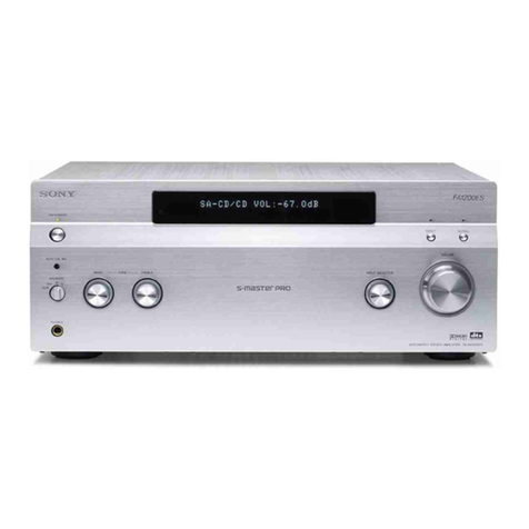
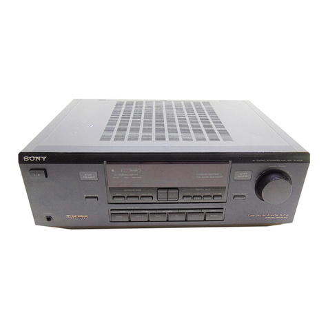
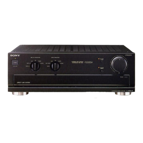
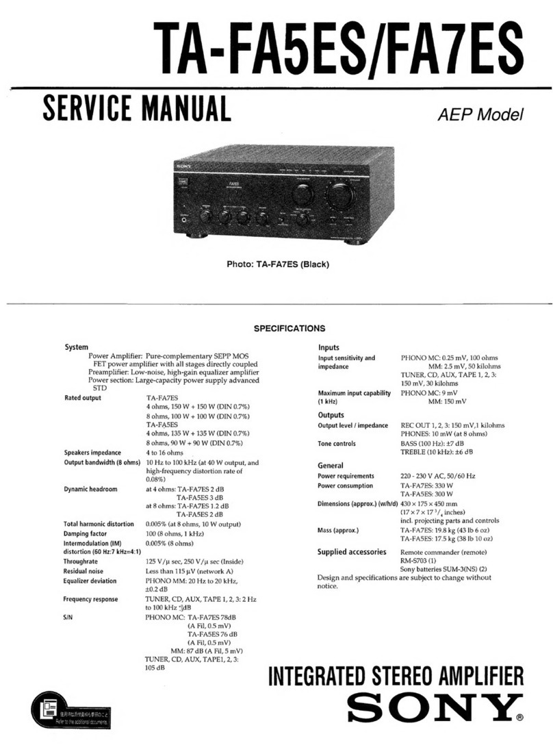
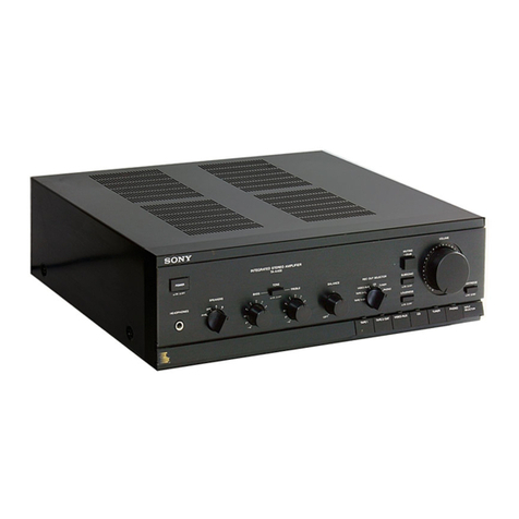
Sony TA-AV411 User manual

SERVICE
MANUAL
TA-AV411
US
Model
SPECIFICATIONS
AUDIO
POWER
SPECIFICATIONS
POWER
OUTPUT
AND
TOTAL
HARMONIC
DISTORTION:
With
8-ohm
loads,
both
channels
driven,
from
40
-
20,000
Hz;
rated
135
watts
per
channel
minimum
RMS
power,
with
less
than
0.9%
total
harmonic
distortion
from
250
milliwatts
to
rated
output.
Amplifier
section
Power
bandwidth
(IHF)
30
Hz
—
30
kHz
(8
ohms)
Dynamic
headroom
1.7
dB
(‘78
IHF)
Harmonic
distortion
Less
than
0.9%
at
rated
output
(Surround
OFF)
Frequency
response
PHONO:
RIAA
equalization
curve
CD,
VIDEO,
TUNER,
TAPE:
30
Hz
~-
30
KHz
+3dB
15
W
+
15
W
(8
ohms)
27
(8
ohms,
1
kHz)
Surround
output
Damping
factor
Input
Input
jack
|
J@Ck
|
Sensitivity
|
Impedance
|
S/N
(weighting
_type
network,
input
level)
71
dB
PHONO
Phono
|
3.0
mV
50
kohms_
|
75
dB”
(A,
3.0
mV)
CD,VIDEO,
92
dB
TUNER,
Phono
|
250
mV
50
kohms-
|
83
dB”
TAPE
(A,
250
mV)
“78
IHF
Output
TAPE
Phono
jacks
Voltage
150
mV
(REC
OUT)
Impedance
1
kohm
SPEAKERS
Accepts
speakers
of
8
-
16
ohms
HEADPHONES
|
Stereo
phone
Accepts
low
and
high
jack
impedance
headphones.
GRAPHIC
EQUALIZER
controls
Boost/Cut
range:
+8
dB
(100
Hz,
330
Hz,
1
kHz,
3.3
kHz)
+6
dB
(10
kHz)
General
Power
requirements
120
V
AC,
60
Hz
Power
consumption
250
W
3
switched,
120
V/1
A
max.
Approx.
430
x
145
x
360
mm
(w/h/d)
(17
x
55/g
x
141/,
inches)
Weight
Approx.
9.9
kg
(21
Ib
14
02}
Accessories
supplied
Remote
Commander
RM-U212
(1)
Sony
batteries
SUM
3(NS)
(2)
AC
outlets
Dimensions
Design
and
specifications
subject
to
change
without
notice.
INTEGRATED
STEREO
AMPLIFIER
SONY.

TA-
AV411
:
SAFETY
CHECK-OUT
After
correcting
the
original
service
problem,
perform
the
following
safety
check
before
releasing
the
set
to
the
customer:
Check
the
antenna
terminals,
metal
trim,
“metallized”
knobs,
screws,
and
all
other
exposed
metal
parts
for
AC
leakage.
Check
leakage
as
described
below.
LEAKAGE
TEST
The
AC
leakage
from
any
exposed
metal
part
to
earth
ground
and
from
all
exposed
metal
parts
to
any
exposed
metal
part
having
a
return
to
chassis,
must
not
exceed
0.5mA
(500
microampers).
Leakage
current
can
be
measured
by
any
one
of
three
methods.
1.
A
commercial
leakage
tester,
such
as
the
Simpson
229
or
RCA
WT-540A.
Follow
the
manufacturers’
instructions
to
use
these
instru-
ments.
2.
<A
battery-operated
AC
milliammeter.
The
Data
Precision
245
digital
multimeter
is
suitable
for
this
job.
3.
Measuring
the
voltage
drop
across
a
resistor
by
means
of
a
VOM
or
battery-operated
AC
volt-
meter.
The
“limit”
indication
is
0.75
V,
so
analog
meters
must
have
an
accurate
low-
voltage
scale.
The
Simpson
250
and
Sanwa
SH-63Trd
are
examples
of
a
passive
VOM
that
is
suitable.
Nearly
all
battery
operated
digital
multimeters
that
have
a
2V
AC
range
are
suitable.
(See
Fig.
A)
To
Exposed
Metal
Parts
on
Set
AC
voltmeter
(0.75
V)
Earth
Ground
.
Using
an
AC
voltmeter
to
check
AC
leakage.
TABLE
OF
CONTENTS
Section
Title
Page
SPECIFICATIONS
Cee
emer acer
esr
ee
nesensecreserereeesuees
1
1.
GENERAL
eee
eee
ee
Re
ie
ee
a
ee
ee
3
2.
DIAGRAMS
2-1.
Description
on
IC101(
¢PD75206-717-3BE)
-::--
6
2-2.
Key
operation
i
ee
er
8
2-3.
MATRIX
for
FL
tube
and
KEY
IN-:::--+::::
12
2-4.
Description
on
IC303
(LV1001M)----++++++++:
14
2-5.
Circuit
Boards
Location
«+++
+sseseer
ee
eeeeees
16
2-6.
Semiconductor
Lead
Layouts::+++++ereseeeeees
17
2-7.
Printed
Wiring
BoardsS:sceercersceceescvcsevcee
18
2-8.
Schematic
Diagram
err
ee
er
ee
eee
ee
ee
ee
ee
23
2-9.
IC
Block
Diagrams
Cece
ease
cnensesneseencanseces
26
3.
EXPLODED
VIEWS
3-1.
Overall
Section
Lessserseseeceeccescresceceeecs
27
3+
2.
Overall
“Section
2
se1etserieritse
des
pastes
re
28
6.
ELECTRICAL
PARTS
LIST
--+-+++eesseeereeeeeees
29
SAFETY-RELATED
COMPONENT
WARNING!!
COMPONENTS
IDENTIFIED
BY
MARK
A
OR
DOTTED
LINE
WITH
MARK
A
ON
THE
SCHEMATIC
DIAGRAMS
AND
iN
THE
PARTS
LIST
ARE
CRITICAL
TO
SAFE
OPERATION.
REPLACE
THESE
COMPONENTS
WITH
SONY
PARTS
WHOSE
PART
NUMBERS
APPEAR
AS
SHOWN
IN
THIS
MANUAL
OR
IN
SUPPLEMENTS
PUB-
LISHED
BY
SONY.

TA-
AV411
SECTION
1
GENERAL
This
section
is
extracted
from
1-1.
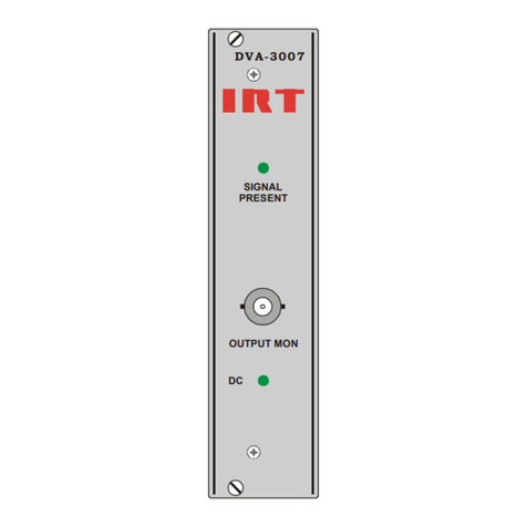
Location
and
Function
of
Controls
instraction
manual.
TA-AV411
Amplifier
SYSTEM
POWER
switch
When
the
SYSTEM
POWER
switch
is
turned
ON,
the
settings
on
the
display
panel
are
automatically
reset
the
original
setting.
SPEAKERS
selector
INPUT
BALANCE
control
Display
window
[5]
Function
selectors
[6]
BALANCE
control
MASTER
VOLUME
control
DBFB
switch
[9]
Graphic
equalizer
controls
REAR
LEVEL
buttons
SURROUND
MODE
selectors
HEADPHONES
jack
Remote
control
sensor
Remote
Commander
MODE
selector
Selects
the
function
mode
on
the
remote
commander.
1:
To
select
the
function
indicated
in
light
gray
such
as
DECK,
DAT,
CD
player
and
surround
mode
of
amplifier.
2:
To
select
the
functions
indicated
in
blue
such
as
VTR,
LDP
(Laser
disc
player)
and
TV.
Installing
Batteries
CDP/LDP
control
section
The
combined
CD/LD
player
can
be
controlled
with
LDP
position.
>:
Play
i:
Pause
m:
Stop
D
(disc)
SKIP:
Disc
skip
(for
a
CD
player
equipped
with
a
multi-disc
changer)
</>»;
Manual
search
(only
for
LD
player)
</>:
Locates
a
desired
selection.
Amplifier/TV
section
TVMIDEO
button:
Selects
the
input
signal
of
the
TV.
(for
TV)
Program
number
(1
to
0)
and
ENTER
buttons:
Select
the
channel.
(for
TV)
SURROUND
mode
selectors
(for
the
amplifier)
ON/OFF:
Turns
on/off
the
surround
mode.
MODE:
Selects
the
surround
mode.
FUNCTION
selectors:
Select
an
input
source
of
the
amplifier.
(for
the
amplifier)
REAR
VOL
/TV
VOL
+/-
buttons:
Control
the
volume
of
rear
speakers
(surround
level)
or
TV.
DBFB
button:
Turns
on/off
the
DBFB
(Dynamic
Bass
Feed
Back).
(for
the
amplifier)
MASTER
VOL
+/—
buttons:
Control
the
amplifier
volume.
(for
the
amplifier)
Tuner/TV
section
SHIFT
and
TUNER
PRESET/
TV
CH
(channel)
+/-
buttons:
Select
a
preset
channel
of
the
tuner
or
a
channel
of
the
TV.
Tape
deck/VCR
control
section
DECK/VTR
selector
DECK
A,B,
and
DAT:
Selects
A,B,
or
DAT
deck.
VTR
1,
2,
and
3:
Selects
VCR
type.
(1:
Betamax
VCRs,
2:
8
mm
VCRs,
3:
VHS
VCRs)
ll:
Pause
m:
Stop
<</>~:
Fast
winding
</>:
Play
@
(REC):
Recording
ANT
(antenna)
TV/VTR
button:
Selects
the
output
signal
from
the
antenna
terminal
on
the
VCR,
either
a
TV
signal
or
VCR
programs.
VTR
CH
(channel)
+/-
buttons:
Select
channel
on
the
VCR.
Power
control
section
SYSTEM
OFF
button:
Turns
off
the
power
of
the
whole
system:
LDP,
VTR,
TV,
and
AUDIO.
LDP/VTRIVVTR2NVTR3/TV/AUDIO
POWER
buttons:
Control
the
power
of
each
unit.
(The
VTR
button
can
be
operative
only

TA-AV411
"S}]alINO
Dy
ssay}
0]
JUsUdInbe
abeyem
yBiy
seujo
sO
AL
‘uey
‘UO
D]O9|8
Ue
Se
yons
saoueyjdde
swioy
jeouj9a]9
Aue
JOsUUOD
JOU
Og
NOILNVYS
“YOUMS
YAMOd
out
Aq
pajjosjuod
ave
sjajino
esau]
;
“SIBNO
OV
oUt
uo
payesipul
abeyem
ay}
vey}
Ss9aj
S$!
UoNdwinsuos
Jamod
asoum
sjuauodwos
oipne
Jamod
0}
asey)
esp)
(ASHOLIMS)
SLATLNO
OV
©
se
Sts
‘yanino
[em
e
0}
JoaUUOD
pio
1aM0d
©
Ce
eae
Seg
ae
hte
Win
packard
ite
*JONUOD
BjoLUa
Wa}sAs
OIDNe
QJIOUM
JO}
P109
jOsUOD
a]OUWd
Je]j
OY}
YW
JUaWdiINbs
Auog
saujo
jo
y9e!
NI
S
TOULNOD
ay)
0}
2auUOD
(payddns
jou)
pao
joz}u09
ajows
jely
@
i
‘jaued
JUOJ}
SY}
UO
JO}OSjas
OU}
UM
Ajsnosueynus
so
Ayenpiaipul
payoajes
eq
ued
Adu,
“g
wajshs
pue
vy
wa}sds
:swaishs
seyeeds
Jo
sured
Om]
JOSUUOD
UBD
NOA
rt
Fa
“punos
punouns
Burholua
10)
suajss
seyeads
128)
jo
ied
e
joauUOD
;
20H
@
Am
Sa
rou
Be
feteckes
eA
es
Siva
ear
OR
Ga
nr
ere
ay
sues
es
peter
z
x
Bnid
cuoyd
—
|
x
Bnyd
ouoyd
Z220-4H
z
x
Gnid
ouoyd
—
5
x
Bnd
tui
SOLD-MuY
es
10P10081
SCe}
OAPIA
[BINEUOLW
104
z
x
Snid
ouoyd
-
z
x
Bnid
oucyd
J9P1JO991
Bde}
OSPIA
CAlS]s
104
"saiqed
Butmoyjo}
8)
8sn
439p1092a4
ade}
Oapla
&
JIQUUGD
OF
‘saniiqedes
Buypuey
semod
ayenbepe
yim
wayshs
Jexeeds
2
9SN
O}
ANS
ag
“SWUYO
91
O01
g
WOW
BoUepEdW!
yeUIWOU
Jo
suayesds
YM
Iseq
410M
0}
paubisap
si
Jayydwe
siyy
Ayoedea
samod
pue
equepaduyy
Jayeads
uo
aj0N
oo
bars
1
es
F
oe
isi:
:
Oo]
ro)
a
\
1
HOA
saAeid
qd
ie)
LNO
OIGNY
9}
4MO
3NI1
0}
~-=
—,
1
a
i
gc
e
eeoe
|
cae
Boal
>
Lad
JeUnL
INO
ANITO
NIS
TOULNOS
OF
indo
935
AdVL
NI
3dVL
INO
S
TOYLNOD
on
NI
ONOHd
“NEGO
LL
PAY
Ni
OJGIA
HaNVadS
LNOHS
°
NI
ANAL
TENT
EFER
TEN
Lno
NI
Dol
INIT
OLE
T
SANIT
O}
=
=>)
Fo
SS
=
i=3
U
Walsks
siqe}uIN,
wT
wb
siayeods
seay
«OP
SHESSEO
eT
5
140in
‘wes6eip
Buyosuu09
SIOYEOCS
JUOIS
JENPIAIpU!
aU}
0]
PUOdSadJ09
@
Paquosep
siequuNu
Bu
‘Maanoedsear
Jaiyduue
ayy
jo
sjeulse}
—
Pue
+
dy}
0]
Pa]DsUUOd
AjjoaUOD
eq
Pinoys
swAa}sAs
Jeyeads
Sy}
jO
SPsOO
—
puke
+
9UL
‘asiou
pue
winy
asneo
Aew
UONauUUOD
aso]
Y
‘syoe!
au;
OU
Payasur
AlN}
aq
P|NoYs
SioJQ@UUOD
B1qeo
Sy}
-(J)
|euUeYS
19}
Bu]
40)
SOU
SYM
PUe
(4)
JaUUeYS
JYGu
JO)
are
syoe!
pue
snd
pay
‘papod
10joo
ae
syoel
pue
shnid
puog
"YO
Si
zaMmod
ans
ayeyy
Ise]
P4100
aMod
Oy
ay}
JOaULOD
suolHQaUuUOD

TA-
AV411
“AWWNSSI
JIM
JO9}jJS
PUNOUNS
JNOYWM
PUNOS
;eWOU
ey
(,03)J8
punowiNs
8|Qesip
04)
44O
“PUNOS
[BINEUOW
O}
199jj9
OBJ]
S]eINWIS
B
SBAID
(punowng
payeinwis)
GALVINWIS
ye
W9OUOd
B
Ul
PSONPOl
SI
yey
JO9jJe
UONEIAQISASL
ne
(punoung
|f@H)
TWH
“J9]B9y}
SIAOW
&
UF
}1.0]
Buruayst]
ayy}
snl
punos
spuedx
3
(puno.ing
Aqiog)
Ag10d
sapow
punodns
Buyjsajas
“(yesnBUOW
$I
PUNOS
BY]
8484M)
UOESJBAUOD
JO
BUaOS
By)
BuNp
peziuuiuiy
S|
Jeyeeds
PuNONS
au)
JO
SWNIOA
(IPN)
au}
yey)
OS
}ONUOD
SIU]
snipe
EPO
GNNOYHNS
AGIOG
uy)
UI
1013U09
FONV1VE8
LONI
84)
Bunsnipy
“pajoajas
S|
SepOW
PuUNOINS
ay)
JO
aUO
ssajun
'sieyeeds
punouins
ay)
Wo.
pseay
eq
jm
PuNos
ON
aJON
AONVIVE
LNdN!
omelt
hey
eouRyue
O]
NO
<—
YSMOd
W3LSAS
Ct]
pe
sims
2
T3A51
YV3Y
gyenusye
OL
‘jeued
Je9J
BU}
UO
S/EUIWIE}
HIYV3dS
GNNOXUYNS
eu)
0}
Pa}deUUOD
ase
(feUdNdO)
ssayeads
Punousns
UayM
BAOa}ja
aq
|JIM
PUNOS
PuNOUNs
aU,
‘J@Ae}
punos
Jeed
‘OSQIA
sseid
‘wesBoud
punos
o=pin
e
104
‘Adv
sseud
‘wes6od
ade)
e
Jo4
‘Og
ssaud
‘weisBoid
qo
&
Jo4
“YANN
SSezd
‘wesGod
Jaun)
eB
104
‘ONOHd
ssaJd
‘wesBoid
piodas
&
104
aounos
wesGold
ay)
Bunoajes
AEG
TET
TRE
FASE
eta
Sent
Es
soe
SF
gs
Fe
he
oa
7%
4
dis
WSLSAS
me
uw
fe}
tg
suanvads
ax
Att
ag
%
3WMONISLSVN
‘wajshs
sayeeds
oy}
198;8S
iG
:
i,
[AQ]
StUN|OA
eu)
IsNipy
G
®
-gounos
wesBosd
ay)
Aeld
v
‘syoe!
3dgV
1
Sy}
0)
payoauuoS
yoap
edej
e
Buisn
aounos
wesGod
Aue
piooes
uRO
NO,
Huipsoo0y
“auoudpeey
ay}
Woy
pseey
jou
ae
sueyeeds
(punouins)
Jedd
JO
PUNOS
aU]
e
‘pueay
oq
UBD
PUNOS
OU
‘AaSIMUaYIO
“"Pa]O@auUOd
9q
ysNW
SLUS)SAS
Jeyeads
jo
sued
OM)
‘g
+
V,
01
19S
SI
SHAMWAdS
USUM
&
Sa}ON
‘dIO.
01
SUINVAdS
18S
‘AjUO
Huluaysy)
euoydpeay
Joy
‘G+
V,
0}
SHINV3dS
Jas
‘ssayeads
YO
BAUP
OL
*G.
©)
SHANVWAdS
18S
‘g
Walshs
Jayeods
BAP
OL
“WW.
O}
SHINV3dS
18S
‘Vv
Waishs
Jeyeeds
OALIP
OL
wajsAs
sayeads
ay}
Bunoajas
OEP
CBPIA
yoap
ade,
JOSURS
JOJJUOD
BOW
SY

TA-AV411
|
SECTION
2
DIAGRAMS
2-1.Description
on
1C101
(yu
PD75206-717-
3BE)
1/0
See
Pim
|
Por
ACT
os
DRLC
SW
A
1
RESET
MH
oa
a
3
=e
315
vs
a
Bi)
Be
m
|
es
$s
| 3
a
oO
ot
jee]
se
09
7
—
ae
he
ww
BG
ct
Comal
ot
ot
ot
oq
a
—
bo
t10
—
oo
ot
—
i
5
is
tl
&
i="
&
om
Te
[vee
[en
SEG9
SEG8
ar
sneraes
Pas
[oe
|e
|
:
paar
n
co
F
a
iW)
CO ~
Pyperpeyeye
om
ga
|
da
=
eg
0
mh
n
nN
(ee)
n
NO}
bd
Oo
|
oO
Vop
do
oo
Ww
N
iS)
o
“
n n
bho
©
wn
n
A
wi
ow
NOs
es
pol
-|-
High
:
High
—
impedance
status
In
:
Input
status

Pin
a
_
[
I
pll
I
(ey
Q
v8)
=
|
to
pl2
n
DRLC
SW
38
pl3
POWER
SW
39
p20
a}
w
Oo}
Oo
(Se)
2
ST
LV1001M
ANS
ue)
—
|
ST
LC7535,/LC7822
4
p22
In
SV
MSM59371
p30
p3l
p32
p33
slelelele
3
3
S
iS
o
>
|
ct
Yn
tH
NS
as)
cs
fe)
i
Q
2
3
a)
AS
Oo
iN
OD
=
DD
47
=
x
foe
[io
fs
|
=
|
1
[recom
sew
z
=
;
-
Q
Ct
(eo)
OQ
|
=
rf
lr
ma)
o
a)
>
S|
2
Alle
~
ao)
®
>"
<
te
oO
oo
p42
p43
on
oi
oO
iw)
e
57
58
N
<
pS
-
a
on
co
xtl
50
pol
p52
p53
|
to)
DRLC
READY
MIX
SW
DOLBY
SW
oO)
iS)
(op)
(oe)
oral
3
B
Oo)
as
High
:
High-impedance
status
In
:
Input
status
|
TA-AV411

TA-AV411
|
2-2.
Key
operation
(7)
SIM
PORT
Key
input
has
priority
over
serial
input.
The
port
is
turned
to
”L”
when
SIM
is
selected.
(Key
input,
Serial
input)
Note
1.
SURROUND
ON/OFF.
(1)
Setting
(2)
FUNCTION
Key
(PHONO,TUNER,
CD,
TAPE,
VIDEO1-4)
operation
These
keys
execute
operations
below
when
pressed.
FUNCTION
IC
-+++:++-
Serial
data
REC
OUT
SW-:::::s::
Static
data
VIDEO
SW:seeeeeeeeces
Static
data
FRONT
MUTE:::::°:::
One
shot
REAR
MUTE
:::::::+::
One
shot
(3)
REAR
MUTE
PORT
The
port
is
turned
to
”H”
by
switching
to
SURR
ON,
MODE
or
FUNCTION.
(Key
input,
Serial
input)
Also
the
port
is
”"H”
three
seconds
after
POWER
ON
is
selected.
REAR
MUTE
PORT
has
priority
over
other
ports
to
output
when
POWER
OFF
is
selected
and
operates
when
SUB
VOLUME
is
turned
to
~.
However
there
is
no
output
for
the
port
switching
the
main
FUNC
TION
when
DRLC
ON
is
selected.
(4)
DRLC
CONTROL
PORT
(used
for
SP
relay
too)
The
port
is
turned
to
”H”
only
when
DRLC
ON
is
selected.
(Key
input,
Serial
input)
(5)
POWER
RELAY
PORT
The
port
is
turned
to
”H”
when
either
POWER
ON
or
DRLC
ON
is
selected.
(Key
input,
Serial
input
RM-1,
-RM-2)
Both
MAIN
and
SUB
are
turned
OFF
when
ALL
OFF
serial
input
is
selected.
(6)
DOLBY
PORT
The
port
is
turned
to
"L”
HALL
or
SIM
is
selected.
(Key
input,
Serial
input)

The
relation
between
Switch
ON
and
FUNCTION
Sw
A-AX311/AVA411
1,
PHONO
10000001
2.
TUNER
01000001
3.
CD
00100001
4,
TAPE
00010000
5.
VIDEO
3
none
6.
VIDEO
2
7.
VIDEO
1
8.
VIDEO
4
Serial
data
to
SURR
IC
(LV1001M)
The
delay
time
is
controlled
with
8-bit
data
(short
mode).
The
delay
time
is
decided
by
the
count
time.
(Address
data)
-
FFFF
(short
mode)
none
00000011
none
15mS
*+++++%%
8ABOh
20mS
++eerers
63C0h
SOmS
«++++re-
15A0h
Timing
chart
VOL+/-
RM-~-1
The
operation
is
carried
out
in
100mS
even
though
the
data
fin
ishes
2
frames.
VOL
——_
MIN100mS
MUTE
must
be
switched
100mS
forward
or
backward
during
SURR
MODE
switching
(including
SURR/OFF
switch).
SURR
'
100mS_
:
100mS
MUTE
FRONT/REAR
Port
FL
SUB
VOL

|
TA-
AV411
POWER
ON
(The
same
operation
when
starting
the
buck
up
system.)
POWER
ON
MUTE
FRONT/REAR
POWER
RELAY
The
data
for
SUB
VOL
is
©
when
DRLC
or
SURR
is
turned
OFF.
500mS
DATA
DISPLAY
POWER
OFF
POWER
OFF
MUTE
FRONT/REAR
!
;
100mS
POWER
RY
All
the
light-off
data
FL
DATA
OUTPUT
PORT
The
last
status
—10—

TA-
AV411
DRLC<—SURR
mutual
switching
DRLC/SURR
7
ON
|
:
|
MUTE
FRONT/REAR
Poy
t0Oms
ts
Output
port
FL
tube
data
SUB
VOL
DELAY
TINE
(only
for
SURR
ON
Display
operation
1.
FL
tube
start
timing
92
us
i
100
ws
dig
1
dig
2
dig
3
dig
4
dig
5
dig
6
dig
7
seg
50
us
a
|
ee

2-3.
MATRIX
for
FL
tube
and
KEY
IN
KEY
IN
10
aes
FT
CT
eae
ae
See
NA
A
A
A
seg
10
seg
2
O
seg
3
O
seg
4O
eerste
eae
a
ee
oe
ae
ceed
aes
iene
(ae
ea
a
seg
9
O
deg
20
oo
pine
ae
ce
ee
ey
deg
50
deg
6O
ees
=
ae
ee
ee
os
deg
9O
Key
scan
operation
@
Key
input
has
priority
over
serial
input.
@
If
a
key
is
input
10mS
after
the
same
key
was
input,
this
is
recognized
as
a
key
input
and
registers
five
times.
@®
Double-pressing
is
not
accepted,
one
pressing
first
and
being
replaced
by
a
second
has
priority.
@
No
keys
can
be
input
during
POWER
OFF.
©
No
keys
can
be
input
for
1
Second
after
POWER
ON.
Key
scan
operation
Key
in
p
50
|
|
Key
in
p
51
|
|
Key
in
p
52
|
|
Key
in
p
53
|
Key
scan
10mS
Bes,
|e
a

Timing
chart
DRLC
DRLC
SW
REAR
MUTE
|
|
:
100mS
DRLC
CONTROL
POWER
RELAY
|
DRLC
display
on
FL
tube
data
SUB
VOL
data
DRLC
FUNCTION
FUNCTION
switch
Serial
data
REAR
MUTE
!
100mS
DRLC
FUNC
|
A+B
3
|
100mS
B83:

2-4.Description
on
IC303
(LV1001M)
Explanations
De-couple
capacitor
for
threshold
voltage
Capacitor
for
smoothing
of
rectifier
output
Capacitor
for
sliding
band
filter
and
Delayed
output
Capacitor
for
sliding
band
filter
Capacitor
for
pre-emphasis
Input
filter
for
rectifier
Input
filter
for
rectifier
Reference
voltage
Reference
voltage
Mute
control
Vcc
Output
for
Vpp
Clock
input
for
serial
input,
data
input
for
parallel
input
mode
Data
input
for
serial
input,
data
input
for
parallel
input
mode
Column
address
selection
for
serial
input,
data
input
for
parallel
input
mode
Row
address
selection
for
serial
input,
data
input
for
parallel
input
mode
Connection
to
memory
device
Vss
X’tal
resonator
for
oscillator
X’tal
resonator
for
oscillator
Long
or
Short
mode
selection
Serial
or
Parallal
mode
selection
For
test
mode
Smoothing
for
NR
rectifier
Smoothing
for
NR
rectifier
Capacitor
for
weighting
on
side
chain
path
Input
for
variable
resistor
NR
output
7kHz
low
pass
filter
output
Input
for
NR
Capacitor
for
de-couple
on
NR
Delay
output
or
NR
output
Input
for
mute
circuit
Output
for
mute
circuit
Output
for
7kHz
low
pass
filter
Input
for
7kHz
low
pass
filter
GND
Input
for
right
channel
Input
for
left
channel
Capacitor
for
de-couple
on
Fixed
matrix
output
Noise
shaping
and
delay
input
Noise
shaping
output
Delay
input
signal
mode
select
switch
(L+R/L-—R)
Filter
for
supply
voltage
on
comparator
Capacitor
for
sliding
band
filter
and
local
decoder
output
=)

Input
Address
Port
Timing
SHORT
MODE
MSB
LSB
tSTH
SRAS
SCAC
*
wa
In
case
of
short
mode,
delay
time
setting
is
set
in
above
timing.
The
date
loaded
to
SDATA
is
written
on
the
leading
edge
timing.
In
order
to
select
that
the
data
latch
for
row
address
strobe
or
column
address
strobe
is
loaded,
SRAS
or
SCAS
port
is
controlled.
When
changing
delay
time
setting,
meaningless
data
on
a
memory
are
read.
this
causes
the
pop
noise.
when
SRAS
or
SCAS
is
controlled,
mute
circuit
(pin
55
is
input,
pin
56
is
output)
is
activated.
Mute
time
is
the
same
as
the
delay
time
which
is
set
at
that
time.
(Serial
data
input
mode
only,
On
parallel
data
input
mode,
mute
circuit
is
activated
by
using
the
mute
control
port
pin
18.)
On
long
mode,
input
data
number
is
9,
the
way
of
setting
delay
time
is
same.
—15—

2-5.
CIRCUIT
BOARDS
LOCATION
FUSE
BOARD
SP/TM
BOARD
CN
BOARD
SP/SW
BOARD
SURR
BOARD
HP
JOINT
BOARD
SURR
JOINT
BOARD
SURR-SP
BOARD
HP
BOARD
AMP-R
BOARD
MAIN
BOARD
VOL
JOINT
BOARD
VOL
BOARD
DBFB
BOARD
CONT
BOARD
4
AMP-L
BOARD
4G
2-6.
SEMICONDUCTOR
LEAD
LAYOUTS
CXA1100P
CXA1198AP
M5226P
TC4051BPHB
16
9
ae
8
1
(TOP
VIEW)
M5F7805L
M5F7812L
M5F7912L
COMMON
(GND)
in
OUT
Piguts
8
LA3160
M5128AL
yu
PC1237HA
12345678
LC4966
MC14066BCP
TC4001BP
yu
PD4011BC
14
8
i
ckee!
J
T
(TOP
VIEW)
»
PD75206GF
-
717-3BE
(TOP
VIEW)
LCG7822
(TOP
VIEW)
IRZE31A
123456789
LB1639
Gai
SI-
18752N
x
2SA1175-HFE
2S8C2785-HFE
LETTER
SIDE
DTA124ES
DTA144ES
DTC114ES
DTC124ES
DTC144ES
2SC2603-
FE
Ec,
2SK246-Y
SGD
2SA733-
QP
2SC945-QP
2SC1815-Y
2SC2682-
QPE
LETTER
SIDE
47s:
TA-
AV411
2SA1684-LK
2804431-LK
2S8D2012
:
HZS6C3L
HZS6C2L
HZS30-1L
;
Cathode
Anode
10E2N
181585
Cathode
Anode
RBA-
402
RBV-602-01
+
ww
SEL2210S-CD

TA-AV411
9
Fg
a
a
(_
2-7.
PRINTED
WIRING
BOARDS
A
ss
=
es
es
aia
sige
*
Semiconductor
Location
[
a
[
ee
Je
=
—_
-—_._
..-"*
[SURR
SP
BOARD
}
H-7
Q405
SURR
H-7
[SP_SW
BOARD]
—
(RX
BOARD
]
JOINT
[
]
ne
8
Patel
BOARD
-7
J-11
BOARD
a
J-11
“an
,
[HP
JOINT
BOARD)
|~
9
o|
—
I-10
B23
:
=
Ans
G-8
|
1-638-286
—
L
a
1-638
-284
[ur]
fii]
1-638-279
W—_
o|
+
C-31
oneal
C-
31
J-28
[11]
K-28
im]
(]
1-25
J
1-24
H-23
is
H-
23
D-
23
[CN
BOARD
]
=
5-28
h
es
AX
a
oa
F
C000
as
a
as
=
IMPEDANCE
USE
AC
i20v_
60H
Ser
[CONT
BOARD]
:
: ‘
es
a
¢
Ae
CNP9OI
‘.
os
i
ee
om
é
pia
|
:
a
de
si
62)
i
ie
7
:
‘
“
die
et
H
th
ri
-
a
:
a
G
an
pe
fm
i
3
J-36
g-3
J-36
I-
36
H-9
|-
36
D-
12
H
J-37
D-19
[DBFB
BOARD)
J
_
36
E-
20
1-638
-287
if
Sl
J-
36
G-21
(eh
Ln
I-
638-273
[1]
=
7
F-
1-6
E-19
|
a
2
os
[
AMP-L
BOARD
]
E-20
H-19
E20
a
|
g
.
[x
Fs
8
E-20
C-19
:
3
E-20
C-
20
:
3
F-
20
D-
32
J
,
H-20
D-23
H-13
D-22
I-12
D-21
[ii]
[RIGHT]
|
SURROUND
MODE
_|
K
L
Note
on
Mounting
Diagram:
|
®
oO-——
:
parts
extracted
from
the
;
1-
638-270
[tt]
component
side.
.
——<
45°67
<6
>
—
18—
—19—
—20—
—21—
—22—

TA-
AV411
2-8.
SCHEMATIC
DIAGRAM
Ue
er
ok
eteata
A
oes
—
2
3
4
5
6
8
9
10
11
12
3.
|
14 15
16
7
18
19
20
21
22
23
24 25
260
27
J502-3
:
F
: : :
TCeOT
ages
CS
oe
eee
ee
ea
eG
eee
ee
ee
rot
1
:
ier
eS
nee
ee
oe
705
2SAT1%2
7
a5
:
.
f
BOARD}
[HP
JOINT
BOARD]
A506
Ik
|
3
E
fi
A
TAPE
IN
=
ue
ene
on
I
ee
wats
er
ee
1.5k
|
M
-
|
neis
i
Ba)
ee
[
seo
WAN
J700
H
=
k
TOKHZ!
>
'
‘
[PHONES]
ee
R5Oe
Tk
:
|
;
4
+
:
4
+
RV405
1
oy
CAB
x
!
oe
67.5
ne
apie
a
+
:
AN
Ee
laos
1
.
|
=
EA
C403
.
3
431
751-754
R783
=e
A508
x
+
|
iis
|
|
Sov
r
|
|
Cia]
yi
2
| |
ai
Lay
2
the
DIFF
AMP
360
[HP
BOARD
]
WIBEO_
IN
rn
: :
.
; F
EeTS
'
=
:
‘
cN707
+
ee)
501-3
R502
27k
eis
:
|
1
L
SOV)
cate
|
ee
| |
83
uta
3.3
P-5p.
2sc792
+
|
AA
eN706
:
——_
ISP
TM
BOARD
}
ca_IN
ms
v7
[(c4017]
Fa
ve
a
J501-5
R501
330
Ws
es
R724
L701
|
7
PHONG
_IN
C510
|
1
25hre\er
0402
TONE
CONTROL
AMP
DES
: 1
|
R22
:
'
aos
|?
u
10
0.001
@BFB
SW1TCHING
28C2785
tools
c70)
soe
330
R726
R734
RYZB
ILS
ENDO4)
:
=
y
:
0}
BBFB
SWITCHING
mot
Sy
eee
C705
47
ZV
Geel
y
R720
1/24
o
10
tay
a
ig
Lo
5
C413
s
+
3
1
+
Lk
+
Lot!
L
B>A*OFF
=
A+B
“11.
‘0
So
28
|
Ti
e703"18
os
Ne
ak
{R721
|
8727
|n7a0 c710]
|arze
10
ito
7
F
&
Sov
TY
:
fr
avi
zat
0
g7or
|
27°
|
|RASF
B=
|
Ik
pret!
15k
0.1
i
ty!
ul
Pol To]
R
'
are
:
©
+
10402
‘
iL
“stb
C708
“eg
10
ebb
Tot
£
'
oft
to
2
B
"
&
<
5
Rigi
cabin
SOV
LB1639
| |
R417
702
>
47
tL
i :
Mim
FRONT
SPEAKER
Boe
Ze
BoB
£04,
R409
R410
ao}
|4:7%
=
|220p
R703
f705
|
16V
R718
ahs
+
:
:
of
i
50!
P°S
SESE
g
ji
swt
=
4.7
ayo
2
1.5k
alia
i
a
=
704
om
Soe
ee
Her
a713
SE
|
a4,
Lassoe
:
mi
TOREDANGE,
USE:
TO
CONT
BOARA
1/2
ae
=
a
:
B=
p2sc18
8-160
.
1¢502
167822
‘
|
Réos
-1
$
car
Sb
25h
IBALANGE)
Ss
he
RAPUEEIL-2*
.
8
Fa
2502785
IN4148M]
e-79g
a
PSAl215)
|
BQ
s
maa
|
:
ene
as
—
220
R729.
otto
L
em
sate
poor
RAQS#R408
RAL
ENCOd
Tan
ama
a
|
AI
.500v
TON
ee
ides
iALI#
|
|
Lol
Ho
-
“LIN
ie
B=]
casi
givin
100%
ae
j
ae
R731
i
i
Lo to
2
(N10
CELE
[CONT
BOARD
2/2]
C555
C556
;
FE
—-
:
Se
ee
oe
Oe
ee
a
a
BE,
Sieh
I
5
a
a
1
24
;
le
:
u
My)
[ees
Vee]
o712,
|
a
5
|
PGND
IN
ie
ue
Tes
ros
=A
RIGHT
(Bt
“2
his
ui
Ey
re]
t
|
rol
,
Se
a
B
hak
Ss
R763
oft
-
:
ee’
RSSZ
Ik
*
“Wr
RR?
(roonZ]
(Ssonz]
[KAZ]
SKA]
“2
aa
Sy
i
22
enEGeL
'
1
aL
Lf
|
01-2
RSSS
tk
i
s
RV410
RV451
RV452.-RV453—ORVASS
1k
ae
aN,
IM
S
Bie)
Pate)
Pay
OVER LOAD
BET
|
tL.
—_
-
___
.__.
|
—
BIG
i
lf
TE
Ss
|
:
:
Cc
a
vO
I
Sree
niga
INPUT
4
‘we
KE
Rag
al
R767
es
eae
mex
Ins
46M
|
Note
on
Schematic
Diagram:
TUNER!
BALANCE
[
:
=
'
0
{Ss
’
t
vars
a
HE
i
i i
J502-6
RSS3
10K
N5218AL
7
:
an
es
el
cn4o2!
Po
fe
=
s
R7E9CS/
R774
Is
|
|_0742
SP
BOARD
]
INGT4BM
wy
5Y
@
All
capacitors
are
in
uF
unless
otherwise
noted.
pF:
wuF
REC
UT
Ww
G455
om
usr
3
casa
cue)
t
;
DSheEa3A
j
ele
lliis
|
BR
|
lazesl
eros
10
gX°|
282921
[SURR
JOINT
BOARD]
Balen
“Soo
aL
STOP
106
Lz
ficmoc
ro
a
re
|
ae
]
°
e
ks
a
in
ra
|
Hasek
|
ae
||
‘50V
i
Se
te
MUTING
|
re
STS
ie
OR
||
tk
=
aN
eae
:
tie
NG,
th
hone
a
>
pepe
eee
:
i
SWITCHING
6-5
7
|_|
rl
ES
alls
<5
60
2
0
pee
sel,
aoe
|
S5OWV
or
less
are
not
indicated
except
for
electrolytics
c=)
: :
.
i
iJ
Th53
0.012
|
0.0089
|
0.0012
a
oe
[VOL
BOARD]
|
1
{R72
a
1k
B30.
172W
pad
|
[SURR
BOARD
]
ip
ae
g
=
FLIOI
Sie
ietean
eda
a
101
PHONG]
|
sio2
TUNER!
sigs
(Al
|
stos
[TAPE]
|
sios
(WIBEO)
ft
and
tantalums
;
i '
3
:
B=]
:
~ececocooes:
nee
|
uu
tit
"et
aS
a
aa
r
:
Q
7
TTT
agus
[|
Pas
|
I
ron
|
All
resist
in
2
and
'/,W
or
less
unless
otherwise
'
ae
A4S4eRAsox
Ate
|
AAA
7
'
|
ae
4
p
RII
malts
ro
-
REAR
SPEAKER
4
Wee
3-4
2802785
|p
,
=F
cts
=
Bj
®
resistors
are
in
an
4
ss
s
is
Ms
kaRAS
:
5)
yb
ie
756
|laocl
ok
TT
R777
R780
C760)
FT
Sil
ey
H
TUEReeTaE
(3)
(S1.)
ccd
SWITCHING
C"
t—~o
o—
a
5V
ie
e305)
t——+
u
C75)
R752
33k
oes
4
|
30%
Be
arya)
ON
re
10
ab
603
i]!
=
4.9
OT)
|cio2
pe7t
|
mi
sio3
[4]
suo
El
STOP
)
specified.
1C305
(172)
R451]
R453/C452
8
a
fa)
2.2k
'
1N4148M,
a
Sy
oe
BUFFER
AMP
MSZ1BAL
11g
[B+]
700k!
330
|.
47
+1
1
EA
iy
7
Ree
9754
Z
POWER
AMP
(REAR)
7
(>
4|
0.1
R107
We
[REAR
LEVEL
REAR
LEVEL]
G
J
;
BUFFER
AMP
:
4
moos
SOV
i
G
R759
18
An
US1030
‘yy,
‘14
330
All2e
|S
F
R303
C304
C307
C451
PA)
c
330
'
R775
~
[os
1c40!
+
4.7KT
i
S116
=
cha aha
{IDBFB
BOARD
]
e
:
nonflammable
resistor
10K
16
50V
ig
(8)
4.7
|
|
i
“0.4
a
ae
i”
|e
5
it:
29-4
see
©
ai
Sette)
+9
$0
o
fo
6
.
50V
A
if
:
TN
f
VY}
|
oR
i)
C191
—
[BOLBY]
ACL
S115
:
.
:
D
|
y
a
av
Nat
R413
TO
CONT
BOARD
2/2
+
2802785
4
iy
Zam
si
BE)
ae
2skties
e
oie)
aves
1 t
ceor
pons
»Ge0,.|
L601
;
SEG2
(fo)
fio
yer
4.47
AOS
Ailes
SORROUND
MODE
g113
DOLBY]:
|
5114
IHALL]
STHUCATED
ait
@
fw
:
fusible
resistor.
‘
oo
oe
<
RaSse
'
R760
R761
2502682
’
=.
M0
800008
S
D.22eeer
ven
sees
@)
;
olo}*
mt
oj
-
om
t
|
|
=
R452
58
|
+
220
220
68.1
0763
R779.
—
Ww
secs
(2)
Sa
TTCHING
in
a
am
Fl
Re
2|7/
|
Slol
an,
SORROUND
a
,
“68.1
R746
2SA1215
id
¥
LAF
i
4
i
=
=
MB
Ira
0
'
.
+g:
+
——
ee
2
Cc
‘
sos
(@
Mito
©
4
4
MOaE
Note:
The
components
identified
by
mark
or
dotted
$0
9452
CAIT
R&I
4
8
:
a
it
RIBIF
nop
‘
z
8607 RGO6
DODOOVOOCOGOOOOODO0OO8)
Sle
|
F
.
Ae
iv
|
2sti78s
Lif
sv47e']
oie
"SK
|
aes
:
|
ropa]
Eo
se
|
220
a
|
Ne
S
=
2G
5c
R
eos
mle
se
1s
1
OB
line
with
mark
are
critical
for
safety.
J
Ol
og:
|
(as.
ae
ee
en
me:
A
Té0V
pom
I
sees
(Q)
—
SaE
«cli
insteam|
=
1NeteM
a
Replace
only
with
part
number
specified.
aii
Q451
2SK246YGR-TPEZ
T@454]
Tone
cotrou
av
:
[
AMP-R
BOARD
]
nga
|
=
secs
(@)
|
G@)
v2
a5
=
2
&
B105
*
k
«&
x
5
__DBFB
SWITCHING
_
.
j
180
*
=|
Fé04
céo7/_%
|
=|
|Reos
@)
vsr
Sy
eet
ini
N41
48M
sir
109
-
'
SWITCHING
TE
ES
Bo
Ny
eh
ee
hg
ee
ee
ee
ee
|
Reo!
5
bids
£608
os
ed
Ss
10
——
es
(54)
POWER/RY
KEY
SEG1
ea
1N4148M
ie
e
:
B+
Line
7
a
(cao)
“=
|
BS
oS)
-R/SP/RY
23.5
i
C403
=
[C101]
2.
+2
:
4
ms
cN2
|
2
ey
aLsov
Rega
Re10
|
a
a
xi
SYSTEM
CONTROL
3
3@—71]
bd
:
B—
Line
u
a
.
a
(ee
:
j
x2
:
-
FA
|
es
OD
eas
Os
no
mark:
No-signalPHONO
MODE
26
k
-717~
:
‘
F
E
ace
VC707)
'
a
x1
Or
©
Voltages
are
taken
with
a
VOM
(input
impedance
10M
Q)
Q715
1C701
46
x101
xT2
(24)—
i
ae
:
B=]
DSCSBUSKTP-LK
uN
pPCIZSTHA
Z
wis
|
28
;
ORLC/READY
onan
Voltage
variations
may
be
noted
due
to
normal
produc-
Nw
&
5V
MUTING
a
2SC2785
'
MIX/SW
(22)
4
.
46
ehecae
Sr
|
RELAY
DRIVE
aes
;
Satay
P
27
tion
tolerances.
[e403
103
4
7
:
|
ae
a7
hy
740
=
oy
ENeO!
sss
7
Rie
#
@
Waveforms
are
taken
with
a
oscilloscope.
:
a
a
eS
te
ees
Zaz
S52
3322
=
2
RI
er
=z
=
X7S7<
Py,
19
|
R736
56k
|
ata
2
be
als
&
S|
ays
47K
Voltage
variations
may
be
noted
due
to
normal
produc-
|
“Ke
+
||
Den?
$08
:
z
|
*
|=
lage
Ss
tion
tolerances.
1
16ve
mye
oe
=
7
|
E23,
=
47,
INKTABN
9738
|
=
@
Circled
numbers
refer
to
waveforms.
F
l
cris
RRAl
C71
:
=e
Signal
path.
pe
ee
100
|
$.3V
aey
|
c>
:
PHONO
!
ieee
gf
QOLBY
SURROUND
|
4g
a
[CN
BOARD
]
c
7
(1€951]
1707
|
R35
C353
CNY:
3.8
toe
PASSIVE
BECOAER
iesstl
usiogo
Yow
1
;
hy
SB
sv
a
ay
“Hy!
RAS
-
aes
ass?
icast
“FB”
p9s7
B+
fags;
6°31
fh
eee
=
&
|
tart
a
SO
ara
[Mts
sao
a
ve:
22
7805
SOV
UZL=27
ross
nv-to2
ov
BY
|e
|
1901
AS
a
eae
a
A
r
+5V
190d0
Fa
6
10
e352)
aah
a
7
2.2
:
aii
al
pel
cae!
tL
Tv
;
5
1
po
bipeies
tee
mnie)
ODEOROT
=
C314
3.7
241
|
al
°H65
1g
les
16301
(2/2)
1302
a
'30p-l3
76
24
=
ey
R956]
ROSS
aL
6954
ie
Z|
c952
M5218AL
L4966
-11.9
|-|
|
pOtOR,
6.1
ane
re
5.6k|
220
Ee
gogo
)
6.01
1
G
16301
9302
0304
BNIFAH
é
21
it
is
|
2
+
[315A
:
BUFFER:
ANP
BNIF4M
11.9
ee
7
ae
on
TCg52
ie
A
ig
TO
CONT
BOARD
1/2
w
Ad
5
.
|
or
ae
=
5
|
RISE
2.2
1C952
7812
ae
saoossy
NL
ST
ah
A
W.9
1t.9
-
!
m
4317
Bano
iS
EI
Tt
1
a
959
+
955
ed
Fae
F
shy
Rais
6
9307
R/SP/RY
R426
100K
T
2
2200
foe?
19953
L
cose
R/RY|
MIX}
SIM
a
.
2512012
5v
10E2
7
0.022
_—_-—:-
Oho?
—-
-
“3p308
R323
=
OOOO
OD
OOM
DOO
AD
REG
£945
0960 ROS?
9954
9953.
0301
71
47k
“7k
ai
q
Tin
4
4°77
70004
£954
957
.
AN;
td
2SAT175 2802785
£958
5
;
OFF;
LC YL
|
Lt
|
patram
9.0
stl
Lo]
cas
|
ye
<|s|
ey
=27N
7
25V
oe
T
9567
10E2
J0-022
LA]
9952
‘Qf
AC
OFF
QETEGT
RELAY
aR)
a9s2
sales
Ava0t
S|]
1505
R/MUTE
4K
1 :
‘
2802012
|
PY
Ce)
athe
~
a,
fois]
"ual
TTT
BP
en
1H
wie
_
Aa
|
i
A
IC502
LC7822
IC701
»
PC1237HA
HALL
|
H
|
HW
|
OL
BAIFAM
aso1-as0g
A729
c330
aly
0337
C338
:
ay
a
=
=
‘
Birney
0329
4f
R345
SY]
35
AAA
GY
—
4h0336
aL
320
fcss3
470
{Md
270
a :
H
s.stT[H
|
H
|
H
Dohe
SH
TTCRING
:
bv
T
PEF
soy
OT
Ey
oye
ivan)
T&S
REE
cNSO}
CNPSO!
|
MIX
+
J
|
A
1.
SIM
1
I
io
a
ee
ee
=
eg
Ee
i
pe
St
a
fe
ge
ee
a
ee
kg
a957_
956
955
1902
‘
25C2785
2SATI75
2502785
!
965
=e
SWITCHING
AC
GFF
DETECT
J
ares
Ss
ef
NN
er
emer
[
FUSE
BOARD]
QO
LATCH
/
R
5d8
OUT
R
1dB
IN
R
1d8
OUT
AUTORESET
IC404
LC7535
OUT
2-9.
IC
BLOCK
DIAGRAMS
IC302
LC4966
IC402
LB1639
|
sW_D
swe
OR
Va
VDD
CONTA
CONT
B
IN/OUT
OUT/IN.
OUT/IN
IN/OUT
OUT2
VCC
OT
ee
Fe
ALTOS
ee
eS
it
sh
itn)
Ste
pee
a
edt
cali,
NN
GAS
ee
oe
ee
pore
ly
|
[ewe
eae
DRIVE
CIRCUIT
aa
es
vss
IN‘4
GND
V
CONT
IN2
CONTROL
.
"6
VY
a
|
Xx
£\
ES
LS
LVN
IN/OUT
OUT/IN
OUT/IN
IN/OUT
CONT
B
CONT
C
Se
mae)
ae
SoA
SW
A
Sw
B

TA-
AV411
SECTION
3
EXPLODED
VIEWS
NOTE:
e
-
XX,
—X
mean
standardized
parts,
Items
marked
“x”
are
not
stocked
so
they
may
have
some
differences
from
the
original
one.
®
Color
indication
of
Appearance
Parts
since
they
are
seldom
required
for
routine
service.
Some
delay
should
be
anticipated
when
ordering
these
items.
The
components
identified
by
mark
or
dotted
line
with
mark
A\
are
critical
for
safety.
Replace
only
with
part
number
Example
:
The
mechanical
parts
with
no
reference
specified.
KNOB,
BALANCE
(WHITE)...
CRED)
number
in
the
exploded
views
are
not
t
t
supplied.
,
Parts
color
Cabinet's
color
Hardware
(#
mark)
list
is
given
in
the
3-1.
OVERALL
SECTION
1
not
supplied
Ref.
No.
Part
No.
last
of
this
parts
list.
‘not
|
supplied
Descriptiion
Remark
Ref.
No.
Part
No.
Descriptiion
Remark
1
3-350-426-01
SPRING,
RING
13
1-590-538-11
WIRE,
FLAT TYPE
(7
CORE)
2
4-943-091-01
KNOB
(VOL)
14
1-590-485-11
WIRE,
FLAT
TYPE
(7
CORE)
3
4-943-092-01
PLATECVOL),
LIGHT
GUIDE
15
*
A-4341-682-A
CONT
BOARD,
COMPLETE
4
4-943-420-01
KNOB
(DIA.
19)
16
*
4-943-107-01
HOLDER
(FL
TUBE)
5
1-590-486-11
WIRE,
FLAT TYPE
(7
CORE)
17
*
4-921-941-01
CUSHION
(FL)
6
1-590-487-11
WIRE,
FLAT
TYPE
(17
CORE)
18
A-4323-854-A
|
PANEL
ASSY,
FRONT
T
4-928-635-01
SCREW,
+BV
(2.
6X8)
TAPPING
18
*
1-638-279-11
VOL
JOINT
BOARD
8
3-704-366-01
SCREW
(CASE)
(M3X8)
20
*
1-638-278-11
VOL
BOARD
9
4-931-031-11
CASE
21
*
1-638-277-11
RX
BOARD
10
3-706-165-00
SCREW
22
*
1-638-280-11
|
DBFB
BOARD
11
*
4-943-458-01
PANEL,
BACK
23
*
1-638-284-11
SP
SW
BOARD
12
X-4941-229-1
FOOT
ASSY
(F2112S-M)
24
*
1-638-285-11
HP
BOARD
25
*
1-638-286-11
HP
JOINT BOARD
97
=

3-2.
OVERALL
SECTION
2
CNP901
line
with
mark
are
critical
for
safety.
Note:
The
wth
mark
are
ert
by
mark
A
or
dotted
part
number
specified.
Replace
only
wit
Ref.
No.
Part
No.
Descriptiion
Remark
Ref.
No.
Part
No.
Descriptiion
Remark
51
4-885-901-31
SHEET,
RADIATION
60
*
1-638-271-11
|
AMP-L
BOARD
52
1-533-217-31
HOLDER,
FUSE
61
*
1-638-281-11
|
SURR
SP
BOARD
53
*
A-4341-678-A
MAIN
BOARD,
COMPLETE
CNP901
/A\1-551-478-00
CORD,
POWER
54
*
3-703-244-00
BUSHING
(2104),
CORD
F901
A\1-532-749-11
FUSE,
GLASS
TUBE(6A)
55
%
1-638-273-11
CN
BOARD
F951
”\1-576-107-11
|
FUSE(3.15
A)
56
*
1-638-276-11
FUSE
BOARD
F952.
A\1-576-107-11
FUSE
(3.15
A)
57
*
1-638-282-11
|
SURR
BOARD
(
A
including)
T7901
A\1-450-370-11
|
TRANSFORMER,
POWER
58
*
1-638-287-11
SP, TM,
BOARD
59
*
1-638-272-11
|
AMP-R
BOARD
L9G...
Other manuals for TA-AV411
2
Table of contents
Other Sony Amplifier manuals

Sony
Sony XM-GTX6021 Installation instructions manual

Sony
Sony XM-460GTX Marketing Specifications User manual

Sony
Sony XM-2020 User manual

Sony
Sony UDA-1 Operating instructions

Sony
Sony TA-F448EB User manual

Sony
Sony XM-280GTX Marketing Specifications User manual

Sony
Sony TA-P9000ES - Amplifier User guide

Sony
Sony TA-EX66 User manual

Sony
Sony TA-AX390 User manual

Sony
Sony XM-D9001GTR User manual