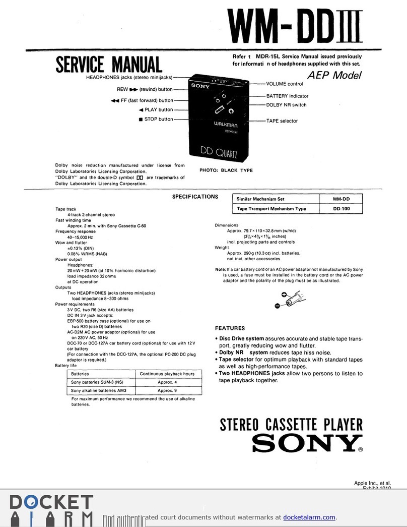
Sony TC-SD1 User manual

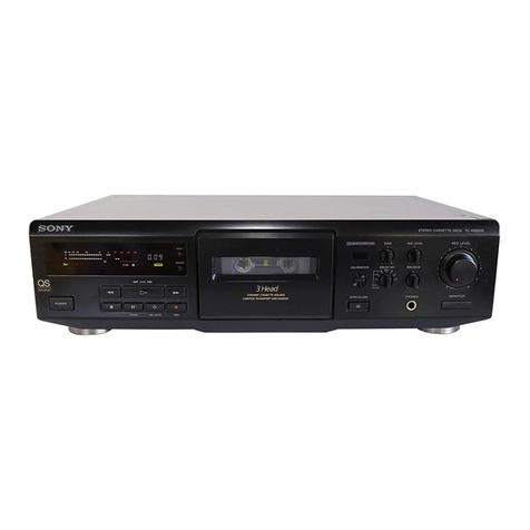
TC-SD1
AEP Model
UK Model
E Model
SERVICE MANUAL
STEREO CASSETTE DECK
MICROFILM
ManufacturedunderlicensefromDolbyLaboratories
Licensing Corporation.
“DOLBY”andthedouble-Dsymbolaaretrademarks
of Dolby Laboratories Licensing Corporation.
Model Name Using Similar Mechanism TC-PX100
Tape Transport Mechanism Type TCM-ACLM572
SPECIFICATIONS

— 2 —
SAFETY-RELATED COMPONENT WARNING!!
COMPONENTS IDENTIFIED BY MARK !OR DOTTED LINEWITH
MARK !ON THE SCHEMATIC DIAGRAMS AND IN THE PARTS
LIST ARE CRITICAL TO SAFE OPERATION. REPLACE THESE
COMPONENTS WITH SONY PARTS WHOSE PART NUMBERS
APPEAR AS SHOWN IN THIS MANUAL OR IN SUPPLEMENTS
PUBLISHED BY SONY.
TABLE OF CONTENTS
1. GENERAL ·········································································· 3
2. DISASSEMBLY
2-1. Case, Front Panel································································ 4
2-2. Mechanism Deck (TCM-ACLM572)································· 5
2-3. Control Board, Dolby Board ·············································· 5
2-4. Power Trans Board, AC Select SW Board, Power Board··· 6
2-5. Tray Assembly ···································································· 6
2-6. Mechanism Chassis Block·················································· 7
2-7. Capstan Reel Motor (M902)··············································· 7
3. DIAGRAMS
3-1. Circuit Boards Location ·····················································8
3-2. Schematic diagram — Display Section —························· 9
3-3. Printed Wiring Board — Display Section — ··················· 11
3-4. Printed Wiring Board — Main Section — ······················· 16
3-5. Schematic Diagram — Main Section — ·························· 21
3-6. IC Block Diagrams ··························································· 25
3-7. IC Pin Function Description············································· 27
4. MECHANICAL ADJUSTMENT ································ 29
5. ELECTRICAL ADJUSTMENT ·································· 29
6. EXPLODED VIEWS
6-1. Case, Front Panel Section················································· 33
6-2. Chassis Section································································· 34
6-3. Mechanism Deck Section-1 (TCM-ACLM572) ·············· 35
6-4. Mechanism Deck Section-2 (TCM-ACLM572) ·············· 36
6-5. Mechanism Deck Section-3 (TCM-ACLM572) ·············· 37
7. ELECTRICAL PARTS LIST ······································· 38
— 3 —
SECTION 1
GENERAL This section is extracted
from instruction manual.

— 4 —
SECTION 2
DISASSEMBLY
Note : Follow the disassembly procedure in the numerical order given.
2-1. CASE, FRONT PANEL
2
Two screws,
case stopper
8
Front panel
1
Two screws,
case stopper
7
Two screws
(+B 2.6
×
8)
6
Loading panel
5
Slide the tray.
(Remove the connector from M901, supply the 6 V
power from an external regulated power supply to
pin-5 and pin-6 of CN05.)
4
Case
3
Screw (+B 2.6
×
8)
CN05
M901
Pin-5
‘
Pin-6
’
Regulated DC
power supply
Connector
Connector
Rear sid
e
Pin-1
Pin-6
CN051
6
+
–

— 5 —
2-2. MECHANISM DECK (TCM-ACLM572)
2-3. CONTROL BOARD, DOLBY BOARD
2
Connecto
r
3
Connector
4
Connector
5
Mechanism deck (TCM-ACLM572)
1
Four screws
(+B 3
×
10)
2
Two screws
(+B 2.6
×
8)
1
Two connectors
4
CONTROL board
3
Two screws
(+B 2.6
×
8)
7
DOLBY board
6
Four screws
(+B 2.6
×
8)
5
Connector
Harness
Clamper
Harness
Precaution for assembling :
Fix the harness with the clamper.

— 6 —
2-4. POWERTRANS BOARD, AC SELECT SW BOARD, POWER BOARD
2-5. TRAY ASSEMBLY
3
POWER TRANS board
8
POWER
board
1
Connector
6
Screw (+B2.6
×
8)
2
Two screws
(+PWH3
×
6)
4
Two screws
(+B3
×
10)
7
Suport
5
Screw (+B2.6
×
8)
1
Screw (1.7
×
8.2)
4
Arm (576)
2
Spring (B
)
3
Boss
Stainless ball (5 DIA)
5
Tray assembly
Note : Be careful not to drop
the stainless ball (5 DIA)
when removing the tray assembly.

— 7 — — 8
2-7. CAPSTAN REEL MOTOR (M902)
2-6. MECHANISM CHASSIS BLOCK
1
Four screws (+P 3
×
6)
2
Screw (+P 3
×
8)
3
Mechanism chassi
s
3
Claws (4 claws)
4
CONTROL board
2
Screw (stepped)
5
Remove soldering of
the motor lead wire.
1
Remove soldering of
the plunger solenoid
6
Three screws for motor
Plunger
solenoid
7
Hook the belt.
8
Capstan reel motor (M902)

SECTION 3
DIAGRAMS
3-1. CIRCUIT BOARDS LOCATION
— 8 —
CONNECTION board
REAR PANEL board
CONTROL board POWER TRANS board
POWER boar
d
DOLBY board
O/C SW board
VR board
FRONT board
MODE CONTROL board

TC-SD1
3-2. SCHEMATIC DIAGRAM — DISPLAY SECTION —
— 9 — — 10 —
Note on Schematic Diagram:
• All resistors are in Ωand 1/4W or less unless otherwise
specified.
•C: panel designation.
•U: B+ Line.
Note: The components identified by mark !or dotted line
with mark !are critical for safety.
Replace only with part number specified.

TC-SD1
3-3. PRINTED WIRING BOARD — DISPLAY SECTION —
COMPONENT SIDE CONDUCTOR SIDE
• Refer to page 8 for Circuit Boards Location.
• Refer to page 24 for MODE CONTROL board Schematic Diagram.
Note on Printed Wiring Board:
•Y: parts extracted from the conductor side.
•b: Pattern of the rear side. — 15 —— 14 —— 13 —— 12 —— 11 —

TC-SD1
COMPONENT SIDE CONDUCTOR SIDE
3-4. PRINTED WIRING BOARD — MAIN SECTION —
• Refer to page 8 for Circuit Boards Location.
Note on Printed Wiring Board:
•Y: parts extracted from the conductor side.
•b: Pattern of the rear side. — 16 — — 17 — — 18 — — 19 — — 20 —

TC-SD1
3-5. SCHEMATIC DIAGRAM — MAIN SECTION —
Note on Schematic Diagram:
• All capacitors are in µF unless otherwise noted. pF: µµF
50 WV or less are not indicated except for electrolytics
and tantalums.
• All resistors are in Ωand 1/4W or less unless otherwise
specified.
•C: panel designation.
•U: B+ Line.
•V: B– Line.
•H: adjustment for repair.
• Voltages and waveforms are dc with respect to ground
under no-signal (detuned) conditions.
no mark : REC/PB
( ) : REC
< > : PB
[ ] : STOP
• Voltages are taken with a VOM (Input impedance 10 MΩ).
Voltage variations may be noted due to normal production
tolerances.
• Waveforms are taken with a oscilloscope.
Voltage variations may be noted due to normal production
tolerances.
• Circled numbers refer to waveforms.
• Signal path.
E: PB
a: REC
• Refer to page 25 for IC Block Diagrams. • Refer to page 27 for IC Pin Function Description. • Refer to page 15 for MODE CONTROL board Printed Wiring Board.
— 21 — — 22 — — 23 — — 24 —
Ref. No. Location
D01 F-5
D02 B-1
D03 B-7
D04 B-7
D05 E-9
D06 E-10
D07 D-12
D12 F-14
D13 C-1
D14 A-1
D15 C-3
D16 B-3
D17 E-12
D19 B-3
D20 C-3
D22 E-14
D23 E-14
D24 E-12
D25 E-12
D28 D-2
D36 F-14
D37 F-15
IC01 F-5
IC02 F-9
IC03 F-1
IC04 G-13
IC05 C-6
IC06 C-1
IC07 D-5
IC08 C-2
IC10 G-14
IC11 E-15
Q01 F-7
Q02 G-7
Q03 E-9
Q04 E-8
Q05 G-10
Q05A H-15
Q06 G-9
• Semiconductor Location
Ref. No. Location
Q06A G-14
Q07 G-5
Q08 G-4
Q09 F-3
Q10 G-4
Q11 G-4
Q12 G-3
Q12A G-3
Q13 F-3
Q13A G-3
Q14 E-1
Q15 F-1
Q16 G-2
Q17 G-2
Q18 G-2
Q19 B-2
Q20 D-11
Q21 B-3
Q22 C-2
Q23 C-2
Q24 C-2
Q25 D-2
Q26 C-3
Q27 D-3
Q29 C-7
Q30 C-7
Q31 C-7
Q32 C-7
Q33 C-7
Q34 D-7
Q35 C-6
Q36 C-6
Q37 B-12
Q38 C-7
Q39 G-12
Q40 G-12
Q41 H-13
Q42 B-12
Q43 C-13
Q44 E-14
Q45 G-10
Note: The components identified by mark !or dotted line
with mark !are critical for safety.
Replace only with part number specified.

— 25 —
3-6. IC BLOCK DIAGRAMS
IC02 CXA1561S
1 2 3 4 5 6 7 89 10 11
22 21 20 19 18 17 16 15 14 13 12
IREF
IREF
PBIN2
LINEIN2
MPXIN2
MPXOUT2
LINEOUT2
TCH2
TCL2
RECOUT2
NRSW
MOA
MOA
HLS
SSK
HDET LDET LLS
V
EE
V
EE
V
CC
HLS HDET LDET LLS
REC AMP
SSK REC AMP
Mode
Control
V
CC
MODE
RECOUT1
TCL1
TCH1
LINEOUT1
MPXOUT1
MPXIN1
LINEIN1
PBIN1
VCT
IC01 µPC4570HA
123456789
OUT1
–IN1
+IN1
VEE
+IN2
–IN2
OUT2
VCC
VCC
IC03 CXA1598S
GHCAL
GPCAL
GL
GH
GP
RECCAL
NC
REC IN
REF
BOOST
VCC
REC OUT
VEE
REC OUT
2021222324 19 18 17 16 15 14 13
12
11
F/Q
FQ
FM
FPCAL
DGND
MUTE
NC
REC IN
GND
BOOST
12345678910
PARA
METER CTRL

— 26 —
ON/OFF CURRENT
LIMITER START
CIRCUIT
VREF
OVER HEAT
PROTECT
ON/OFF
CURRENT
LIMITER
12 3 45 6 7 8 9 10
VCC
VMUTE VCC
VREF
ERROR
AMP
VREF
ERROR
AMP
VO1
VCC
CN1
EN
EN DISPLAY
GND
NC
CN2
VEE
VO2
~_1.8V
~_140uA
COMPARATER
12 3 45 6 7 8 9 10
GND
MOTOR
DRIVE
NOISE
FILTER
CLAMP
FWD.IN
REV.IN
VCC 1
VCC 2
NOISE
FILTER
MOTOR
DRIVE
MOTOR
DRIVE
MOTOR
DRIVE
T.S.D O.C.P
FWD/REV/STOP
CONTROL LOGIC
IC04 LA5617
IC06 LB1641

— 27 —
Pin No.
1
2
3
4
5
6
7
8
9
10
11
12
13
14
15
16
17
18
19
20
21
22
23
24
25
26
27
28
29
30
31
32
33
34
35
36
37
38
39
40
41
42
43
44
45
I/O
—
O
I
I
—
—
I
I
O
O
O
O
I
I
I
I
I
I/O
I/O
I
I
I
O
O
O
O
I
I
—
—
—
—
I
I
I
I
I
I
I/O
—
O
O
O
O
O
Description
System ground terminal
System clock output (8 MHz)
System clock input (8 MHz)
Reset input
No used
No used
Test terminal
Primary power supply ON/OFF input
Mechanism. AU power supply ON/OFF output
Type 4 recording bias selector output
Type 2 recording bias selector output
Type 1 recording bias selector output
Tape type 2 input
Tape type 4 input
Record safety tab input of side A
Head sensor input
12C clock input/output
12C data input/output
Loader open switch input
Loader close switch input
TEST input
Solenoid output
Capstan motor output
Loader open (motor) output
Loader close (motor) output
Panel switch input
Option TC version input
No used
AD ground terminal
AD reference voltage
System power input
Key 1 input
Key 2 input
Half switch input
AMS input
Pulse input
Meter L-CH input
I2C BUSY input/output
No used
REC/PB selector output
RELAY selector output
Bias selector output
LINE mute selector output
Record mute selector output
Pin Name
VSS
OSC-OUT
OSC-IN
RESET
NC
NC
TEST
POWER-IN
POWER-OUT
TYPE4
TYPE2
TYPE1
CHROM-SW
METAL-SW
REC.FWD-SW
REC.REW-SW
MODE-SW
I2C-CLOCK
I2C-DATA
OPEN-SW
CLOSE-SW
TEST
SOLENOIDE
CAPSTAN
OPEN-M
CLOSE-M
PANEL-SW
OP-VERSION
NC
AD-GND
AD-REF
VCC
KEY1
KEY2
HALF-SW
AMS-IN
PULSE
METER-L/R
I2C-BUSY
SYS
REC/PB
RELAY
BIAS
LINE MUTE
REC MUTE
3-7. IC PIN FUNCTION DESCRIPTION
•CONTROL BOARD IC05 TMP87CH48DF (SYSTEM CONTROL)

— 28 —
Pin No.
46
47
48
49
50
51
52
53
54
55
56
57
58
59
60
61
62
63
64
I/O
O
O
O
O
O
O
O
O
O
O
O
O
O
O
O
O
O
O
O
Description
Playback mute selector output
Dolby ON/OFF output
Dolby B/C output
No used
Power ON LED (green) output
Panel LED (blue) output
Level meter 1 (minimum dB) LED (green) output
Level meter 2 LED (green) output
Level meter 3 LED (green) output
Level meter 4 LED (red) output
Level meter 5 (maximum dB) LED (red) output
Tape indicator LED (amber) output
CD synchro LED (red) output
REC LED (red) output
PAUSE LED (orange) output
REW LED (amber) output
FF LED (amber) output
REV LED (green) output
FWD LED (green) output
Pin Name
PB MUTE
DOLBY ON/OFF
DOLBY B/C
STB-R-LED
STB-G-LED
PANEL-LED
LEBEL1-LED
LEVEL2-LED
LEVEL3-LED
LEVEL4-LED
LEVEL5-LED
TAPE-LED
CDSYNC-LED
REC-LED
PAUSE-LED
REW-LED
FF-LED
REV-LED
FWD-LED

— 29 —
SECTION 4
MECHANICAL ADJUSTMENT SECTION 5
ELECTRICAL ADJUSTMENT
•Torque Measurement
•TapeTension
Precaution
1. Clean the following parts with a denatured alcohol-moistened
swab:
record/playback heads pinch rollers
erase head rubber belts
capstan idlers
2. Do not use a magnetized screwdriver for the adjustments.
3. After the adjustments, apply suitable locking compound to the
parts adjusted.
4. The adjustments should be performed with the rated power
supply voltage unless otherwise noted.
31 to 61 g • cm
2 to 6 g • cm
36 to 61 g • cm
2 to 6 g • cm
61 to 143 g • cm
Mode
FWD
FWD
back tension
REV
REV
back tension
FF/REW
Torque meter
CQ-102C
CQ-102RC
CQ-201B
Meter reading
FWD tension
REV tension CQ-403A
CQ-403R 100 g or more
100 g or more
Precaution
1. Perform adjusting on the test mode.
2. Demagnetize the record/playback head with a head
demagnetizer.
3. Do not use a magnetized screwdriver for the adjustments.
4. After the adjustments, apply suitable locking compound to the
parts adjust.
5. The adjustments should be performed with the rated power
supply voltage unless otherwise noted.
6. The adjustments should be performed in the order given in this
service manual. (As a general rule, playback circuit adjustment
should be completed before performing recording circuit
adjustment.)
7. The adjustments should be performed for both L-CH and R-
CH.
8. Switches should be set as follows.
DOLBY NR.....................................................................OFF
DIRECTION ....................................................................A
•Standard Recording Position
Adjustthe REC LEVEL (VR02) control sothat the standard input/
output signal level is obtained in the following connection.
— Record Mode —
Standard Input Level
Input terminal LINE IN
source impedance 10kΩ
input signal level 0.5V (–3.8dB)
Standard Output Level
Output terminal LINE OUT
load impedance 47kW
output signal level 0.5V (–3.8dB)
0dB = 0.775 V
Test Mode
Turn OFF the main power and insert the shorting plug to the test
point CN13 (2P) on the CONTROL board (setting IC05 pin 22 to
“L”). Then turn ON the main power which activate theTEST mode.
All displays flash once.
If a recording is performed in the TEST mode, the REC MEMORY
mode becomes active at the moment of recording so that the tape is
rewound by the amount of recording when a tape is rewound after
recording.
After adjustment, be sure to remove the shorting plug from the test
point CN13 (2P).
TestTape
Type Signal Used for
P-4-A100 10 kHz, –10 dB Azimuth Adjustment
WS-48B 3 kHz, 0 dB Tape Speed Adjustment
P-4-L300 315 Hz, 0 dB PB Level Adjustment
10k
Ω
47k
Ω
600
Ω
audio oscillator
attenuator
LINE IN LINE OUT
level meter
set

— 30 —
L-CH peak
L-CH peak
R-CH peak
R-CH peak
screw position
output
level
within
1dB within 1d
B
angle of
adjustmen
t
screw
4. Enter the FWD mode and perform steps 1 to 3.
5. Check that the phase difference between L-CH and R-CH is in
the range of in-phase to 90°.
6. After adjustment, lock the screw with locking compound.
Adjustment Location:
Tape Speed Adjustment
Procedure :
Mode : FWD playback
1. Enter the FWD playback mode, and play back test tape.
2. Adjust the adjustment control (variable resistor) of the motor
(M902) until the frequency counter reading becomes 3,000 Hz
± 90 Hz.
3. Confirm that the tape speed deviation between tape top and tape
end is within 3%.
Adjustment location :
test tape
P-4-A100
(10kHz, –10dB)
set
LINE OUT
47k
Ω
level mete
r
Record/Playback Head Azimuth Adjustment
Note: •Perform this adjustment after the head is turned around.
(Ifthe head is positioned in theFWD direction, turn around
the head and start adjustment from the REV mode as
described below.)
* When the azimuth adjustment is performed, the azimuth
adjustment screw must end up with rotation of tightening
direction (i.e. clockwise direction).
Adjustment procedure :
1. Mode: REV playback
2. Turn the azimuth adjustment screw for the maximum output
level of L-CH and R-CH.
If the peak levels do not match for L-CH and R-CH, turn the
adjustment screw until both of output levels match together
within 1 dB of peak.
3. Phase Check
Mode: REV playback
test tape
P-4-A100
(10kHz, –10dB)
L-CH
R-CH
set
47k
Ω
47k
Ω
oscilloscope
LINE OUT
V H
Oscilloscope Lissajous waveform
in phase 45
°
90
°
180
°
135
°
Good Wrong
Adjustment screw (FWD side) Adjustment screw (REV side
)
test tape
WS-48B (3kHz, 0dB)
set
L- or R-CH of LINE OUT
47k
Ω
frequency counte
r
M902
adjustment control
(variable resistor)
SampleValue of Wow and flutter
W. RMS (JIS) within 0.3%
(test tape: WS-48B)

— 31 —
Playback Level Adjustment
Procedure :
1. Mode : FWD playback
Adjust SFR01 (L-CH) and SFR02 (R-CH) so that the reading on
level meter meets the adjustment limits below.
Adjustment Limits :
LINE OUT level : -7.7 ± 0.5 dB (301.5 to 338.5 mV)
Level difference between channels : within 0.5 dB
Check that the LINE OUT level does not change even if Playback
and Stop operations are repeated several times.
Adjustment Location : DOLBY board (Refer to page 32.)
Record BIAS Adjustment
Setting :
•TheRECLEVELcontrolmust be positioned at the standard record
level position. (Refer to page 29.)
Procedure :
1. Mode: Record
2. Playback
3. Reproduce the portion of tape which is recorded in step 1.
Confirm that the playback level stays within the specified range
of the Adjustment Level.
4. If the playback level is outside the specified range, adjust the
SFR03 (L-CH) and SFR04 (R-CH), and repeat steps 1 to 3 until
the specified range is satisfied.
Adjustment Level : Difference of the playback level between
10kHz and 315 Hz :0 dB ± 0.5 dBwhen 315 Hz is thereference.
Adjustment Location : DOLBY board (Refer to page 32.)
test tape
P-4-L300
(315Hz, 0dB)
set
LINE OUT
level meter
set
AF OSC
attenuator
600
Ω
blank tap
e
CS-123
LINE IN
1) 315Hz
2) 10kHz 50mV (– 23.8dB)
recorded portion
set
LINE OUT
level mete
r
Record Level Adjustment
Setting :
•TheRECLEVELcontrolmust be positioned at the standard record
level position. (Refer to page 29.)
Procedure :
1. Record
2. Playback
3. Reproduce the portion of tape which is recorded in step 1.
Confirm that the playback level stays within the specified range
of the Adjustment Level.
4. If the playback level is outside the specified range, adjust the
SFR11 (L-CH) and SFR12 (R-CH), and repeat steps 1 to 3 until
the specified range is satisfied.
Adjustment Level : -23.8 dB ± 0.5 dB (47.3 to 53.1 mV)
Adjustment Location : DOLBY board (Refer to page 32.)
315Hz, 50mV (–23.8dB)
set
AF OSC
attenuator
600
Ω
blank tape
CS-123
LINE IN
recorded portion
set
LINE OUT
level meter

— 32 —
SFR01
SFR02
IC01
IC02
SFR03
SFR04
SFR12
SFR11
IC03
IC05
CN13
Adjustment Location:
DOLBY board (Component Side)
CONTROL board (Component Side)
Table of contents
Other Sony Cassette Player manuals

Sony
Sony Sports Walkman WM-FS422ST User manual

Sony
Sony CFM-A50 User manual

Sony
Sony Walkman WM-WE1 User manual

Sony
Sony Betacam SX DNW-A65 User manual

Sony
Sony TC-WR535 - Dual Cassette Deck User manual

Sony
Sony CFS-W455 User manual

Sony
Sony Walkman WM-EX511 User manual

Sony
Sony TC-WA7ES User manual

Sony
Sony WM-FX197 Marketing User manual

Sony
Sony TC-KE240 User manual

Sony
Sony Walkman WM-FX465 User manual

Sony
Sony Walkman WM-EX900 User manual

Sony
Sony Walkman WM-EX615 User manual

Sony
Sony TC-W365 User manual

Sony
Sony WM-EX570 User manual

Sony
Sony TC-KE400S User manual

Sony
Sony TCS-600DV User manual

Sony
Sony EV-S5000 User manual

Sony
Sony Walkman WM-701C User manual

Sony
Sony Walkman WM-EX660 User manual