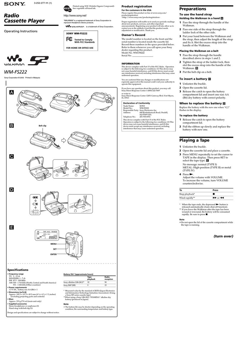
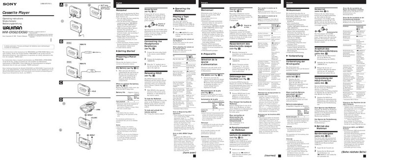
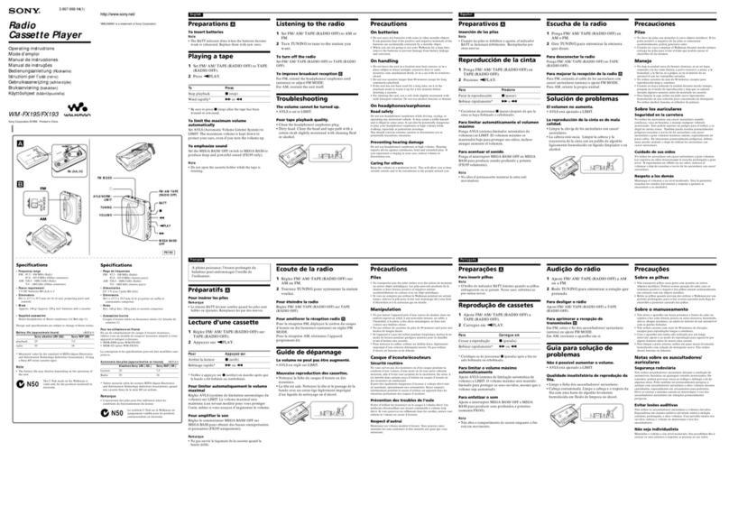
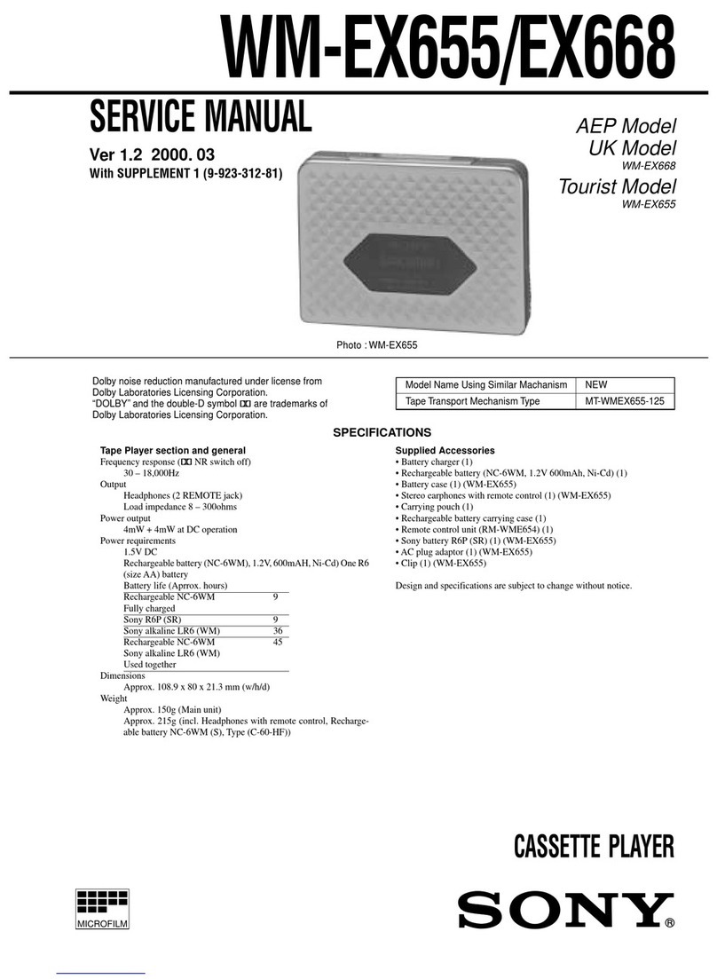
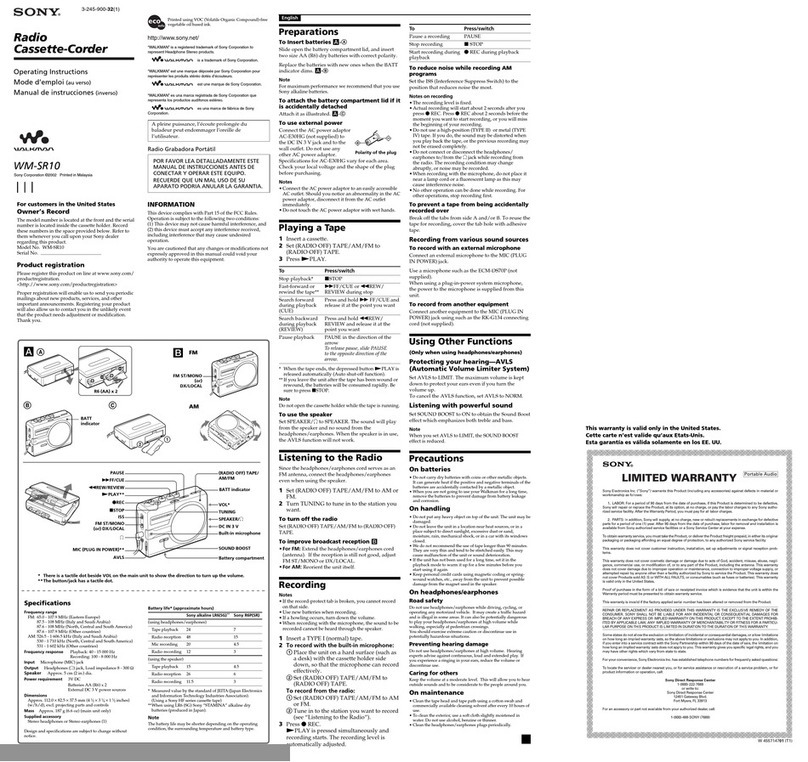
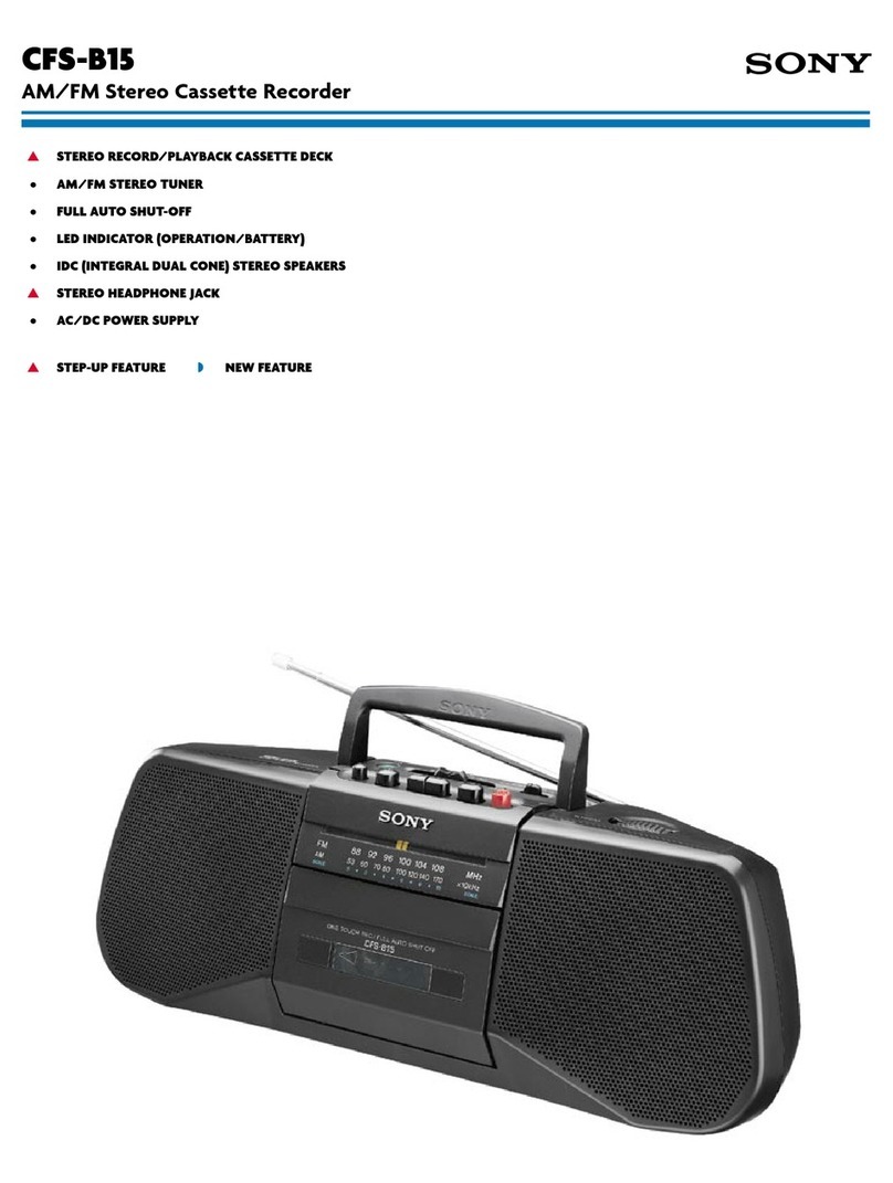
Sony WM-FX671 User manual

WM-FX671
US Model
AEP Model
SERVICE MANUAL
RADIO CASSETTE PLAYER
Manufactured under license from Dolby Laboratories
Licensing Corporation.
“DOLBY” and the double-D symbol aare trademarks
of Dolby Laboratories Licensing Corporation.
Model Name Using Similar Mechanism WM-EX678
Tape Transport Mechanism Type MT-WMEX672-162
SPECIFICATIONS
Sony Corporation
Personal Audio Company
Published by Sony Engineering Corporation
9-926-978-13
2002K1600-1
© 2002.11
Radio section
Frequency range FM : 87.5 – 108MHz
AM : 531 – 1.602 kHz
Tape section
Frequency response
(Dolby NR off) Playback: 40 – 15,000Hz
Output Headphones (2REMOTE) jack
Load impedance 8 – 300 Ω
General
Power requirements 1.5V
Rechargeable battery
One R6 (size AA) battery
Dimensions (w/h/d) Approx. 108.9 ×77.7 ×23.9 mm
(43/8×31/8×31/32inches), incl.
projecting parts and controls
Mass Approx. 145 g (5.2 oz)
Approx. 210 g (7.5oz) incl.
rechargeable battery and a cassette
Supplied accessories Battery case (1)
Stereo earphones (1)
Battery charge (1)
Rechargeable battery (NC-6WM, 1.2V, 600mAh,
Ni-Cb) (1)
Rechargeable battery carring case (1)
Carrying pouch (1)
Design and specifications are subject to change without notice
Ver 1.2 2002. 11

— 2 —
Notes on chip component replacement
• Never reuse a disconnected chip component.
• Notice that the minus side of a tantalum capacitor may be
damaged by heat.
Flexible Circuit Board Repairing
• Keep the temperature of soldering iron around 270˚C
during repairing.
• Do not touch the soldering iron on the same conductor of the
circuit board (within 3 times).
• Be careful not to apply force on the conductor when soldering
or unsoldering.
SAFETY-RELATED COMPONENT WARNING!!
COMPONENTS IDENTIFIED BY MARK !OR DOTTED LINEWITH
MARK !ON THE SCHEMATIC DIAGRAMS AND INTHE PARTS
LIST ARE CRITICAL TO SAFE OPERATION. REPLACE THESE
COMPONENTS WITH SONY PARTS WHOSE PART NUMBERS
APPEAR AS SHOWN IN THIS MANUAL OR IN SUPPLEMENTS
PUBLISHED BY SONY.
TABLE OF CONTENTS
1. SERVICE NOTE ······························································· 3
2. GENERAL ·········································································· 5
3. DISASSEMBLY
3-1. Case Block Assembly ····················································· 6
3-2. Belt (F2) ·········································································· 7
3-3. Cassette LidAssembly ···················································· 7
3-4. Reel OrnamentAssembly ··············································· 8
3-5. Main Board ····································································· 8
3-6. Motor (F2) (M901) ························································· 9
3-7. Holder Assembly····························································· 9
3-8. Pinch Lever (N)/(R) Assembly ····································· 10
3-9. Magnetic Head (HP901) ··············································· 10
4. MECHANICAL ADJUSTMENT ································ 11
5. ELECTRICAL ADJUSTMENT ·································· 11
6. DIAGRAMS
6-1. Block Diagram ······························································ 13
6-2. Printed Wiring Board ···················································· 16
6-3. Schematic Diagram (1/2) ·············································· 19
6-4. Schematic Diagram (2/2) ·············································· 22
6-5. IC Block Diagrams ······················································· 25
6-6. IC Pin Function Discription ·········································· 27
7. EXPLODEDVIEWS
7-1. Cabinet Block, Main Board ·········································· 29
7-2. Mechanism Deck Block················································ 30
8. ELECTRICAL PARTS LIST ······································· 31

— 3 —
p
(S3) ENTER
(S10) BAND
(S8)
MENU
(S6)
R43
(SIDE A)
Q15
(SIDE A)
PH1
(SIDE A)
SET
(S7)
(S1)
FWD
←
STOP
→
REV
Battery terminal
’
Battery terminal
‘
Square-wave
(sine wave)
10 Hz, -3.5 dB
AF OSC
Plunger (PM901)
Short
R TUME
SWITCH
(S901-2)
TAPE DETECT
SWITCH
(S901-1)
FF AMS
(S4)
REW AMS
(S5)
œ
REPEAT
(S9) M601
M
SECTION 1
SERVISE NOTE
[Service Mode]
The service mode enables to operate the mechanism ofWM-FX671
while the MAIN board is opened.
Rotation of the idler gear (A) (S side) is detected using the photo-
reflector (PH1) in the WM-FX671. PH1 is located on the MAIN
board, therefore the rotation of the idler gear (A) (S side) cannot be
detected by PH1 when the MAIN board is removed. As a result, the
motor cannot be controlled and cannot run correctly.
To repair the machine after the MAIN board is removed while the
main power is turned on, follow the procedures as described below.
1. Setting
1) Removethe cabinets referringto section“3. DISASSEMBLY”.
Open the MAIN board.
2) Connect the motor (M601) and the plunger solenoid (PM901)
tothe MAIN board usingthe jumperwires. When theextension
jig (1-769-143-11) (10 wires as a set) is used, they can be
connected easily.
3) Short the TAPE DETECT switch (S901-2), R TUME switch
(S901-1).
4) Connect an AF oscillator to resistor (R43).
5) Connect DC 1.3V from external regulated power supply to ‘
and ’terminals of the battery.
2. PRE-SET status
The PLAY, FF and REW modes can be entered only from the PRE-
SET status.
1) Check that the slider (NR) is in the center position (S1), and
the FWD/REV switch is also in the center position. When
these switches are not in the center position, set them to the
PRE-SET status as follows.
2) Move the FWD/REV switch (S1) to the same position as the
slider (NR) is set.
3) The slider (NR) can be moved when the main power of the
regulated power supply is turned OFF once then back ON.
Move the FWD/REV switch (S1) to the center position in
synchronism with the timing when the slider (NR) is moved.
3. FF, REW modes
1) Check that the PRE-SET status is set.
2) Connect square wave or sine wave to resistor (R43). (See
illustration below.)
3) Press the pswitch (S3) to enter the STOP mode.
4) Press the FF AMS switch (S4) and the REW AMS switch
(S5).
4. PLAY mode
1) Check that the PRE-SET status is set.
2) Connect square wave or sine wave to resistor (R43). (See
illustration below.)
3) Press the pswitch (S3) to enter the stop mode.
4) When the 9(REPEAT switch (S9) of the MAIN board is
pressed, the slider (N/R) moves once to the F side then moves
to the R side. When the FWD/REV switch (S1) is pressed in
the synchronism with the above timing, the machine can enter
the PLAY (R side) mode. Press the 9(REPEAT switch
(S9) again, and move the FWD/REV switch (S1) in the
synchronism with the motion of slider (NR). It enables the
machine to enter into the PLAY (F side) mode.
Note 1: When you fail to enter the PLAY mode, re-start from step
1) PRE-SET status.
Note 2: Regarding the 9(REPEAT (S9), p(S3),
FF AMS (S4), and REW AMS (S5) switches, use these
switches of the remote control unit as much as possible.
Note 3: If a headphones are used, the beep sound shows the timing
of the FWD/REV switch (S1).
– MAIN BOARD (SIDE B) —
— 4 —
[ Slider (NR) ] [Tape drive mechanism ]
Tape drive mechanism in PLAY mode
Tape drive mechanism in FF mode Tape drive mechanism in REW mode
Slider (NR)
Center
F side R side
Insert Flywheel (N)
Pulley (Reverse)
Clutch Assy
Motor Pulley
Gear (REEL)(S side)
Gear
(REEL)(T side)
Gear (NR)
(FWD : Left side
REV : Right side)
Idler Gear
Idler Gear (A)(S side)
Idler Gear
(A)(T side)
Insert Flywheel (R)
Cam Gear
Gear (Y)
Insert Flywheel (N)
Pulley (Reverse)
Clutch Assy
Motor Pulle
y
Gear
(REEL)(T side)
Idler Gear
(A)(T side)
Insert Flywheel (R)
Cam Gear
Gear (Y)
Gear (FR)
(FF : Left side)
Insert Flywheel (N)
Pulley (Reverse)
Clutch Assy
Motor Pulley
Gear
(REEL)(S side)
Idler Gear
(A)(S side)
Insert Flywheel (R)
Cam Gear
Gear (Y)
Gear (FR)
(REW : Right side)

— 5 —
SECTION 2
GENERAL
12345
6
7
8
9
!º!¡!™!£
!¢
•LOCATION OF CONTROLS
12REMOTE jack
2REW, AMS button
3“”, REPEAT button
4FF, AMS button
5OPEN knob
6Battery case
7Display window
8HOLD cknob
9SET button
!º MENU button
!¡ BAND, RADIO ON button
!™ ENTER, COUNTER RESET button
!£ p, RADIO OFF button
!¢ ∑VOL knob

— 6 —
SECTION 3
DISASSEMBLY
Note : Disassemble the unit in the order as shown below.
Note : Follow the disassembly procedure in the numerical order given.
Set Case block
assembly
Belt (F2)
Cassette lid assembly Main board
Reel ornament
assembly
Motor (F2)
(M901) Holder
assembly Pinch lever (N)/(R)
assembly Magnetic hea
d
(HP901)
3-1. CASE BLOCK ASSEMBLY
3
Screw (M1.4
×
2.5)
2
Two screws
(M1.4
×
2.5)
1
Battery case Lid
5
Remove the case block assembly
in the direction of the arrow.
4
Two screws
(M1.4
×
2.5)
knob (HOLD)
Claw
S2
Note:
When assembling the case
block assembly, align the
knob (HOLD) with the
position of S2.

— 7 —
3-2. BELT (F2)
3
Belt (F2)
2
Terminal boar
d
(Battery
’
)
1
Remove solder from
the battery terminal board.
Belt (F2)
Belt threading
3-3. CASSETTE LID ASSEMBLY
5
Cassette lid assembly
4
Shaft
3
Open the cassette lid
1
Screw (M1.4
×
2.0)
2
Two screws (M1.4
×
2.0)

— 8 —
3-4. REEL ORNAMENT ASSEMBLY
1
Reel Ornament assembly
Remove the assembly while removin
g
the three claws and boss carefully.
Note:
Claw
Claw
3-5. MAIN BOARD
SLIDER
9
Remove soldeing
(two points)
from plunger solenoid.
7
Screw (B1.7
×
3)
tapping
6
Screw (B1.7
×
3)
tapping
3
Screw (M1.4)
8
Screw (M1.4)
2
Head flexible board
4
Screw (M1.4)
Bracket assy
0
Remove soldeing
(four points) from
motor.
When assembling the MAIN board,
align the slider with the position of S1.
Note:
5
Screw (M1.4
)
1
Remove soldering
from Head flexible
board.

— 9 —
3-6. MOTOR (F2) (M901)
1
Two screws (M1.4)
2
Motor (F2) (M901)
Toothed lock
3-7. HOLDER ASSEMBLY
4
Screw (M1.4)
2
Shaft
6
Shaft
1
Two screws (M1.4
×
1.4)
3
Lock lever (B)
0
Remove the holder
assembly in the directio
n
of the arrow.
8
Remove soldering
from Head flexible board.
5
Lock lever (S)
9
Head flexible
board
7
Cassette bracket assembly

— 10 —
3-8. PINCH LEVER (N) / (R) ASSEMBLY
Claw
Claw
2
Remove the pinch lever
(N) assembly in the direction
of the arrow.
Note:
Be careful of the claw
1
Remove the pinch lever
(R) assembly in the direction
of the arrow.
Note:
Be careful of the claw
3-9. MAGNETIC HEAD (HP901)
1
Remove the magnetic head (HP901)
in the direction of the arrow.

— 11 —
SECTION 4
MECHANICAL ADJUSTMENT SECTION 5
ELECTRICAL ADJUSTMENT
PRECAUTION
1. Specified voltage: 1.3 V (DC)
2. Switch and control position
MENU switch
aNR : OFF
AVLS : OFF
SOUND : OFF
HOLD : OFF
VOL : MAX
TestTape
Tape Speed Adjustment
Procedure:
1. Enter the FWD playback mode.
2. Adjust RV601 sothat thevalueofthe frequencycounterreading
becomes 3,000 Hz.
Specification value:
Frequency counter
2,955 Hz – 3,060 Hz
3. Check that the frequency deviation at the beginning and ending
of a tape is within 1.5 % (45 Hz).
PRECAUTION
1. Clean the following parts with a denatured-alcohol-moistened
swab:playback head pinch roller
rubber belts capstan
2. Demagnetize the playback head with a head demagnetizer.
3. Do not use a magnetized screwdriver for the adjustments.
4. After the adjustments, apply suitable locking compound to the
parts adjusted.
5. The adjustments should be performed with the rated power
supply voltage unless otherwise noted.
•Torque Measurement
Mode
FWD
FWD
Back Tension
REV
REV
Back Tension
FF, REW
Torque Meter
CQ-102C
CQ-102C
CQ-102RC
CQ-102RC
CQ-201B
Meter Reading
15 to 25 g•cm
(0.21 to 0.34 oz•inch)
Less than 2.0g•cm
(Less than 0.028 oz•inch)
15 to 25 g•cm
(0.21 to 0.34 oz•inch)
Less than 2.0g•cm
(Less than 0.028 oz•inch)
More than 50 g•cm
(More than 0.69 oz•inch)
Signal
3 kHz, 0 dB Used for
Tape Speed Adjustment
Tape
WS-48A
Test tape
WS-48A
(3kHz, 0dB)
Set
2
REMOTE jack (J701)
16
Ω
Frequency counter
+
–
[MAIN BOARD] — SIDE B —
‘?
‘?
’?
RV601
L2
T2
TP6
TP5 IC2
13
241
12
T1 RV1
RV601 :Tape speed
adjustment
RV1 : FM VCO adjustment
T2 : AM IF adjustment
L2 : FM frequency coverage
adjustment
T1 : AM frequency coverage
adjustment
TP1
Adjustment Parts Location :
[MAIN BOARD] — SIDE A —
TAPE SECTION

— 12 —
[AM]
BAND switch : AM
[FM]
BAND : FM
• Repeat the procedures in each adjustment several times.
AM FREQUENCY COVERAGE ADJUSTMENT
Adjust for a maximum reading on level meter.
T1 531 kHz
FM FREQUENCY COVERAGE ADJUSTMENT
Adjust for a maximum reading on level meter.
L2 76 MHz
FMVCO Adjustment
Procedure :
1. Connect frequency counter to the positions shown below.
2. Tune the set to 98 MHz.
3. Adjust RV1 so that the value of the frequency counter reading
becomes 19 kHz.
Specification Value :
Frequency counter
18,900 – 19,100 Hz
TUNER SECTION
0.01
µ
F
FM RF signal
generator
to ANT (TP1)
22.5kHz frequency deviation by 400Hz signal.
Output level : as low as possible
Put the lead-wire
antenna close to
the set.
30% amplitude modulation by 400Hz
signal.
Output level : as low as possible
AM RF signal
generator
16
Ω
set +
–
level mete
r
2
REMOTE jack (J701)
AM IF ADJUSTMENT
Adjust for a maximum reading on level meter.
T2 450 kHz
0.01
µ
F
FM RF signal
generator
to ANT (TP1
)
Carrier frequency : 98MHz
IModulation : no modulation
Output level : 0.1V (100dB)
Frequency counte
r
1
µ
F+
–
100k
Ω
TP5
(IC2 Pin
!™
)
TP6
(IC2 Pin
9
)
0dB=1µV
Adjustment Location: MAIN board (See page 11)

WM-FX671
SECTION 6
DIAGRAMS
— 13 — — 14 — — 15 —
6-1. BLOCK DIAGRAM

○○○○○○○○○○○○○○○○○○○○○○○○○○○○○○○○○○○○○○○○○○○○○○○○○○○○○○○○○○○○○○○○○○○○○○○○○○○○○○○○○○○○○○○○○○○○○○○○○○○○○○○○○○
○○○○○○○○○○○○○○○○○○○○○○○○○○○○○○○○○○○○○○○○○○○○○○○○○○○○○○○○○○○○○○○○○○○○○○○○○○○○○○○○○○○○○○○○○○○○○○○○○○○○○○○○○○
WM-FX671
— 17 — — 18 —
6-2. PRINTEDWIRING BOARD
Note on Printed Wiring Board:
•X: parts extracted from the component side.
•Y: parts extracted from the conductor side.
•Through hole is omit.
•b: Pattern from the side which enables seeing.
Caution:
Pattern face side: Parts onthe patternfaceside seen from
(SIDE B) the pattern face are indicated.
Parts face side: Parts on the parts face side seen from
(SIDE A) the parts face are indicated.
— 16 —
12
A
B
C
D
E
F
G
H
3456789101112131415161718192021
• Semiconductor Location
Ref. No. Location Ref. No. Location
D1 A-14
D2 B-14
D3 F-14
D4 C-15
D5 B-8
D6 C-13
D101 C-9
D201 C-9
D301 C-9
D302 B-9
D303 B-9
Ref. No. Location
D304 B-8
D305 G-9
D801 D-4
D802 E-3
D803 D-3
D804 D-3
IC1 B-14
IC2 D-14
IC3 D-17
IC4 F-18
IC5 D-18
IC6 C-19
IC301 F-17
IC302 E-9
IC601 D-19
IC801 D-3
Q1 D-16
Q2 C-16
Q3 B-13
Q4 B-14
Q5 D-15
Q6 C-15
Q7 B-13
Q8 C-16
Q9 D-6
Q10 C-13
Q11 D-15
Q12 E-16
Q13 E-13
Q14 B-13
Q15 C-4
Ref. No. Location
Q16 C-15
Q17 C-15
Q18 F-15
Q19 F-16
Q20 C-6
Q301 E-19
Q302 F-16
Q303 F-16
Q304 F-9
Q305 F-9
Q601 C-19
Ref. No. Location Ref. No. Location
Q602 C-19
Q801 D-3
Q802 C-2
Q803 D-2
Q804 C-3
Q805 C-2

WM-FX671
— 19 — — 20 —
6-3. SCHEMATIC DIAGRAM (1/2)
Note
• All capacitors are in µF unless otherwise noted. pF: µµF
50 WV or less are not indicated except for electrolytics
and tantalums.
• All resistors are in Ωand 1/4W or less unless otherwise
specified.
• % : indicates tolerance.
•U: B+ Line.
•C: panel designation.
•H: adjustment for repair.
• Powervoltage isdc1.5V and fedwithregulated dc power
supply from battery terminal.
• Voltages and waveforms are dc with respect to ground
under no-signal (detuned) conditions.
no mark : FM/AM, STOP (TAPE)
( ) : FM
[ ] : AM
< > : PLAY (TAPE)
• Voltagesare taken withaVOM(Inputimpedance10 MΩ).
Voltage variations may be noted due to normal produc-
tion tolerances.
• Waveforms are taken with a oscilloscope.
Voltage variations may be noted due to normal produc-
tion tolerances.
• Circled numbers refer to waveforms.
• Signal path.
F: FM
E: PLAY (TAPE)
•Waveform
51.7kHz
1
TP32 10µsec/div
5V/div
12
A
B
C
D
E
F
G
H
I
3456789101112131415161718192021
— 21 —

WM-FX671
— 22 — — 23 —
6-4. SCHEMATIC DIAGRAM (2/2)
— 24 —
Note
• All capacitors are in µF unless otherwise noted. pF: µµF
50 WV or less are not indicated except for electrolytics
and tantalums.
• All resistors are in Ωand 1/4W or less unless otherwise
specified.
• % : indicates tolerance.
•U: B+ Line.
•C: panel designation.
•H: adjustment for repair.
• Powervoltage isdc1.5V and fedwithregulateddc power
supply from battery terminal.
• Voltages and waveforms are dc with respect to ground
under no-signal (detuned) conditions.
no mark : PLAY
• Voltagesare takenwithaVOM(Inputimpedance10 MΩ).
Voltage variations may be noted due to normal produc-
tion tolerances.
• Waveforms are taken with a oscilloscope.
Voltage variations may be noted due to normal produc-
tion tolerances.
• Circled numbers refer to waveforms.
• Signal path.
F: FM
E: PLAY (TAPE)
2IC2 !¶ VCO 5µsec/div
50mV/div 3IC801 5PLAY 5µsec/div
1V/div
75kHz
4IC3 &¢ XOUT 5µsec/div
0.5V/div
•Waveform
12
A
B
C
D
E
F
G
H
I
J
K
L
M
345678910111213141516171819

— 25 —
6-5. IC BLOCK DIAGRAMS
V1
PW 2
W3
GND 4
OSC 5
DR 6
VREF 7
START 8
VSP 9
IN+ 10
PV
20 U
19
PU
18 GND
17 VCC
16 FC
15
TC1
14 TC2
13
R1
12 OUT
11
MOTIVE
CONTROL
CIRCUIT
MOTIVE/
OSC MOTIVE
LOGIC SOFT SWITCH
PRE DRIVER
INVERTER
BIAS
REFERENCE
VOLTAGE
SPEED
CONTROL CURRENT
CONTROL
OUTPUT
BIAS
+
–
IC302 NJM2185AV-TE2
37
38
39
40
41
42
43
44
45
46
47
48
24
23
22
21
20
19
18
17
16
15
14
13
123456789101112
3536 34 33 32 31 30 29 28 27 26 25
N.C.
REF
V REF
GND
REV REC L
REV REC R
FWD REC R
FWD REC L
VCC2
MONITOR L
MONITOR R
N.C.
GND
MIC IN L
NF L
RADIO IN L
MIC IN R
NF R
RADIO IN R
MIC OUT R
MIC OUT L
REC IN L
REC IN R
N.C.
N.C.
REC MUTE
MIC/RADIO
FWD/REV
REC/PLAY
CONT F
CONT A
(FWD)
PLAY(REV)
(REV)
PLAY(FWD)
PLAY(FWD)
(REV)
(REV)
PLAY(FWD)
PLAY
REC
CONT B
CONT C
CONT D
CONT E
N.C.
N.C.
MIC REG REF
MIC REG
REC BIAS REG REF
REC BIAS REG
OSC
BASE
VCC1
VCCRF
ALC
GND
N.C.
SYSTEM CONTROL
V REF
REV
REC
AMP
FWD
REC
AMP
MONITOR
AMP
DET
MIC
REGULATOR REC BIAS REGULATOR
ALC
AMP
L
ALC
AMP
R
VCC2
( ):REC
GND
AFC DIODE(A)
RF IN
OFC DIODE(C) MIX OUT
VCC
OSC
RF OUT
1 2 3 4
5678
RF
REG
MIX
OSC
IC2 TA2022AFN-ELIC1 TA7371AF-EL

— 26 —
891014 13 12
21 3
A-CH BLOCK
11
7654
G2 G1 V/I
WEIGHT
BIAS
CIRCUIT
+
–
+
–
GM
SUM
V+
SW
VEXT
OUTA
DCA
DETA
INA
GND
IREF
VREF
OUTB
DCB
DETB
INB
B-CH BLOCK: SAME AS A-CH.
PRE A PRE B MIX
PW B
PW A
PW C
BST
MT TC
BASE
RF IN
PW GND
OUT B
OUT C
OUT A
VCC
RF OUT
VREF OUT
BST NF
BST OUT
PW IN C
LPF
EQ A
PW NF A
PW IN A
PW IN B
PW NF B
3
IN A-R
5
PRE NF-A
6
PRE OUT A
7
MTL DRV A
8
MTL DRV B
9
PRE OUT B
10
PRE NF-B
11
AMS IN
12
IN B-R
4
IN B-F
2
IN A-F
1
21
20
19
18
17 GND
16 AMS DET
15
AMS MIX
14
AMS SW
13
22
23
24
38
C-AMP SW 37
PW SW 42
MT SW 41
F/R SW 44
BST SW 43
M/N SW 46
PRE GND 47
VREF IN 48
PRE SW 45
AMS OUT 40
BEEP 39
262728293031323334
DET
36
AGC IN
35
+
–
+
–
+
–
+
–
+
–
+
–
EQ B
25
RIPPLE
FILTER
AGC
DET
BEEP
VREF
SWITCH COMPARATOR
MTL DRV
IC301 TA2123AF (EL)
IC601 MM1279XVBE

— 27 —
6-6. IC PIN FUNCTION DESCRIPTION
•IC3 TC9327AF-604
Pin No.
1 to 4
5 to 22
23
24
25
26
27
28
29
30
31
32
33
34
35
36
37
38
39
40
41
42
43
44
45
46
47
48
49
50
I/O
O
O
O
O
—
—
O
O
O
O
O
I
I
I
I
I
I
O
I
O
I
I
I
I
I
O
I/O
O
O
O
Description
Common terminal.
Segment output terminal.
Dolby control terminal. (L: ON, Hi-imp: OFF)
Motor speed control terminal.
Not used
Not used
PRE AMP control terminal.
MUTE control terminal (L: MUTE ON).
HEAD select terminal (PLAY mode) (L: FWD, H: REW).
BAND control output (L: FM, H: AM).
Remote control data output.
TAPE error erase detect terminal. (FWD).
TAPE error erase detect terminal. (REV).
Remote control data input.
Input when the key is pressed during HOLD (H=AD Vref).
Tape end Locking detect input terminal.
Tape sound existing or not-exiting detect (L: Music exists: H: Music does not exist).
Terminal for controlling the rotation detect circuit.
Rotation detect input.
DDC control terminal (H: DDC ON).
HOLD detect input (L: HOLD ON).
Voltage detect input.
KEY input terminal.
TAPE rotating direction detect terminal.
AD IN 1, 2, 3 reference viltage interrupt terminal.
E2PROM CS control terminal.
E2PROM DATA I/O.
E2PROM CLOCK terminal.
BEEP (when TC: 1.6kHz, when CF: 3.0kHz).
MOTOR control terminal.
Pin Name
COM 1 to
COM 4
S1 to S18
DOLBY VCC
CTL
S1/2 CTL
RADIO/MIC
F/R CTR (REC)
PRE CTL
MUTE CTL
F/R CTL PLAY
BAND AM/FM
R DATA OUT
F TUME
R TUME
R DATA IN
HOLD SENS
OSC CTL
AMS IN
PHOTO CTL
PHOTO IN
DDC1 CTL
HOLD SW
BATT DET
KEY IN
F/R SW
(VCC) AD REF
CS
M DATA I/O
M CLOCK
BEEP
MOTOR CTL

— 28 —
Pin No.
51
52
53
54
55
56
57
58
59
60
61
62
63
64
65
66
67
68
69
70
71
72
73
74
75
76
77
78
79
80
I/O
O
I
—
O
O
O
O
O
O
O
O
O
I
I
O
O
I
O
—
I
I
—
I
O
I
—
—
—
—
—
Description
MOTOR control terminal.
TAPE detect terminal. (L: ON, H: OFF)
Not used
Terminal for controllingAVLS (when ON=H).
Tone control terminal (L: normal, Hi-imp: MEGA BASS).
Revive control terminal.
Tone control terminal (L: GRV, H: MB).
AMP control output (H: AMP ON).
Terminal for controlling DOLBY circuit (L: OFF, Hi-imp: ON).
PL control terminal.
DDC control terminal (L: OFF, Hi-imp: ON).
RADIO system control terminal (L: RADIO ON).
TEST terminal (Normal operation at L or NC).
IF input.
TUNER sensitivity select terminal (H: LOCAL, L: DX).
Phase comparator output.
External interrupt terminal (Interrupt by key input).
FM MONO/STEREO select terminal (H: MONO, L: ST).
Power supply Ground terminal.
FM local oscillator input.
AM local oscillator input.
Power supply voltage.
RESET terminal (H during operation).
Terminal to which external oscillator is connected.
Terminal to which external capacitor is connected to stabilize crystal oscillator power supply.
Terminal to step-up power supply voltage for LCD drive. (3V)
Terminal to step-up power supply voltage for LCD drive.
Terminal for 1.5V constant voltage power supply of LCD drive.
Pin Name
MOTOR DIR
TAPE
REC CTL
AVLS CTL
BST CTL
RV CTL
MB/GRV CTL
AMP CTL
DOLBY CTL
PM CTL
DDC2 CTL
RADIO CTL
TEST
IF IN
LOCAL/DX
DO
WAKE UP
MONO/ST
GND
FM IN
AM IN
VDD
RESET
XOUT
XIN
VXT
VLCD
C1
C2
VEE
Table of contents
Other Sony Cassette Player manuals

Sony
Sony TCM-200DV - Cassette Recorder User manual

Sony
Sony J-1 User manual

Sony
Sony WM-EX655 User manual

Sony
Sony TC-WA8ESA User manual

Sony
Sony Sports Walkman WM-FS111 User manual

Sony
Sony Sports Walkman WM-FS497 User manual

Sony
Sony CFS-515S User manual

Sony
Sony TC-W21 User manual

Sony
Sony TCS TCS-30D User manual

Sony
Sony Walkman WM-FX490 User manual

Sony
Sony TC-WR350Z User manual

Sony
Sony TCS-580V User manual

Sony
Sony TC-WR465 User manual

Sony
Sony WM-DDIII User manual

Sony
Sony CF-SW1000T User manual

Sony
Sony TCW-E475 User manual

Sony
Sony TC-K333ESG User manual

Sony
Sony Walkman WM-FX661 User manual

Sony
Sony TC-K611S User manual

Sony
Sony Walkman wm-FX105 User manual