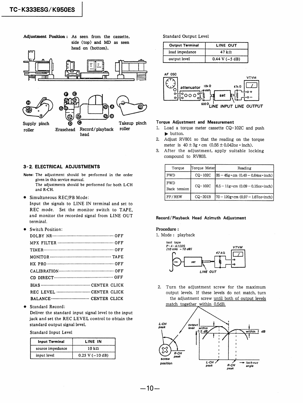
Sony TC-K333ESG User manual

TC-K333ESG
Dolby
noise
reduction
manufactured
under
license
from
Doiby
Laboratories
Licensing
Corporation.
“DOLBY”
and
the
double-D
symbot
0G
are
trademarks
of
Dolby
Laboratories
Licensing
Corporation.
SPECIFICATIONS
Recording
system
4-track
2-channe!
stereo
General
Bias
AC
bias
Power
requirements
Heads
Erase
head
x
1
(S&F
head)
Recording
head
x
1
(LA
head)
Playback
head
x
1
(LA
head)
Motors
Capstan
motor
x
1
(direct
drive
linear
torque
BSL
motor)
Reel
motor
x 1
(DC
motor)
Wow
and
flutter
0.024%
WRMS
(NAB)
Fast-forward
and
rewind
time
Approx.
90
sec.
(with
C-60
cassette)
Frequency
response
(DOLBY
NR
OFF)
TYPE
IV
cassette
15-—
22,000
Hz
(+3
dB,
DIN)
(Sony
METAL-ES)
15-—16,000
Hz
(OVU
recording)
:
TYPE
il
cassette
15—20,000
Hz
(+3
dB,
DIN)
Sony
UX-S)
TYPE
|
cassette
15-18,000
Hz
(+3
dB,
DIN)
(Sony
HF-S)
.
Signal-to-noise
ratio
(at
peak
level
)
Dolby
NR
switch
OFF
B-TYPE
|
C-TYPE
ON
ON
TYPE
IV
(Sony
METAL-ES)
70
dB
|
76
dB
TYPE
lI
(Sony
UX-S)
59
dB
|
68dB
|
74
4B
TYPE
|
(Sony
HF-S)
57dB
|
66dB
|
72
dB
Total
harmonic
distortion
Inputs
0.8%
(with
Sony
METAL-ES
cassette)
Line
inputs
Sensitivity
77.5
mV
(-—20
dB)
(phono
jacks)
Input
impedance
|
50k
ohms
CD
DIRECT
INPUT
|
Input
impedance
50k
ohms
Outputs
Line
outputs
Rated
output
level
|
0.44
V
(—5
dB)
ata
(phono
jacks)
load
impedance
47k
ohms
Load
impedance
Over
10k
ohms
Headphones
Output
level
0-3
mW
at
a
load
(stereo
phone
jack)
impedance
of
32
ohms
Power
consumption
Dimensions
Weight
Model
Name
Using
Similar
Mechanism
|
New
|
Tape
Transport
Mechanism
Type
TCM-
200D
1
US
Model
Canadian
Model
AEP
Model
UK
Model
TC-K950ES
E
Model
TC-K333ESG
AEP
model:
220
V
AC,
50/60
Hz
UK
model
:
240
V
AC,
50
Hz
US,
Canadian
models
:
120
V
AC,
60
Hz
E
model
:
120,
220,
or
240
V
AC
adjustable,
50/60
Hz
31
W
Except
UK
model
:
Approx.
470
x
140
x
380
mm
(w/h/d)
(185,
x
5,
x
15
inches)
UK
model
:
Approx.
430
x
140
x
380
(17x
5,
15
inches)
including
projecting
parts
and
controls
Approx.
11.7
kg
(25
ibs
13
02)
Model
for
the
United
Kingdom:
Approx.
11
kg
(24
Ibs
5
02)
Supplied
accessories
Audio
connecting
cord
(2)
Wireless
remote
control
unit
RM-J702
(1)
Sony
R6
(size-AA)
batteries
(2)
Screws
(8)
(Except
UK
model)
A
remote
commander
and
Sony
R6
batteries
are
supplied
with
UK,
E
models.
Design
and
specifications
subject
to
change
without
notice.
Note
This
appliance
conforms
with
EEC
Directive
87/308/EEC
regarding
interference
suppression.
STEREO
CASSETTE
DECK
SONY.

TC-K333ESG/K950ES
TABLE
OF
CONTENTS
section
Title
Page
SPECIFICATIONS
i
a
ee
ee
1
MODEL
IDENTIFICATION
re
ee
ee
3
SAFETY
CHECK-OUT
cress
ecssecccccercccescceceees
3
1.
GENERAL
+++ee
errr
rere
cette
eee
e
eter
eeeeeeeeeennees
4
2.
DISASSEMBLY
rrr
re
ee
ee
5
3.
ADJUSTMENTS
3-1.
Mechanical
Adjustments
-++sssssrrreee
reer
7
3-2.
Electrical
Adjustments
:+++++s+rerteeeer
eres
10
4.
DIAGRAMS
4-1-1.
IC
Block
Diagrams+-++++seereseeeeeeeeees
15
4-2-1.
IC503,
505
(CX20188)
Pin
Functions::::-
15
4-2-2.
IC801
(M50964-220SP)
Pin
Functions
---
16
4-1-2.
Ic
Block
Diagrams
Corer
reer
verre
sceseees
17
4-3,
Block
Diagram
cecsrsrrtseee
eect
e
er
eeeeeeees
17
4-4,
Semiconductor
Lead
Layouts
-+++++++-+++*>
21
4-5.
Circuit
Boards
Location
-sr++ssssrrereeeees
21
4-6.
Printed
Wiring
Boards
—
Audio
Section
—
cceerer
reece
eee
eeeeeeees
22
4-7,
Schematic
Diagram
|
—
Audio
Section
—
cerrrserercecetereeeeeees
27
4-8.
Printed
Wiring
Boards
—Syscon
Section
—
srrrrerscrereceseeeeeees
32
4-9.
Schematic
Diagram
—
Syscon
section
rr
ee
37
5.
EXPLODED
VIEWS
5-1.
Panel
Section
-crrssercreee
eset
sere
enc
cree
42
5-2.
Chassis Section
«cssccesece
reece
eeeeeeceeees
44
5-8.
Mechanism
Section
(1)
(TCM~200D1)
srrerecercee
eer
eeceeeeeeeenees
A5
5-4.
Mechanism
Section
(2)
(TCM-200D1)
srrrereereceecereeeeecseneeens
46
6.
ELECTRICAL
PARTS
LIST
--++csscrreeeeeeeeeeeee
AT
SAFETY-RELATED
COMPONENT
WARNING!!
COMPONENTS
IDENTIFIED
BY
MARK
A
OR
DOTTED
LINE
WITH
MARK
A
ON
THE
SCHEMATIC
DIAGRAMS
AND
IN
THE
PARTS
LIST
ARE
CRITICAL
TO
SAFE
OPERATION.
REPLACE
THESE
COMPONENTS
WITH
SONY
PARTS
WHOSE
PART
NUMBERS
APPEAR
AS
SHOWN
IN
THIS
MANUAL
OR
IN
SUPPLEMENTS
PUB-
LISHED
BY
SONY.
Flexible
Circuit
Board
Repairing
*
Keep
the
temperature
of
the
soldering
iron
around
270
during
repairing,
*
Do
not
touch
the
soldering
iron
on
the
same
conductor
of
the
circuit
board
(within
3
times).
*
Be
careful
not
to
apply
force
on
the
conductor
when
soldering
or
unsoldering.
Notes
on
chip
component
replacement
«
Never
reuse
a
disconnected
chip
component.
«
Notice
that
the
minus
side
of
a
tantalum
capacitor
may
be
damaged
by
heat,
Dolby
noise
reduction
and
HX
Pro
headroom
extension
manufactured
under
license
from
Dolby
Laboratories
Licensing
Corporation.
HX
Pro
originated
by
Bang
&
Olufsen.
Operating
voltage
.
Before
connecting
the
unit
to
the
power
source,
check
that
the
operational
voltage
of
your
unit
is
the
same
as
the
local
power
supply.
Where
purchased
|
Operating
voltage
AEP,
WG
model
|
220
V
AC,
50/60
Hz
UK
model
240
V
AC,
50
Hz
US,
120
V
AC,
60
Hz
Canadian
model
E
model
120,
220
or
240
V
AC
adjustable,
50/60
Hz
A
voltage
selector
is
located
on
the
rear
panel.
If
the
selector
must
be
reset,
disconnect
the
AC
power
cord
and
set
the
selector
to
the
appropriate
voltage.
VOLTAGE
selector
VOLTAGE
ATTENTION
AU
COMPOSANT
AYANT
RAPPORT
A
LA
SECURITE!
LES
COMPOSANTS
IDENTIFIES
PAR
UNE
MARQUE
/\
SUR
LES
DIAGRAMMES
SCHEMATIQUES
ET
LA
LISTE
DES
PIECES
SONT
CRITIQUES
POUR
LA
SECURITE
DE
FONCTIONNEMENT.
NE
REMPLACER
CES
COM-
POSANTS
QUE
PAR
DES
PIECES
SONY
DONT
LES
NUMEROS
SONT
DONNES
DANS
CE
MANUEL
OU
DANS
LES
SUPPLEMENTS
PUBLIES
PAR
SONY.
—_2—

|
TC-K333ESG/K950ES
MODEL
IDENTIFICATION
SAFETY
CHECK-OUT
—
Specification
Label
—
After
correcting
the
original
service
problem,
perform
the
following
safety
check
before
releasing
TC-
K333ESG
the
set
to
the
customer:
TC-
K950ES
Check
the
antenna
terminals,
metal
trim,
‘‘metallized”
knobs,
screws,
and
all
other
exposed
metal
parts
for
AC
leakage.
Check
leakage
as
described
below.
SONY:
=
wo.
1.G,@
STEREO
CASSETTE
DECK
EEA
eee
WML
LLL
The
AC
leakage
from
any
exposed
metal
part
to
earth
ground
and
from
all
exposed
metal
parts
to
any
exposed
metal
part
having
a
return
to
chassis,
must
*
not
exceed
0.5mA
(500
microampers).
Leakage
current
can
be
measured
by
any
one
of
three
SERIAL
NO.
methods:
|
MADE
IN
JAPAN
1.
A
commercial
leakage
tester,
such
as
the
Simpson
229
or
RCA
WT-S40A.
Follow
the
manufacturers’
instructions
to
use
these
instru-
US,
Canadian
Models:
AC:
120V
60Hz
31W
ments.
AEP,
West
Germany
Model:
AC:
220V
\50/60Hz
31W
nw
A
battery-operated
AC
milliammeter.
The
Data
Precision
245
digital
multimeter
is
suitable
for
UK
Model:
AC:
240V
“U50/60Hz
31W
this
job.
E
Model:
AC:
120,
220,
240V
;
:
T\)50/60Hz
31W
.
3.
Measuring
the
voltage
drop
across
a
resistor
by
means
of
a
VOM
or
battery-operated
AC
volt-
meter.
The
“limit”
indication
is
0.75
V,
so
analog
meters
must
have
an
accurate
low-
voltage
scale.
The
Simpson
250
and
Sanwa
SH-63Trd
are
examples
of
a
passive
VOM
that
is
suitable.
Nearly
all
battery
operated
digital
multimeters
that
have
a
2V
AC
range
are
suitable.
(See
Fig.
A)
To
Exposed
Metal
Parts
on
Set
AC
voltmeter
|
|
«(0.78
V)
=
Earth
Ground
Using
an
AC
voltmeter
to
check
AC
leakage.

TC-K333ESG/K950ES
SECTION
1
GENERAL
LOCATION
AND
FUNCTION
OF
CONTROLS
fteseiece
POWER
switch
|
2|Remote
sensor
You
can
remotely
control
this
cassette
deck
with:
—
A
remote
commander
that
has
an
mark
and
comes
with
a
Sony
amplifier
or
receiver
and
which
can
be
used
to
control
a
cassette
deck.
—
An
optional
Sony
remote
commander
that
has
an
mark.
/3|LINEAR
COUNTER
|4|RESET
button
MEMORY
button
DISPLAY
MODE
button
|5
|
Dolby
HX
PRO
button
6
|
DOLBY
NR
(noise
reduction)/
MPX
FILTER
switch
MONITOR
switch
[8
|INPUT
switch
[9
|PEAK
PROGRAM
METER
REC
(recording)
LEVEL
PHONE
(headphones)LEVEL
control
Remote
Commander
(>
[>] [>]
[IN]
&
(open/close)
button
for
opening
and
closing
the
cassette
holder
[2]
DISPLAY
button
for
selecting
the
display
mode
Counter
buttons
RESET
button
for
resetting
the
counter
to
zero
MEMORY
button
for
activating
and
deactivating
the
Memory
function
Ceara
jack
(stereo
headphone
jack)
REC
EQ
CAL
(recording
equalization
calibration)
switch
(LOW,
NORMAL,
HIGH)
19]
Tape
operation
buttons
and
indicators
<4
(rewind)
button
(gi
(stop)
button
>
(play)
button
and
indicator
bP
(fast-forward)
button
@
REC
(record)
button
and
indicator
il
PAUSE
button
and
indicator
O
REC
MUTE
(record
muting)
button
20]
AMS(Automatic
Music
Sensor)
buttons
TIMER
switch
[4]
Tape
operation
buttons
<q
/p
|
(AMS*)
buttons
for
locating
selections
sequentially
<<
(leftward
fast
winding)
button
pp
(rightward
fast
winding)
button
»
(forward
play)
button
@
(record)
button
@
(stop)
button
II
(pause)
button
©
(record
muting)
button
[s]cp
(Compact
Disc)
buttons
(for
Sony
CD
players)
If
(pause)
button
Ke<q/bP1
(AMS)
buttons
for
locating
selections
sequentially
[6]CD
SYNCHRO
buttons
for
synchronized
recording
with
a
Sony
CD
player
(see
procedure
below)
STOP
(synchronized
recording
stop)
button
START
(synchronized
recording
start)
button
STANDBY
(synchronized
recording
standby)
button
*
AMS
is
an
abbreviation
for
Automatic
Music
Sensor.
Procedure
for
Synchronized
Recording
with
a
CD
Player

SECTION
2
DISASSEMBLY
NOTE:
Follow
the
disassembly
procedure
in
the
numerical
order
given.
:
JOINT
LEVER
2
CASSETTE
HOLDER
©
SPRING
4)
x
@
CASSETTE
HOLDER
ORNAMENTAL
PLATE
@ORNAMENTAL
PLATE
SCREWS,
*
<(h
PINCH
LEVER//LEVER
FR/HEAD
+B
26x6
(2
pes)
@-—
O:
PINCH
LEVER
S
[1].
[2]
:
PINCH
LEVER
T
A\
A\:
LEVER
FR
ZA\
STOPPER
WASHER
1.5
A\
LEVER
FR
[2]
PINCH
LEVER
T
N
O-—
1
stopper
WASHER
2.3
@
LEVER
PS
@
PINCH
LEVER
S

COMPARATOR
BOARD//CAPSTAN
BOARD//FLYWHEELS//FG
BOARD
&
SCREWS,
+PS
3x6
(2
pes.)
A\.Z\
:
COMPARATOR
BAORD
é.
@—
@
:
CAPSTAN
BOARD
WASHER
(1]—[3]
:
FG
BOARD
(after
removal
of
1
and
2)
Note:
To
remove
the
whole
unit
assembled
on
CAPSTAN
DECK.
(D1)
ASSY,
remove
4
screws
marked
x.
FLYWHEEL
(S)
@
SCREWS,+
BVTT
3x5
(2
pes.)
i“
ape
os
6
CAPSTAN
BELT
Peet
@CAPSTAN
BOARD
@
THRUST
RETAINER
D
BRACKET
ASSY
@
SCREWS,+PS
3x6
(2
pcs.)
FG
BOARD
[2]
SCREW,+
PS
2.66
i
a
ZA
COMPARATOR
BOARD
MD
BOARD
“=o—
/\
SCREWS,
+
BVTT
3x5
(2pcs.)
@
SCREWS,
+
BTP
2x
18
(3
pes.)
@
SCREWS,
+
PS
3x6
(2
pes.)
a
:
Ny
Ss
Se
oY
Y]
ar
*/
Align
A-
mark
to
the
line
Me
when
reassembling
.
Align
BOSS
of
MODE
CAM
to
the
point
when
ressembling
.
;
o
i
.
;
i
i
@
MD
BOARD
a
iS
K
ROTARY
ENCODER
(81001)
/
SELECTION
LEVER
SEL,
@
SCREWS,
+
B2.6
x
6
(4
pes.)
7\--——
MODE
CAM
Align
the
fine
on
MODE
CAM
to
the
tip
of
SELECTION
LEVER.
HOOK
BELT
here
temporarily
when
reassembling.
REEL
MOTOR
BOARD
@ASSIST
MOTOR
(M1002)
Soldering
SPACER
(MOTOR)
[\
~
@REEL
MOTOR
(M1001)
Soldering
a
MD
BOARD
@REEL
MOTOR
BAORD

3-
—
oN
SECTION
3
ADJUSTMENTS
1.
MECHANICAL
ADJUSTMENTS
PRECAUTION
.
Clean
the
following
parts
with
a
denatured-
alcohol-moistened
swab:
pinch
roller
rubber
belts
idlers
record/playback
head
erase
head
capstan
.
Demagnetize
the
record/playback
and
erase
head
with
a
head
demagnetizer.
.
Do
not
use
a
magnetized
screwdriver
for
the
adjustments.
.
After
the
adjustments,
apply
suitable
locking
compound
to
the
parts
adjusted.
.
The
adjustments
should
be
performed
with
the
rated
power
supply
voltage
unless
otherwise
noted.
capstan
tape
guide
(S}
pinch
roller
(S)
pinch
roller
(T)
erase
head
REC/PB
head
FLYWHEELS
T/S
THRUST
ADJUSTMENT
1,
FLYWHEEL
T
THRUST
ADJUSTMENT
:
Insert
3mm
—thick
spacer
guage
into
the
clearance
between
magnet
of
FLYWHEEL
T
and
CAPSTAN
Board,
and
adjust
THRUST
SCREW
so
that
thrust
play
is
0.2—0.4mm
.
.
FLYWHEELS
THRUST
ADJUSTMENT
:
Tighten
THRUST
SCREW
lightly
until
the
flywheel
has
no
play
and
then
loosen
the
screw
by
1/2-—3//4
turns.
.
After
adjustments,
apply
locking
compounce
to
the
screws.
Pinch
Roller
Pressing
Force
Measurement
Mode:
playback
Hook
needle
of
the
tension
gauge
to
the
pinch
roller
shaft
and
push
back
pinch
roller
to
detach
it
from
capstan.
Then,
return
it
gradually
to
capstan
and
read
the
gauge
when
the
pinch
roller
begins
turnning.
Standard
Limits
:
Tape-up
side:
270
—
350g
(9.5
—
120z)
Supply
side:
180
—
280g
(6.4
—
9,902)
capstan
pinch
roller
tension
gauge
THRUST
SCREW
CAPSTAN
BOARD
THRUST
SCREW
REAR
VIEW
OF
MECHANISM

Tape
Path
Adjustment
1.
Insert
the
mirror
cassette
and
put
the
unit
in
¢
Refer
to
Adjustment
Position
on
page
10.
record/
playback
mode.
Note:
When
using
the
adjustment
methods
for
other
2.
Check
to
see
whether
the
tape
is
curling
at
the
than
replacement
reasons,
please
do
not
record/
playback
head
guide
or
the
pinch
roller
tamper
unnecessarily
with
the
adjustment
guide.
screws
or
the
erasehead
because
either
the
supply
pinch
roller
guide
or
the
record/
playback
head
will
be
made
the
standard
tape
paths.
Moreover,
when
it
is
necessary
to
adjust
and
replace,
two
or
more
of
any
of
the
heads
and/or
pinch
rollers,
replace
them
one
by
one,
completely
taking
out
the
first
tape
path,
and
then
replacing
the
second
one.
If
it
is
curling,
remove
the
curl
by
adjusting
the
tape
curl
adjustment
screw.
Then,
check
that
the
tape
is
running
past
the
middle
of
the
erasehead.
Record/
playback
Head
Note:
Only
perfom
this
adjustment
when
the
record
/playback
head
is
to
be
replaced.
1.
Insert
the
mirror
cassette
and
put
the
unit
in
Preparation
:
1.
Mirror
cassette
CQO09C
8-909-708-01
(or
CQ012C
8-909-708-02)
If
one
does
not
have
this,
cut
out
the
sections
of
record/
playback
mode.
2.
(Height
Adjustment)
Check
to
see
if
the
tape
is
curling
at
the
tape
guide
of
the
head.
If
it
is
curling,
tighten
screws
@,
®,
and
@,
respectively
a
120-minute
cassette
shell
as
indicated
below
and
use
that
cassette.
by
the
same
angle,
moving
the
head
so
that
it
remains
at
the
same
angle
throughout
the
procedure.
If
it
curls
on
the
bottom
side
of
the
mirror
cassette
(actually
the
inner
side),
tighten
all
the
screws
equally;
but
loosen
them
if
the
tape
begins
to
curl
on
the
top
side
(outer
side).
a
inside
1i
outside
Re
|
'
ofl
Ven
YA
—
ial
as
ee
Rie
ae
ae:
2.
Phillips
screwdriver
(medium-size)
:
|
.
For
the
head
adjustment
screws
normal
Curling
on
the
Curling
on
the
Blade-type
screwdriver
(large-size)
:
For
the
supply
pinch
roller
adjustment
screws
3.
Pen
light
WS-48B
(3
kHz,
0
dB)
5.
P-4-A100
(10
kHz,-10
dB)
(record/
playback
head
inner
side.
outer
side.
as
seen
from
the
side
Tighten
screws
Loosen
screws
of
the
erasehead.)
®,
©,
and
@.
@,
©,
and
@.
>
3.
(Declination
Adjustment)
While
in
the
record/
playback
position,
set
the
back
tension
to
0
(wind
the
supply
reel
with
something
thin
like
a
pencil
in
a
counterclockwise
direction)
and
make
sure
there
is
no
curling
or
shifting
(shifting
up/
shifting
down)
at
the
guide
of
the
record/
playback
head.
.
Because
shifting
can
only
occur
due
to
a
difference
in
the
width
of
the
tape
and
that
of
the
tape
guides
(curling
will
otherwise
occur),
it
is
necessary
to
pay
close
attention
since
it
can
be
easily
overlooked.
When
there
is
a
shift,
tighten
screws
©
and
@
equally
and
change
the
declination
of
the
head.
If
the
tape
is
shifting
up,
tighten
the
screws,
and
if it
is
shifting
down,
loosen
them.
Definition
of
Terms:
The
figures
are
of
a
record/
playback
head.
Height
Declination
§
Depth
Azimuth
Adjustment
Method
:
Pi
eas
She
ests
z
»
Repeat
the
adjustments
in
steps
2
an
and
fine
S
Pinch
Roll
UpeY
Een
one
{
;
adjust
the
height
and
the
declination.
Note:
Only
perform
this
adjustment
when
the
supply
pinch
roller
is
to
be
replaced.

5.
(Preliminary
Azimuth
Adjustment)
After
demagnetizing
and
cleaning
the
adjustment
head,
play
back
WS-48B
(3
kHz,
0
dB).
Turn
screw
@
so
that
the
reading
on
the
level
meter
of
the
unit
or
that
of
the
level
meter
connected
to
LINE
OUT
is
maximized.
If
the
screw
is
turned
at
least
half
a
revolution,
repeat
the
adjustments
from
step
1.
6.
(Tape
Path
Check)
Connect
the
oscilloscope
to
LINE
OUT
and
play
back
P-4-A100
(10
kHz,
-10
dB)
to
display
a
resurge
waveform.
After
20
seconds
of
record/playback
(after
the
tension
within
the
loop
has
been
increased
sufficiently),
make
sure
the
variation
in
the
resurge
is
within
+
90
degrees
(within
+45
degrees
is
desired).
If
the
variation
is
greater
than
this,
it
is
because
the
declination
and/or
the
height
adjustment
is
not
perfect.
Repeat
the
adjustments
from
step
1.
test
tape
P-4-100S
(10
kHz,
—10
a8)
Oscilloscope
UNE
CUT
Oscilloscope
Resurge
Waveform
OQ
®OO®PO®
In
Phase
45°
Jt
SO,
-$80°
Good
"Baa
Erasehead
Note:
Only
perform
this
adjustment
when
the
erasehead
is
to
be
replaced.
1,
Insert
the
mirror
cassette
and
put
the
unit
in
record/playback
mode.
2.
(Azimuth
Adjustment)
Adjust
the
azimuth
of
the
erasehead
by
adjusting
screws
@
and
@
so
that
the
tape
runs
as
evenly
as
possible.
SS
Normal
Tighten
@
Tighten
@
Loosen
@
Loosen
@
(The
erasehead
as
seen
when
erasing
the
mirror
cassette.)
4.
(Declination
Adjustment)
Leaving
|
TC-K333ESG/K950ES
3.
(Height
adjustment)
Turn
screws
©,@,
and
@
all
by
the
same
angle
so
that
the
portions
of
the
erasehead
visible
at
top
and
bottom
are
nearly
of
equal
width.
If
the
width
at
the
top
is
greater,
tighten
the
screws;
if
the
width
at
the
bottom
is
greater,
loosen
the
screws.
Erasehead
(The
erasehead
as
seen
through
the
mirror
cassette.)
oe
Tape
—»
et
en
J
Make
these
the
same
width.
it
in
the
playback
position,
put
the
back
tension
to
0
and
make
certain
the
erasehead
part
and
supply
pinch
roller
guide
part
do
not
shift.
If
there
is
a
shift,
turn
the
screw
®
and
change
the
declination.
Looking
at
it
using
the
mirror
cassette,
if
the
tape
shifts
up,
tighten
the
screw,
and
if
it
shifts
down,
loosen
the
screw.
Repeat
the
adjustments
beginning
with
step
2
and
fine
adjust
the
height
and
declination.
And
make
sure
the
tape
does
not
curl
up
on
the
pinch
roller
guide
or
the
guide
part
of
the
record/playback
head.
6.
(Depth
Adjustment)
In
order
to
make
the
entire
head
play
the
tape
smoothly,
and
to
make
sure
the
depth
of
the
erasehead
is
neither
too
shallow
nor
too
deep,
loosen
screw
@
a
bit.
About
a
eae
5
mm
Normal
sae
ae
+.
|
|
a
ba
playback
Not
deep
enough
Too
deep
1.
Check
to
make
sure
that
there
are
no
curls
or
shifts
throughout
the
whole
tape
path
and
that
the
tape
runs
smoothly.
z
Reapply
the
locking
compound
to
the
adjusted
screws.
(The
locking
compound
should
only
be
applied
to
screw
©
after
the
azimuth
has
been
adjusted.)

TC-K333ESG/K950ES
|
Adjustment
Position:
As
seen
from
the
cassette,
side
(top)
and
MD
as
seen
head
on
(bottom).
Supply
pinch
3-2.
ELECTRICAL
ADJUSTMENTS
Note:
The
adjustment
should
be
performed
in
the
order
given
in
this
service
manual.
The
adjustments
should
be
performed
for
both
L-CH
and
RCH.
®
Simultaneous
REC/PB
Mode:
Input
the
signals
to
LINE
IN
terminal
and
set
to
REC
mode.
Set
the
monitor
switch
to
TAPE,
and
monitor
the
recorded
signal
from
LINE
OUT
terminal.
@®
Switch
Position:
DOLBY
NReevesssecsstcssscnscscsvcnscssssesscnsscerscess
OFF
MPX
FILTER
coccecsscsscsssccsssesconscssssensessessees
OFF
TIMER
ccccssscessccssesensccrscsssscnscssssasecesossasseres
OFF
MONITOR
«cccrossccrscersccnscssescessensesscesssssooes
TAPE
HX
PRO
ccccsssccensscceessesssscesescesscssessacrenssecees
OFF
CALIBRATION
crrerscecssceccecsscssnsscnssessessseeons
OFF
CD
DIRECT
evccsreescsccesescceeesceueeccsenseeseneenses
OFF
BIAS
ccrrensccecscenscesssnaascnsstesesens
CENTER
CLICK
REC
LEVEL
coccsesstenssccssseesssees
CENTER
CLICK
BALANCEvrssccessesssscscesscesceecess
CENTER
CLICK
@
Standard
Record:
Deliver
the
standard
input
signal
level
to
the
input
jack
and
set
the
REC
LEVEL
control
to
obtain
the
standard
output
signal
level.
Standard
Input
Level
025
V
(1088)
Takeup
pinch
roller
Erasehead
Record/playback
roller
head
Standard
Output
Level
Output
Terminal
LINE
OUT
aa
VC5aB)
AF
OSC
ee,
attenuator
'%®
oO
Oo—O
O
11-000
haw
es
O
VTVM
6008)
INE
INPUT
LINE
OUTPUT
Torque
Adjustment
and
Measurement
1.
Load
a
torque
meter
cassette
CQ-102C
and
push
pe
button.
2.
Adjust
RV801
so
that
the
reading
on
the
torque
meter
is
40+3g+¢cm
(0.56
+
0.04202
«
inch).
3.
After
the
adjustment,
apply
suitable
locking
compound
to
RV803.
Torque
Reading
cQ-102C
|35—45g+cm
(0.49
—
0.640z*
inch)
FWD
Back
tension
FF/REW
CQ-201B
|7
0
—
120g*cm
(0.97
—
1.670z+inch)
Record/
Playback
Head
Azimuth
Adjustment
Procedure
:
1.
Mode:
playback
test
tape
P-4-A100S
(10
kHz
~10
dB)
LINE
OUT
2.
Turn
the
adjustment
screw
for
the
maximum
output
levels.
If
these
levels
do
not
match,
turn
the
adjustment
screw
until
both
of
output
levels
match
together
within
0.5dB.
L-CH
output
peak
level
within
1)
dB
within
1
dB
oO
R-CH
peak
screw
aa
~~
lock-nut
position
peak
R-CH
pe
peak
CQ-102C
|6.5—11g+cm
(0.09
—
0.150z+inch)

3.
Phase
check
By
the
means
of
6.
Tape
Path
check
on
page
9
confirm
that
phase
difference
is
proper.
4.
After
the
adjustment,
lock
the
adjustment
screw
with
locking
compaund.
Adjustment
Location
:
adjustment
screw
Tape
Speed/WOW
Check
Procedure:
test
tape
WS-48S
frequency
counter
(3
kHz,
0
dB)
&
WOW
meter
47
k2Q
{f=
LINE
OUT
Lor
R-CH
1.
Measure
the
output
frequency
and
the
WOW
value
while
playing
back
the
tape
top
of
the
test
tape.
2
Turn
over
the
test
tape,
measure
the
output
frequency
and
the
WOW
value,
and
check
the
difference
from
the
values
of
the
step
1.
Adjustment
Limits
:
TAPE
SPEED
deviation:
within
2,990
to
3,010
Hz
TAPE
SPEED
fluctuating
width: within
2,990
to
3,010
Hz
WOW
(WRMS):
0.037
%
or
less
|
TC-K333ESG/K950ES
Playback
Level
Adjustment
Procedure:
Mode:
playback
test
tape
P-4-L300
VTVM
(315
Hz,
0
d8)
ene
|
BE
LINE
OUT
Adjust
RV101
(L-CH)
and
RV201
(R-CH)
to
ob-
tain
the
specified
LINE
OUT
level.
Adjustment
Limits
:
LINE
OUT
level:
0.42
to
0.46
V
(-—5.3
to
—
4.7
dB)
Level
difference
between
channels:
less
than
0.5
dB
Check
that
the
LINE
OUT
level
does
not
change
in
playback
mode
while
changing
the
mode
from
play
back
to
stop
several
times.
MPX
FILTER
Check
Setting:
DOLBY
switch:
OFF
MPX
FILTER
switch:
OFF
Procedure
:
1.
Mode:
stop
AF
OSC
.
attenuator
0
——a
LINE
OUT
LINE
IN
315
Hz,
0.25
V
(-10
dB)
2.
Apply
315Hz,
0.25V
(—10dB)
signal
and
adjust
REC
LEVEL
(RV501)
control
so
that
the
LINE
OUT
level
is
0.44V
(-—5dB).
3.
Set
DOLBY
switch
to
B
or
C
and
MPX
FILTER
switch
ON.
Confirm
that
the
LINE
OUT
level
is
0.39V
to
0.49V
(-5dB
+
1dB).
4.
Apply
19kHz
0.25V
(-10dB)
signal
and
confirm
that
the
LINE
OUT
level
is
0.013V
(-35dB)
or
less.
Adjustment
Limits
:
LINE
OUT
level
315Hz
0.389V
—0.49V
(-5dB
+
1dB
19kHz
0.014V
(-35dB)
a
|
ee

TC-K333ESG/K950ES
|
Bias
OSC
Frequency
Adjustment
Procedure
:
1.
Record
mode
blank
tape
~
erase
fr
head
equency
counter
—s|
inductor
Ge
1.
Connect
the
frequency
counter
to
the
inductor
which
functions
at
10
mH.
(When
the
inductor
is
a
closed
magnetic
circuit,
redesign
the
inductor
to
be
anopenmagnetic
circuit.
2.
Remove
the
cassette
lid,
insert
the
cassette,
and
put
the
unit
into
REC
mode.
3.
Move
the
inductor
from
the
side
in
close
to
the
erase
head
to
check
the
value
of
the
bias.
4,
Adjust
CP501
so
that
the
reading
on
the
frequency
counter
is
105kHz
+
1kHz.
CrO.
Bias
and
Record
Level
Adjustment
Note:
This
adjustment
should
be
made
before
Record
Bias
Adjustment.
Setting:
REC
LEVEL
knob:
standard
record
position
(See
page
10.)
HX
PRO
switch:
ON
Procedure:
1.
Mode:
simultaneous
REC/PB
LINE
IN
315Hz,
25mV
(-30dB)
lel
10kHz,
25mV
(-30dB)
—22*s!9nal
tape
CO
|
attenuator
CS-122
rey
11,000
74
oscilloscope
LINE
OUT
2.
Adjust
RV105
(L-CH)
and
RV205
(R-CH)
so
that
the
playback
output
level
of
10kHz
signal
is
0.8dB
to
0.3dB
with
respect
to
that
of
315Hz.
¢
¢
«Record
Bias
Adjustment.
3.
Adjust
RV102
(L-CH)
and
RV202
(R-CH)
so
that
the
playback
output
level
of
315Hz
is
-25.3dB
to
-24,7dB.
>
+
«Record
Level
Adjustment.
Metal
Bias
Adjustment
Setting
:
REC
LEVEL
Knob:
standard
record
position
(See
page
10.)
Procedure
:
1.
Mode:
simultaneous
REC/PB
315H2z,
25mV(
—30d8)
AF
OSE
10kHz,
2SmV(—30d8)
=
no~signal
tape
a)
10kQ
LINE
INPUT
CS-
413
fe)
attenuator
pk
etlakel
ale
o—=
tt,
O00
LINE
OUTPUT
2.
Only
when
the
level
difference
of
10kHz
play
back
output
between
L~ch
and
R-ch
is
1dB
or
more
short
or
open
EQ-tap
for
TYPE-IV
(on
the
conductor
side
of
REC
board).
3.
Adjust
RV510
so
that
the
playback
output
level
of
10kHz
in
R-CH
is
0.5dB
to
-0.5dB
with
respect
to
that
of
315Hz.
Normal
Bias
Adjustment
Setting:
REC
LEVEL
knob:
standard
record
position
(See
page
10.)
Procedure:
1.
Mode:
simultaneous
REC/PB
LINE
IN
10
kHz,
25
mV
(—30
d&)
AF
OSC
315
Hz,
25
mV
(-30
dB)
no-signal
tape
)
a
CS-
122
O|
attenuator
omen
|
000%
[
SS
|
LINE
OUT
2.
Only
when
the
level
difference
of
10kHz
play
back
output
between
L~ch
and
R~-ch
is
1dB
or
more
short
or
open
EQ@-tap
for
TYPE-I
(on
the
conductor
side
of
REC
board).
3.
Adjust
RV509
so
that
the
output
level
of
10kHz
is
0.5dB
to
-0.5dB
with
respect
to
that
of
315Hz.
a
ae

Meter
Level
Adjustment
Setting
:
REC
LEVEL
Knob:
standard
record
position
(See
page
10.)
MONITOR
:
SOURCE
Procedure
:
1.
Stop
mode
AF
OSC
LINE
IN
315
Hz,
0.25
V
(—-10
dB)
2.
Adjust
the
REC
LEVEL
(RV501)
control
so
that
the
LINE
OUT
level
is
0.44V
(-5
dB
).
In
this
time
adjust
RV103
(L-CH)
and
RV203
(R-CH)
so
that
the
OVU
(-4
dB)
segments
of
the
meter
light-up.
3.
Adjust
the
REC
LEVEL
(RV501)
control
so
that
the
LINE
OUT
level
is
1.9V
(8
dB
).
In
this
time,
make
sure
that
all
the
segments
of
the
meter
light-
up.
|
TC-K333ESG/K950ES
Calibration
OSC
and
Calibration
Meter
Adjustment
Setting
:
CALBRATION
switch:
ON
Procedure
(OSC
OUT
LEVEL):
1.
Mode:
record
(no-signal
(LINE
INPUT))
VTVM
-
no-signal
tape
[A
TPI
CS-i22
8kHz
2.
Adjust
RV508
for
400Hz
and
RV507
for
8kHz
to
obtain
oscillation
level
within
10
+0.5dB
respectively.
Procedure
(CAL
METER
ADJ)
:
1.
Put
the
set
in
record
mode
and
adjust
RV104
(HIGH)
so
that
HIGH
FREQ
segments
in
the
CAL
LEVEL
meter
light
thoroughly
up
to
0
VU
as
shown
in
the
figure
below.
Segment
(a)
may
flicker.
2.
Preset
RV204
(LOW)
so
that
segment
(a)
in
LOW
FREQ
CAL
LEVEL
meter
lights.
Then
adjust
RV204
to
the
point
where
segment
(a)
goes
out.
HIGH:
LEVEL
(a)
may
flicker.
HIGH
REC
CAL
FREQ
L
sans
Gi
a
ces
Sed
ee
LOW
RR
ene
ono
cnn
ame
one one
om
cme
cm
eee
FREQ
‘
REC
EQ
CAL
NORM
(a)
LOW:
LEVEL
(a)
must
not
flicker.
a,
(cae

TC-K333ESG/K950ES
Adjustment
Parts
Location
:
REC
EQ
—~R-CH
-
TAP
ADJ
(TYPE
1)
L-CH—
REC
£0
TAP
ADJ
(TAPE
1)
R-CH+
REC
EQ
TAP
ADJ
(TYPE
1V)
L-CH
:
s
:
|
‘
~
REC
BOARD
—
CONDUCTOR
SIDE
—
PLAYBACK
LEVEL
ADJUSTMENT
RV101
(L-CH)
BACK
PANEL
SIDE
RV201
(R=CH)
REC
LEVEL
ADJUSTMENT
RV102
(L~CH)
RV202
(R-CH)
(REC
BOARD)
FWD
TORQUE
ADJUSTMENT
RV801
B|
TP801
TP(TEST)
SYSCON
BOARD
RV507
(8kHz)
RV508
(400Hz)
p
PLAYBACK
BOARD
|
CAL
OSC
ADJUSTMENT
gs
REC
BOARD
ite
can
BIAS
ADJUSTMENT
RV203.
(R-CH)
+++
NORMAL
RV509
rE
WETAL
RV510
CAL
METER
ADJUSTMENT
RV105
(L-CH)
Cr0z
\
py205(R-CH)
RV104
(HIGH)
—+-
g
RV204
(LOK)
—+H
1
—COMPONENT
SIDE
—
BIAS
OSC
FREQUENCY
ADJUSTMENT
CP501
(105kHz)
—14—

SECTION
4
DIAGRAMS
4-1-1.
IC
BLOCK
DIAGRAMS
IC503,
505
CX20188
RECORD
IN
2!
Vec
REC
IN
1
REF
PB
IN
CAL/REC/PB
PB
FB
REC
FB
PLAYBACK
IN
2
LINE
OUT
2
OFF/B/C
CAL
IN
Vee
|
TC-K333ESG/K950ES
4-2-1.
IC503,
505
(CX20188)
PIN
FUNCTIONS
Description
Positive
power
supply
terminal.
Recording
input
terminal.
Reference
current
input
terminal.
Playback
input
terminal.
Calibration/recording/playback
select
terminal
Playback
feedback
terminal.
Recording
feedback
terminal.
GND
terminal.
Line
output
(decode
output)
terminal.
Spectral
skewing
switch
terminal.
Encode
circuit
input
terminal.
HLS
high-pass
filter
terminal.
HLS
detector
time
constant
terminal
2.
HLS
detector
time
constant
terminal
1.
HLS
encoder
error
reduction
terminal.
LLS
detector
time
constant
terminal
2,
LLS
detector
time
constant
terminal
1.
LLS
encoder
error
reduction
terminal.
LLS
high-pass
filter
terminal.
Anti-saturation
terminal.
Recording
output
(encode
output)
terminal.
Dolby
NR
off/B
type/C
type
select
terminal.
Calibration
input
terminal.
Negative
power
supply
terminal.
1C517_
uPC1297CA
1C512
BA6138
§9UARE
ROOT
CGWPRESSOR
SQUARE
ROG!
COMPRESSOR
VOLTAGE
REGULATOR
1C803
iC804
BA6219B
LB1641
vec
ie
FYO/REY
STOP
COMTROL
LOGIC
:
=
>
i
i:
Dave
¢
|
nar
wee
1
(=)
401
SE
FILTER
claw
(~)
vee
2
wOlse
FILTER
ssto
(12
—
osc
on
osc
i
Ot
ow
Gy
>
245=
IC806
MSL9512RS
25
BIT
SHIFT
REGISTER
i
WITH
S/P
CONTROLLER
~\
SHIFT
torts
yee
eo)
ae
yo)
“O-
SUPPRESS
CONTROL
-o-
s
SUPPRESS
CONTROL
“7
"*}
CHARACTER
MODE
corre
P73
.
a
CONTROL
7?
SEQUENT
pa
cas
We
DATA
SUPPRESS
—-
CONTROL
BCD
10
7
SEGMENF
DECODER
ROW
MULT
EPLEXER
7
UL
LEXE
DP
5
BCD
DATA

TC-K333ESG/K950ES
|
4-2-2.
IC801
(M50964-220SP)
PIN
FUNCTIONS
Description
Power
supply:
+5V.
Analog
GND.
A/D
port
reference
voltage
input.
Not
used
for
this
model.
Not
used
for
this
model.
Not
used
for
this
model.
Connected
to
GND.
PAUSE
LED
output.
REC
LED
output.
PLAY
LED
output.
Key
input.
OV-4&
,
1V=M,
2V=44,
3V=p>,
4V=@.
Key
input.
OV=P,
1V=90,
2V=i44,
3V=bbl,
4V=-O.
AMS
signal
input.
No
song
detected
=
Low.
Song
detected
=
High.
Key
input.
2V
=
DISPLAY.
3V
=
MONITOR.
Remote
control
category
select
switch.
Connected
to
5V.
Take-up
ree!
base
sensor
input.
Supply
reel
base
sensor
input.
Model
select
input.
Connected
to
GND.
Model
select
input.
Connected
to
GND.
Not
used
for
this
model.
Power
on
and
off
detection.
SIRCS
phase
input.
SIRCS
reverse
phase
input.
Timer
REC
switch
input.
Timer
PLAY
switch
input.
External
interruption
input.
Interruption
process
is
performed
when
the
power
is
on
or
off.
GND.
Reset
input.
Clock
input
(4
MHz).
Clock
output
(4
MHz).
Not
used
for
this
model.
GND.
Rotary
encoder
input
to
detect
the
position
of
the
head
base
of
the
mechanical
block.
Rotary
encoder
input
to
detect
the
position
of
the
head
base
of
the
mechanical
block.
Rotary
encoder
input
to
detect
the
position
of
the
head base
of
the
mechanical
block.
Rotary
encoder
input
to
detect
the
position
of
the
head
base
of
the
mechanical
block.
OPEN
switch
input
of
the
mechanical
block.
CLOSE
switch
input
of
the
mechanical
block,
DOOR
switch
input
of
the
mechanical
block.
REC
switch
input
of
the
mechanical
block.
Reel
motor
rotates
at
PLAY
speed.
Reel
motor
rotates
at
FF/REW
speed.
Reel
motor
rotates.
Reel
motor
rotates
in
reverse.
Head base
DOWN
output
of
the
mechanical
block
Head
base
UP
output
of
the
mechanical
block
Counter
light-off
output
Meter
light-off
output
Bias
oscillation
on
and
off
control
REC
MUTE.
Not
used
for
this
model.
Tape
MUTE.
Goes
to
low
when
the
tape
is
being
played.
Source
MUTE.
Goes
to
low
three
seconds
after
the
power
is
on.
AMS
switch
output.
Goes
to
low
when
AMS
is
being
used.
Not
used
for
this
model.
Connected
to
GND.
Not
used
for
this
model.
Connected
to
GND.
Outputs
parallel
data
for
the
counter
display.
Outputs
parallel
data
for the
counter
display.
Outputs
parallel
data
for
the
counter
display.
Outputs
parallel
data
for
the
counter
display.
Outputs
parallel
data
for
the
counter
display.
Clock
output
to
transmit
the
parallel
data.
Output
for
latching
the
transmitted
data.
CAL
switch
input.
nt
ee et
et
ees
CD
CO
CS
—
oma
one
oocoeoococecon
ns
Se
Sas
S
ee,
mm
Oonooceo
16
=

4-1-2.
I¢
BLOCK
DIAGRAMS
1C514
MSL9359RS$
POWER-ON
RESET
DIVIDED
OUT
Q
z
o
R
MEMORY
|
Besebeh
K_tal
ON
vs
@)
3)
5
oa
&
1C952
TC9142P
(15)
FG
OUT
MOTOR
@)
COMP
OUT
©)
come
In@©
VS
CONT
(®)
4-4.
SEMICONDUCTOR
LEAD
LAYOUTS
-3.
BLOCK
DIAGRAM
4-3.
BLOCK
-
AUDIO
SECTION
—
1¢1002
1C}001
UZS9A2L
2SA985A
28K170
RC79L12A
COUNTER
DISPLY
Wer
wee
RD5.1JS-
B1
28C2275A
C415
0-2-1601)
12¥
12V
5¥
12V
(4)
cathode
3)
:
(8)
(5)
8)
fL
(j)
T+
REEL
S16
(3)
ai
10¥
|
——y]
:
1¢51]
1¢512
(5)
10513
@
RV204
:
|
Q)
(40—G8)
S501-1
G)
METER
(1)
4)
LEVEL
METER
CAL
AMP
HETER
(4)
SUP
-
REEL
S16(1)
i
TAPE
[wow]
TOR]
DRIVER
AMP
GB)
CAL
LOW
1¢806
{
D
10593
J501-1
T
Adj
28)
FL
TUBE
DRIVE
\
Gs
GNO
i
2
q)
HRPSOI-!
PA230-3602
—>
&
10¥
PB
DOLBY
AMP
°
©)
[i
©
OD
O—®
Pe
eine)
oe
8
:
E
Noe
*
~
an
(PB
HEAD)
(6)
uy
O—OB
0
LINE
OUT
12V
RVI03
—
BCH
BV203
-12y
|
BVIO4
(3)
}
SOURCE
HETER
HETER METER
“10v
12V
OVU
Adj
O¥U
Ads
CAL
HIGH
Le
c
oo
ee
cro)
i
iE
:
op
™m™
‘
Rv2O1
=
3
oa
¥,
3502
>
SWITCH,
2SA1015-GR
28K
246-GR2
ait
-40V
|
a
|
RYSO1
1C507
1$$202-
1
ee
a
G)
weaDPnone
yA
Pav
|
[READPHOES
on
enaTiN
3505-2.
ol
sv
HZ6B2L.
2SC945-P
Leb
ee
iy
H:MUTE
OW
+
i
$505-3
Ooi)
_
UZL-7M1
28C1815-GR
R
CH
pete
O-
wen
OFF
‘
a
PAUSE
LED
28D756
ssisicaed
PB EQ
AMP
-----=---
MUTING
ees
PHONE
LEVEL]
19V
a
se
_
63
a
cathode
Ss
a
(8)
PLAY
LED
Go
10V
1€805
SWITCH
RECEIVER
Q3)
0514
0513
|
p12
D511.
~—-S08
S07
0512 0515 0516
@)
oe
ts
RY501
CAL
BIAS
CAL
CAL
resog
CAL
G)iesos
|
080
5508-3
SWITCH
SWITCH
SHITCH
SHITCH
SWITCH
Ae
SWITCH
Aye
1804
®
Ae
ania
fay
NPUT
z
OG
bl
aver
ee
INVERTER
SuITCH
3
J803-1
©
_
oC
CAL
OSC
mins
=
.
BA6138
:
x
= m
400H2
Adj
@)
REC
DOLBY
ANP
et
Rose
esl
au
sins
[@|
mu
DTAI14ES
28A1138-F
(s)
,
10504
ay
BV502-1
pov
Rear
ie
(ae
ee
©
(FHD)
[>|
DTA124ES
2SC2676
LPF
AMP
[cat
nec
LeveL
]
BV102
G3)
Pia
aoe
DTA144ES
®
cai
DTC114ES
123456789
Ic
HEC
Cy
ee
4
mG
bo
(cLose
)
DTC124ES
Oo
$502
Cw
es
(OPER)
Die
ees
+
A
\
2
5
Ec
.
i
tiara)
f
(EE
EF
[SE
SES
|g
2802458.
YGR
NORMAL
a102
9193
DISPLAY
2SC3623A-LK
RC78L12A
Ns
REC
TYPE
J
0104
0105
SUITCH
DISPLY($803)
;
$503-2
HUTING
SHITCH
TYPE
|
TYPE
|
MPX
FILTER
ON
$1001
REC
£0]
(CAL)
REC
PEAK
BEC
PEAK
REC
PEAK
@)
ROTARY
.
SWITCH SWITCH
SWITCH
.
une
&
0548
0547
0545
eyo
ENCORDER
secnaaesn
S
3506-2
A
PEAK
R
CH
4
CONTROL
5-
HFE
ae
SWITCH
s
Cineur]
HOLD
HOLD
DRIVER
Cc
a
SWITCH SHITCH
TRE
Hani
2S8D1021
HRPS5OI-|
48
G)
ASSIST
@
ASSIST
MOTOR
fetver
ude
<—
+
0535
29)
HOTOR
PAD30-3602
TYPE
I
O—--H)
sy
se
he
pISPUAY
ne
eet
our
hn
dle
Sas
eer
eee
E
SWITCH
Se
60) (4)
b
ax
DISPLAY
(7)
SELECT
0709
an
CONTROL
0542
SUITCH
TYPE
I
sv
aa
DISPLAY
gue
0807
iy
0553
SHITCH
1h
METER
OFF
5
6
oO
TYPE
|
FLTSOI
10803
—
BIAS
SWITCH
VU
LEVEL
METER
@
Ge
M1001
0805
ae
(1)
REEL
HOTOR
.
a
:
Sei
t
4
AV504
RESET
8
GLO
mi,
@
4-5.
CIRCUIT
BOARDS
LOCATION
|
[ous]
sos87
ae
b
x2
16
SYSCON
BOARD
a
HX
PRO
SWITCH
seul
et
1o2-41e4)
fate
69)
0708
BIAS
SWITCH
+
—
x
3
|
CONTROL
Se)
S|
Switch
SELECT SWITCH
|
R
CH
NAR
1
6)
aL
$503-1
i
Ee
ern
@
RV
LW
Lo
®
ot
HIGH
Tf
REEL T.uP
0539
cama
TYPE]
/
el
/I
SELECT
TORUQE
Adj
DISPLAY
Sea
°
Z
$505~4
Hi
SWITCH
ay
9.6
roy
8901-903
[ix
pro]
2
se
ee
Saran
=
.
|
CAPSTAN.
KOTOR
x
-
0554
$1006
:
3505-1
ules
(Q)—CU-4
colL
$504-2
$504-1
F)
Yo
4
«jy
TYPE
V
(HALF
)
ON
26.5V
BIAS
SHITCH
.
26.5V—
>
4
CAPSTAN
MOTOR
ae
x951
Ga
1€952
CONTROL
HX
PRO
0806
=
SERVO
DISPLAY
BOARD
-V
DISPLAY
CONTROL
SELECT
SWITCH
10V
D510
1
0809
(10)
®
BIAS
SWITCH
0519
1¢509
x
0810
26.5¥
lwv~
EQ
s
niTING
10519
@
REC
SWITCH
utes
10V
BUFFER
"
0521
0501,
503,505,
CONTROL
SW
BOARD
PSO)
Sure
D539
ee
-12¥
aa
REG
524
REG
t¢
1001
°
0812
:
+
POWER
TRANSFORMER
Bias’
O56
°
(5)
©
URCE
SW
0707
Q
0502,
504,506
>t
E
MODEL
052
SOURCE SWITCH
522
504,506,
apes
Cees
TAPE
SOURCE
REG
a
REG
525
«REG
>t
ae
neat
aie
eaiicl
-10¥
1B]
METER
BOARD
©)
©)
0813
9.
Gy
4
9702,
703,
704
|
GL4CE
mee
ol
io
10V
@
>
dL
_
=
-10V
ive]
10702
ey
1¢701
a
CAL
SW
BOARD
REG
REG
|
voLTase
|
|
3
SELECTOR
:
fL
bee
|
a
240
SWITCH
BOARD
220V
mee
[ee
249
0
MD
BOARD
nd
REEL
MOTOR
BOARD
_—
SYSCON
SECTION
—
HZS6C3L
,
HZ$27-
2L
RD5.1JS~
B1
a
long
-:
the
short
cathode
|
anode
cathode
SEL4214S-C
hoods
SEL4414E
SEL4814A-CD
OH009
3g
4
Cathode
eae
wit
4vC
INPYT
+
DTA114ES
DTA144ES
S4VB60
DTC144ES
MARKING
Se
seals
2SA733-OP
1S$S202-1
B4
cathode
E
CB
anode
REC
LEVEL
BOARD
HEADPHONE
JACK
BOARD
=)
oe
TC-K333ESG/
K950ES
2SB1187-EF
GP1U52XB
28D1761-EF
2345678910
AC
VOLT
SELECT
SW
BOARD
POWER
BOARD
CAPSTAN
BOARD
PIN
JACK
BOARD
COMPARATOR
PLAYBACK
BOARD
REC
BOARD
FG
BOARD

TC-K333ESG/K950ES
Ga
ie
an
OR
er
(ET
ee
ee
ee
————=
caer
(2
4-6.
PRINTED
WIRING
BOARDS
—
AUDIO
SECTION
—
A
{PLAYBACK
BOARD}
.
[SW
BOARD]
[METER
BOARD]
.
:
:
[CAL
SW
BOARD]
vS
3
*
Semiconductor
Location
ACEO
2
TO
POWER
BOARD
a
$502
Ref.
No.
| —
Location
708
@®
"Boar
eae
‘
D-18
J-9
E-5
=i
OFF
->ON
OFF
MPX
FILTER
D-16
J-9
H-5
:
eo
co
sr
|
oe
—
hy
[HEADPHONE
JACK
BOARD]
:
;
A
rT
:
EEC
H
N
B-10
A-10
E-7
I-14
a
NESS?
=
C-17
B-10
E-6
0-17
$501
©
6-12
B-14
E-7
H-7
att!
G-12
G-10
J-1
I-14
OFF
a
G-12
6-11
B-1
H-7
“ee
G-11
G-6 C-5
E-16
SeEEe
CNNSO9
G-13
E-16
D-5
E-16
Le,
o
|
RED
6-13
E-16
B-5
D-16
ae
ie
Z
a
a
z
e
a
:
&
oO
H-5
G-8
B-8
F-6
E-23
7
B-17
G-8
I-7
A-1
1
E-23
FLT501
6-7
B-19
1-8
B-11
D-23
eof}
you
U<°
G-7
A-18
1-8
A-11
E-23
CNES3S
G-6
A-14
1-9
D-10
E-23
E-16
A-10
1-9
B-10
D-23
ae
H-13
I-13
B-7
G-12
0-23
PH5OI
YEL
WHT
1-14
Ho,
a1
6-13
0-23
os
te
es
:
-1
-
-
6-13
A-
J-14
B-6
J-14
B-16
B-18
B-9 B-7
K-13
E-17
i
aes
A~19
B-9
H-1
K-13 H-12
B-17
E-9
C71
6-6
E-17
al
ger
oe
Eeee
M
A-16
E-9
E-8
H-13
I-12
E-23
D-8
J-8
I-13
I-13
j
E-23
C-I
J-8
H-8
I-13
K
C-23
J-4
J-9
B-5
:
TO
SYSCON
BOARD
OAS
I
EL
CN807
@
T
S R
Q
Cc
es
ee
ee
ed
ee
ee
oe
eC
a
TO
SYSCON
BOARD
[LINE
OUT]
REC
LEVEL
BOARD
Note
on
Mounting
Diagram:
@
O-——~:
parts
extracted
from
the
component
side.
[co
DIRECT
IN|
DIRECT
IN
3505
-4
$503
REC
EQ
CAL
[HIGH}
NORMAL
Low
REC
LEVEL
a
ee
ee
ee
3
—22—
—23—
—26—

TC-K333ESG/K950ES
4-7.
SCHEMATIC
DIAGRAM
~—
AUDIO
SECTION
—
,
|
1
2
3.
4
5
6
7
|
8
9
10
11
12
~
13
14
15
16
17
18
19
20
21
22
|
23
Ct
24 25
26
27
28
29
30
31
32
33
34
35
KMETER
BOARD]
Sci
$c2
1G
“GB
@
4030
20
TOREC_CAL44,
30"
2
4 6
8
+48
aurea
ON
Shs
C514
Lo
Ree
se
Gee
eee
ee
ee
Ge
es
|
GH
SC3
OFF:
0
OFF
.-
4.18
/
FLT501
bl
_b2
b3
b4 bd
b6
67
b8
69
dO
Dil
bI2
bis
dId__bI5
IG
ON?
21.6
1
MSL9359RS
FLUORESCENT
QR
a
a a
oe
Se
ee)
Se
Se
ee
|)
S03
OFF
0
DISPLAY
DRIVE
DISPLAY
TUBE
‘ovUB
ig
gesnenashessensesce
K
PLAYBACK
BOARD
J
7
_
:
. .
7
_
2
_
REC
EQ
LOW
NORMHIGH
TYPEITEN
OYUN
DOLBY
NR
(6)
)
FILTER
QHO
Q10!
Q508
Q507
DOLBY
OFF:
-6.5
Q510
Q509
Q5i!
Q541
BNIL4M
:
BNIF4M
BAIL4M
Bio
25C2458
-BAIL4M
BAIL4M
Q505
2$C2275
0524
2SK246-GR2
ay
288
2
2SK246GR2
28C
3623
NIFaM
io
/
Cee
ee
eae
ew
Ten
Q501,503
282676
TYPE
W
SWITCH
°
a
5
3
-—+
POR
eer
ae
2
7
B+
REG—
!
Ce
4
—O—)
3
ig
a
Tersrerey
(20/88
CALE
0542
BNIL4M
t
stelclslale
PB
DOLBY
AMP
0
124.)
OF
Zl
ala|
al
apo
50
reo
Fark
1501
(1/2)
NE5532P
j
D505
HZSIIC3L_
CAL
ae
——_——
ee
ea
ela
248
'
foo"
4.21,
p(S)
Riso
C05
paaelte
NE5532P
clog
HIGH
PASS
FILTER
D536
=
RDS.
1B1
ON:
-997
—6,3y
T
163
calls
.
Oin
|
TT
,_
100v
Wr
99022
0
HIGH
PASS
FILTER
RIST
0.0022
4
R302
D537,551
1$$132
pe
0
-
ro
power
|
0543
BNIL4M
4.21,
boo
ig
Hoa
4.2!
4.21
Gap
>
—9
WF
+»
WF
T
-
;
C
BARD
TYPE
|
SWITCH
Bo]
ey
0.0015
/IG0V
OL
Tuus
ane
IClOKI/2)
CAL
OFF
219
R5II
CAL
OFF
:-9.83
<
HEADPHONE
JACK
eeneea
moa
PA
seo2
LCNNSOS
9
Va
0108-001
D—
204)
|
22/100v
&
0
ON
0.02
22k
ys
gsi
ON
:
14.1
|
BOARD
~J@
Ore
Phin
4
13
~
Cosp
:
!
C102
RI94
D537
-
3
poe
[2
a
0.027
aa
ore
27k
®
a
R513
Cir
D536
Q545
BNIA4M
16°98
2
ee
|
3
me
dee
(1/2W)
Rise
7)
<4
R195
47k
=
ay,
52
R
CH
DRIVER
|
yy
t
|
ro
r—~>
O
[a
R187
434
1-994
7
Closhi/am
of
TNT),
$
2th
é
are
AY...
[as25
“Eee
750577"
ss
TC-K333ESG
NJM4560D
Q506
126.5
.
[Ope
RCH
22k
(W2W)
I,1v:066
|
0-22
(4)
R196
R303
0.0022
ane
Bye
22k
509
K555ESG
AD42712
2SA985
Wo
525
(PB
HEAD)
RVIO!
IC101
47k
330k!
100V
3k
Q510
et
aso9
|
&
10
R514
|
R624
HEADPHONE
AMP
Vv
50
:
0516.
51
Joot
li:
‘
0
r
|
220
(2/2)
7
i
i2w)
(/2W)
aN
ra
50V
o7mk
|
UK
Q502.504
eget
iy
2i.
1
a0
0529
Q101
:
'
on
IV
:0
:
CAL
LEVEL
|
CAL
—
i
ANN,
1502
2SAl
138
eee
|
IV
|
20.9
¥¢
_
=
ho
“4
5.0022
OFF
:0.02
&
z
asis
[tesio
|
Lisle
se
ae
ees
0529
Ee
(172W)
as
100v
pee
;
0N'0.65
10k
4.7/50V
#RI7O
(RY501)
[PHONES]
0525
D503
Sp
tjene
cee
dee
TV
20.9
21.2
\
8.99
|
|azsnese
ic
Ke
ON!
7.55
RIO?
CAL
OFF:6.08
+
ee
eee
RI73.
CI6!
25K246-GR2
HZ6BIL
pe
0542
9543
0545
R581
R582
7583|R5855R584
(00
'
R207
10k
=.
=9.95
-
D554
D554
0N:0
Ge
CNN509
(30)
[ee
oy
B-
REG
an
or
’
an
220k
8k
|
lox)
10k
ead
0
oy
AW
1997
py
510
i
I
RD5,1BI
0
;
(%
(%.
(1)
(s
(y
0830|
Kypayesee
See
r;9
ale,
<<
a,
a
270
|,I7-2
leesrl
+L
539
uy,
OFF:
ON:
0
Q107,108
Qio9
1C501
0508
I
‘9.45
CAL
OFF:
0
:
17.2
(537
538)
ot
539
|
¢540
re
FO
TC~K333ESG
2SKI70
2SD666
=
NE5532P
or:
0507
Ty
9.44
on:
677"
as7e
Dk
R594
R576
FROM
rsaétrs7s
rs7a
sv
p.,,
47
Lessee
dl
Bei
ON.
26.5
RSIG
100
100
0.00!
|560p
560
AUTO
MANUAL
PIN
JACK
to
HZ6BIL
100k
100k
7-100
r
100k
100k
p
CAL
TC-K555ESG
2SKI47
-
28C2682_
ADT
I2UN
22k
CNN
e
eagle
cree
BOARD
(1/2)
PB
EQ
AMP
ya
ee
ee
ee
a
ee
ee
a
CNN517(2/2)
(300
Ti
ye
WV.
21.2
|
Nec
2n
D530
D527.D53}
ONO
PEAK
HOLD
B=
|
‘
R597
RESET
SWITCH
SWITCH
J505
=|
PIN
JACK
AN
mes
$739
10
A
HW:
0
_HZSIIC3L__RDS.1BI__
100
4
x
R518
10k
:
504
c
RVSOI-|
cag
SLE
5
DAS23
¥
(OR
S20)
dnt
Q546—548
BAIL4M
age
p08
beibav
|
PREC
_LEVELJ(CAL)
Sue
ae
ee
3020]
CNDS24
525,526,533,534,548,549
1SSI32___527_
RDS.|JS~BI
oe
oe
CNDSe2CNDSZO
LINE
IN
DOLBY
OFF
:-6.54
@l-—k
Ri42
R143
6.8k
63v
0
32
cme
C144’
82k
lok
|
90915
yiog
rh
CNN
BM
T0
505-2
105
ie
“ah
:
~0,18
4
22/68
|
RVEO2
B
\OOV
wat
NW
«le
502
D516,513_1SS132
29>—»
f{
SYSCON
BOARD
aa
:
ok
RISO
io
8.1
.
CAL
OFF.
0
|
g
DATO}
(3
)
a
ies
gon
CAL
OFF
0.
R526
0
(2):
\_ON
:-9.97
°
°
'
Lire
Goa
fi
|
06
®
OS
py
|
So
i
2
RI47
gloz
,
ON
LiL.
10k
CAL
OFF:
3.61
R523
/
=9.97
\
o4+——~<
2
$503-2
JOOv
.
:
:
05 On Oe
O
OO
2
RI46
3.3k
AW
ON:
0
ik
WY.
|
P7695
9a
%3
02
91
ies
4.
|
oe
mus
ot—te
FO
POO
Bak
T
|
Fare]
|
Rat
o
fo
“ass
CPA
GD
wet
sree
«(lat
«|
\
S882
FEAT
R537
|
nome
PT
Lt
gregtoees
-
3
ae
i
em
(CPE
ND
evesia
‘i
|
SH]
wisi?
Low
sEo.o0iioov]
Gao
s\VGios
SIS!
“3h
ya
|
oe
g
ged
osie
826
|
RL
A.
sis
—
Pore
es
EE,
iteteos
Weetees
iN
co
virect
(1/2)
>
=
Rie)
7.5k
“fo.
NORMAL
Riad
ak
Tt
|NO?
F
10k
18k
10k
|
@
Gy.
BTS
To
Kos08
e
o
(“n)
:
(19)
a
meee
pgm
-
e
De7
pal
Ct
ee
1808-4
[Rec
LEVEL
=
=
;
0514
152
Eee
teeskos09
ed)
f
2
ed)
8
Ajo
|
L—f
—_f
ETT
ea
z
7
zie
on
Note
on
Schematic
Diagram:
.
;
0.674
77
I,
:-7.31
a
Lf
ft
ie
c)
8
$503~1
NO8O7,
Ge}
ce
.
- .
i
;
r--—!
ABOARD
RCH
R
che}
~
0:66,5]:
=
435
7
oP
OY
naw
one
‘0.
IV:
0.67
;
CAL
OFF.07
R525
a.
eee
lo
|
ae
|
Nea
ee
_
Ais
WeRwe
oy
pes
Fo
fof
aes
|
100%
e
All
capacitors
are
in
uF
unless
otherwise
noted.
pF:
puF
iKSW
BOARD
(1
/5)3
ced
|
ae
es
ee
Se
eee
ee
oneal
z
SON
286
=e
ch
ps4
|
OFF
9.87
°
©
1)
9
o7-0
REG
16
WV
|
indi
d
t
for
electrolyti
:
A=
CAL
OFF
|
9.29
ON
«14.8
|
fo}
|g
{
0849
|
4
|
bf
ool
4
0528
50
or
less
are
not
indicated
except
for
electrolytics
;
-
ae
DOLBY
(B/C)
0
—~a
B=
|
aa
=)
Ht+—
:
ON
|
14.2
eater
\
moe
g
©
ae
aa
Low
|
HIGH
Mi
=
21.4
RDS,
WS
and
tantalums
"AC5.5
MPX
(B/C)
|
5.91
coo
Se
|
ta]
:
=
nana
0
Z
wos,
fo
JE
:
|
-———
a
3
:
:
tatums,
|
PAZ30-3602
T:
ace
emi
dv
Sap
MB2eeE
ee
ee
-—J
|
qe
a
D507
=
509
ee
Taso
|
lesen
ay,
LINE
C0
Rec
eo
cA
TT
gisi\giz
OP)
0
®
All
resistors
are
in
Q
and
'/,W
or
less
unless
otherwise
i
es
Lol
can
(KG
H-————
4
€
2§
(3623
CAL
OFF
|
0.7
D511,512
14,1
80806
na
56k
2287
Nye
R65.
REC
PEL
10k
Rea
“I”
|
O01
spaeitica
:
ee
:
ats
|
4
TYPE
IV
REC
PEAK
|
uaa
ISS132
nmoe
WERON
SL
eee
BOARD
(2/2)
ou
ee
rs
.
{
igh
th
|
(arte!
R
+=
©
|
0.0018
10517
Q555
Q556
Q557
;
SWITCH
O
i
rm
@
Components
for
right
channel
have
same
values
as
for
feft
$C2458
.
O°
+
(REC
HEAD)
uPCIESTCA
ea
et
ae
ae
—
a
ane
‘mia
TT
A
oot
kee,
1
549
25,7
(PU
Wo
=
channel.
Reference
numbers
are
coded
from
200,
400.
BIAS
CONTROL
:
ae
BAIA4M
2SCI815
REC
MUTING
Q519
LIC
506
|
2503623
2803623
p5I7
D518
1
:
§23
SWITCH
7
TO.
26.5
I
IV
26.5
a
ARDAM)
cal
@
Aa
:
internal
component,
TIO
1
‘-61
RV504
TYPE
I
B+
REG
BNIF4M
NE5532P
TYPE
TREC
PEAK
TYPE
I
REC
PEAK
4_—
'
ec
KCAL
SW
BOARD
cxo,
;
C
8
BIAS
SWITCH
Q103
28C3623
REC
MUTING
REC
EQ
AMP
SWITCH
|
i:
CND
Tt:
leIV:0
-
52?
o
~€#d
:
nonflammable
resistor.
REC
Fae
eee
R
CH
——
1V:-47
~6.39
BIAS]
TYPE
1
REC
SWITCH
SuIgs
0553
i
$13
seis
Ly
:
209
ee
BOARD(1/2)
BI
aso4
i
742
for
20.86
pap
142g
821
0
ISS132
REE
¢
~>t
oa
_wisat
[oe
fe
Bo]
;
e
{#4}:
fusible
resistor.
90k
>
T
+
r
t
y
7
’
R60?
=
ae
5
R65?
6.4
tio
|
+
$505
(foto
—
-——
SYScON
RCH)
9557
7.33
[2]
12
re
—
|
(
,
——
Q5!4
Q513
Q5
12
Q526
Q527
|_|
a
Ae
DATO
B)
Note:
’
Note:
:
Se
SW
'
BIAS
OSC
0
Va
MC14050BCP
2$(2458
BAIF4M
BAIF4M
BAIL4M
”
BALL4M
25,
|
Cok)
'
: :
The
components
identi-
|
Les
composants
identifiés
par
BOARD
(2/5)
a
1,1,
1V:-562
tk
fetes
D546
BUFFER
RY5O1
SWITCH
CAL
SWITCH
BIAS
SWITCH
CAL
SWITCH
CAL
SWITCH
IC510
|
OS
OFF
O
6
fied
by
mark
ordot-
|
une
marque
sont
critiques
vi
re
LJ
.
°
oso
ob
745
7.32
~7.27
-6.7
~-2.85
R620
UZL7MI
»/
[5]:
7.02
Ma
a
'
x
is
0837
is]
[al
|
ted
line
with
mark
A
pour
la
sécurité.
KCAL
SW
BOARD(I/2)%
‘
ml
CD
2
se
RVSO4
5e0
0863
esses
D547
Soe.
|
ake
ae
os
eee
ele
Ni:
Us
bod
bo,
are
critical
for
safety
Ne
les
remplacer
que
par
une
77.33,
727
669%
R618
Si
47
aR
UZL7MI
(8):
6.97
|]
:7.03
ae
:
S%e
0536
4 :
:
a
P
im
]
e
numéro
spéci-
SEL2810A
*
ae
eau
ih
\
wee
[
‘oO.
68
D539,0540
ae
0539
ly
No868(2/2)_NO8S9
pees
eee
part
aie
portant
|
p
———
“7.34
Bids
R602
1SS132
|
ISS
1
n
:
:
|
+
|
7
ro5i3
HX
OFF
:
0.67
R6IG
=
+e
C549
0521
,532
osio|
100
0540
otavors)
1:94
1V:9.4
Hen
0,
ae
se
|
hosed
D641
tte
fp
eh,
—>
C508)
Q516,517
'B—
|
By
,
0535
BAIFAM
0:8 ans
ig
R283
p90
D101,
0201
50V
RDS.IBI
Fal
ReaD
rk
an
ig
2839
jPC4558C
28€3623
Totsteys)
TYPE
1
DISPLAY
SWITCH
ISSI32
@
a:
B+
Line
y
ANY,
—pt
CAL
AMP
CAL
SWITCH
Q539
Q540
-4
~5.43
R6O!
oi
Q515
NJM78LI2ZA
lB
|
4
“a.
:
:
Bt
REG
536
BAIF4M
BAIF4M
BNIL4M
=
i
ety
ioe
NM,
¢
yl
Sloat
sen
9
oe
Cx
NO708
=
ee
I
DISPLAY
SWITCH
TYPE
I,I
SELECT
DISPLAY
SWITCH
26
7”
:
B-
Line
B=
R533
5
D510
100
R281
°
i i
WITCH
C265
e
:
de
|
Ld
|”
et
ae
he
—
waar
KSW
BOARD
(5/5)
3]
—9837_
BALF4M
oe
sa
Baie
Ee
oeosinent
or
rere
<
:
ector,
4
‘ <
CALIBRATION]
[HX
PRO
ele
sian
ISS132
7
7
1$$132
el
ig
44,001
56.91
ea
TYPE
TV
SWITCH
ROTI
@
Voltage
and
waveforms
are
dc
with
respect
to
ground
%
Pe
BIAS
SWITCH
re
SW
BOARD
(3/5)
3
ae
R548
eo
BS
8
S5B
mae
ites
neoae
jasi53
iE
|_|
EEE
pPC4558C
“|
under
no-signal
conditions.
=
Se
a
PPL:
5.
1513
|
CAL
AMP
F
Rv509
Peers
;
-
erase
Ya—
-
HZSIIC3L
M5238
P
[eEEEA
8A
138
ee
no
mark:
STOP
7
LIV.
-5.5
‘4
ia
7
;
12
METER
DRIVER
LEVEL
METER
AMP
ISSt32
Pm
:
PLAY
ui
WwW
!
1
picakerwts
se5
=
3
ra
-
CND
ss01-2
D506
0,
(8)
ve
RIBS
{ol
:
REC
bebe
Q529
2SA1175
BMD
om
OEH
eS
i
pee
rise
,
087
ics12
:
ww
—PE-
‘
mre
FE
,
Q528
BAIF4M
cso
(BY
=
S22
~
is
O48)
cl62
CAL
ON:
0
iE
dq:
REW
pp
canal
OY
ERASE
BIAS
SWITCH
HAS
BATAAM
3
0523-0524
;
RY5OI
®
22
a7
LD
D
¢5)~(4)-—-()
6)
PHO
0.0088
io
Pee
A
:
EJECT
——’
2
O°
TAPE
“S
0506
50V
2.2k
0.01
.
l2
182
atin
TYPE
I
BIAS
+
;
METER
;
oe
SWITCH
TOO
BUR
RD
eheet
CAL
OFF
:
4.47
oe
Fwy,
RVIO3
10k
ee
ic
J
R6OS
ie
ae
Saovex
rca
bee
mpi:
AMS
19.95
ON:
14
sy
on
10k
ar
HGH
@
Voltages
are
taken
with
a
VOM
(Input
impedance
10
MQ)
rv2os
[TYPE
1
BIAS]
ip
cy)
IW!
-7.32
va4
IC520
4
(En
ees
¢
CAL
ON:
UI.)
RV203
10k
HO)
0530
wai
oe
:
aa
4
a
:
533
+
11.98
e
noted
due
to
normal
produc-
PB
+]
MCI4011BCP
t
1
CAL
yee
oo
th.
ee
cae
ae
bass
qe
tage
variations
may
t
t
p
TYPE
LID
a
25v
G7
HI
MUTE
ON
20k
NT_!0k
wa
;
R280
0.1
1k
N
tion
tolerances.
TRANSFORMER
25V
LI
MUTE
OFF
¢547
0
SELECT
SWITCH
F
10k
rig!
|
EX
tL
647
CAL
ON:
11.64
Signal
path
Q523
Q53
|
Q533
ik
16k
7
Sov
e
ignal
path,
BNIF4M
ma
530
2»
:PB
TYPE
IV
SWITCH
TYPE
SWITCH
TYPE
I
SWITCH
2S
A1175
CAL
BUFFER
yD)
:
REC
~28—-
—29—
130
|
23i=

TC-K333ESG/K950ES
4-8.
PRINTED
WIRING
BOARDS
—
SYSCON
SECTION
—
[SYSCON
BOARD]
«
Semiconductor
Location
[
Ref.
No.
|
Location
|
Ref.
No.
|
Location
_|
1C805
[DISPLAY
BOARD]
1C806
ice02
(CONTROL
SW
BOARD]
10952
101001
101002
Q701
ee
0702
D-4
D-3
0703
6-5
E-3
0704
0-5
E=3
Q707
A-4
0-5
0708
D-9
B-3
0709
0-8
eer
A-5
0801
B-6
BOARD
D-18
0802
B-6
ener?
D-18
0803
8-6
3)
0-20
0804
B-8
B-9
0805
B-9
C-8
0806
A-5
D-7
0807
6-5
0808
A-5
B-4
9809
C-7
E-4
0810
Go
C-7
0811
C-7
D-7
0812
C-7
E-9
0813
C-6
E-8
TO
CHASSIS
a
|
eee
TO
REC
BOARD
NO802
®
TO
PLAYBACK
BOARD
CN503
CASSETTE
LAMP
(SLF-325¢)
{POWER
BOARD]
SUPPLIED
WITH
||
]
ORNAME
TAL
[POWER]
(2i]
PLAT
LATE
©
$002
StOO7
SI006,
fj
#1,
¥2
(METAL)
CHALE)
US,
Canadian
MODEL
:
GRY
ace
AEP,
UK
MODEL
:
BRN
120v
E
MODEL
:
ORG
240V
EXCEPT
3
E
MODEL
ee:
eee
4
US,
Canadian
MODEL
:
ORG
E
MODEL
AEP
MODEL
:
VIO
UK,
E
MODEL
:
RED
TOO!
POWER
TRANSFORMER
CNP901
a
AC
IN
32
33
|
| |
234
=
—35—
—36—
Note
on
Mounting
Diagram:
@
O——:
parts
extracted
from
the
component
side.
*SI00|
ROTARY
ENCORDER
Gag:
ON
fect!
=o
ee
i
os
JE
ee
ee
This manual suits for next models
1
Table of contents
Other Sony Cassette Player manuals

Sony
Sony TC-KE600S User manual

Sony
Sony TC-126CS Setup guide

Sony
Sony CFS-1045S User manual

Sony
Sony TC-K333ESA User manual

Sony
Sony CFD-E55L User manual

Sony
Sony Walkman WM-EX2000 User manual

Sony
Sony TC-WA8ES User manual

Sony
Sony TC-FX220 User manual

Sony
Sony Walkman WM-FX195 User manual

Sony
Sony M-950 User manual

Sony
Sony CFD-S100 User manual

Sony
Sony CFD G505 - Xplod Boombox User manual

Sony
Sony TCM-500DV User manual

Sony
Sony TCM-AP5V User manual

Sony
Sony CFS-E14 User manual

Sony
Sony FLEXICART User manual

Sony
Sony TC-WR801ES User manual

Sony
Sony Walkman WM-EX621 User manual

Sony
Sony U-matic S VO-6800PS User manual

Sony
Sony Walkman WM-EX562 User manual