— 12 —
SECTION 5
ELECTRICAL PARTS LIST
NOTE:
• Due to standardization, replacements in the
parts list may be different from the parts
specifiedinthe diagramsor the components
used on the set.
• -XX, -X mean standardized parts, so they
may have some difference from the original
one.
• RESISTORS
All resistors are in ohms.
METAL: metal-film resistor
METAL OXIDE: Metal Oxide-film resistor
F: nonflammable
When indicating parts by reference number,
please include the board name.
• Itemsmarked“*” arenot stocked sincethey
are seldom required for routine service.
Some delay should be anticipated when
ordering these items.
• SEMICONDUCTORS
In each case, u: µ, for example:
uA...: µA... , uPA... , µPA... ,
uPB... , µPB... , uPC... , µPC... ,
uPD..., µPD...
• CAPACITORS:
uF: µF
• COILS
uH: µH
Ref. No. Part No. Description Remarks Ref. No. Part No. Description Remarks
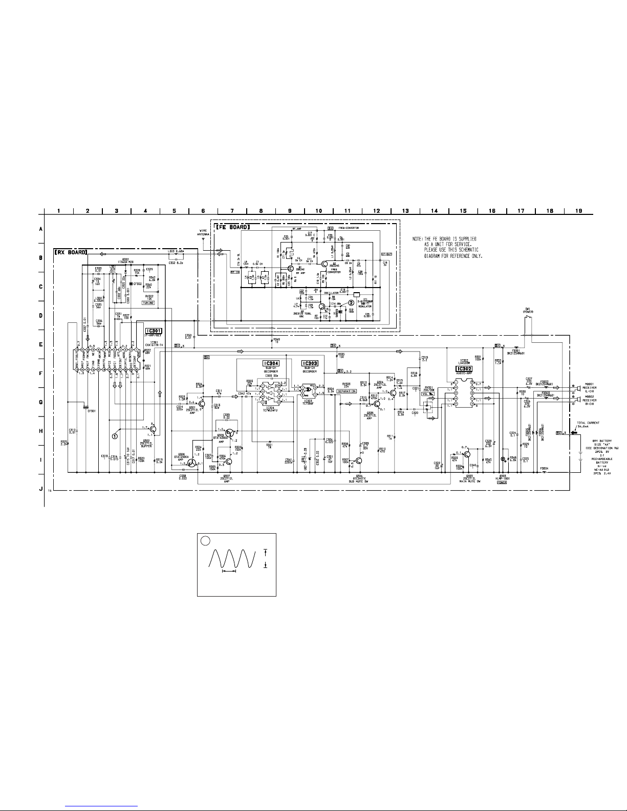
*A-4542-536-A FE BOARD, COMPLETE
******************
************************************************************
*A-4542-535-A RX BOARD, COMPLETE
******************
< CAPACITOR >
C301 1-124-589-11 ELECT 47uF 20% 16V
C302 1-164-489-11 CERAMIC CHIP 0.22uF 10% 16V
C303 1-162-921-11 CERAMIC CHIP 33PF 5% 50V
C306 1-164-227-11 CERAMIC CHIP 0.022uF 10% 25V
C307 1-162-927-11 CERAMIC CHIP 100PF 5% 50V
C309 1-126-572-11 ELECT 4.7uF 20% 35V
C310 1-110-563-11 CERAMIC CHIP 0.068uF 10% 16V
C311 1-162-923-11 CERAMIC CHIP 47PF 5% 50V
C312 1-162-970-11 CERAMIC CHIP 0.01uF 10% 25V
C313 1-162-926-11 CERAMIC CHIP 82PF 5% 50V
C314 1-162-957-11 CERAMIC CHIP 220PF 5% 50V
C315 1-124-233-11 ELECT 10uF 20% 16V
C316 1-164-245-11 CERAMIC CHIP 0.015uF 10% 25V
C317 1-162-970-11 CERAMIC CHIP 0.01uF 10% 25V
C318 1-164-346-11 CERAMIC CHIP 1uF 16V
C319 1-164-505-11 CERAMIC CHIP 2.2uF 16V
C320 1-164-346-11 CERAMIC CHIP 1uF 16V
C321 1-164-346-11 CERAMIC CHIP 1uF 16V
C322 1-124-242-00 ELECT 33uF 20% 25V
C324 1-107-725-11 CERAMIC CHIP 0.1uF 10% 16V
C325 1-107-725-11 CERAMIC CHIP 0.1uF 10% 16V
C326 1-124-635-00 ELECT 220uF 20% 6.3V
C327 1-124-635-00 ELECT 220uF 20% 6.3V
C328 1-124-635-00 ELECT 220uF 20% 6.3V
C329 1-164-346-11 CERAMIC CHIP 1uF 16V
C330 1-162-964-11 CERAMIC CHIP 0.001uF 10% 50V
C331 1-162-912-11 CERAMIC CHIP 7PF 0.5PF 50V
C332 1-164-441-11 CERAMIC CHIP 68PF 5% 50V
C333 1-163-021-91 CERAMIC CHIP 0.01uF 10% 50V
C334 1-124-233-11 ELECT 10uF 20% 16V
C335 1-162-924-11 CERAMIC CHIP 56PF 5% 50V
C336 1-162-924-11 CERAMIC CHIP 56PF 5% 50V
C337 1-162-970-11 CERAMIC CHIP 0.01uF 10% 25V
C338 1-163-037-11 CERAMIC CHIP 0.022uF 10% 25V
C339 1-164-489-11 CERAMIC CHIP 0.22uF 10% 16V
C340 1-164-346-11 CERAMIC CHIP 1uF 16V
C341 1-162-966-11 CERAMIC CHIP 0.0022uF 10% 50V
C342 1-162-923-11 CERAMIC CHIP 47PF 5% 50V
C350 1-163-021-91 CERAMIC CHIP 0.01uF 10% 50V
C352 1-162-198-31 CERAMIC 8.2PF 10% 50V
C355 1-162-919-11 CERAMIC CHIP 22PF 0.5PF 50V
< FILTER >
CF301 1-577-588-11 FILTER, CERAMIC
CF302 1-567-163-11 FILTER, CERAMIC
< DIODE >
D301 8-719-045-99 DIODE RD2.2M-T1B
D302 8-719-002-81 DIODE 1T363
D303 8-719-066-57 LED SA2512 (POWER)
< FERRITE BEAD >
FB301 1-414-234-11 INDUCTOR CHIP 0UH
FB302 1-414-234-11 INDUCTOR CHIP 0UH
FB303 1-414-234-11 INDUCTOR CHIP 0UH
FB304 1-414-234-11 INDUCTOR CHIP 0UH
FB305 1-414-234-11 INDUCTOR CHIP 0UH
FB306 1-414-234-11 INDUCTOR CHIP 0UH
< IC >
IC301 8-752-066-93 IC CXA1611N-T4
IC302 8-759-802-75 IC LA4533M
IC303 8-759-195-02 IC TC7S86F-TE85L
IC304 8-759-096-87 IC TC7WU04FU(TE12R)
< JUMPER RESISTOR >
JC301 1-216-296-91 SHORT 0
JC302 1-216-296-91 SHORT 0
JC303 1-216-296-91 SHORT 0
JC304 1-216-296-91 SHORT 0
JC305 1-216-296-91 SHORT 0
JC308 1-216-864-11 METAL CHIP 0 5% 1/16W
JC309 1-216-295-91 SHORT 0
JC310 1-216-864-11 METAL CHIP 0 5% 1/16W
JC312 1-216-295-91 SHORT 0
JC313 1-216-864-11 METAL CHIP 0 5% 1/16W
JC314 1-216-864-11 METAL CHIP 0 5% 1/16W
JC315 1-216-864-11 METAL CHIP 0 5% 1/16W
JC316 1-216-295-91 SHORT 0
JC317 1-216-295-91 SHORT 0
< COIL >
L301 1-422-317-31 COIL, AIR-CORE
L302 1-412-933-11 INDUCTOR 0.33uH
L303 1-414-140-11 INDUCTOR 0.68uH
RXFE