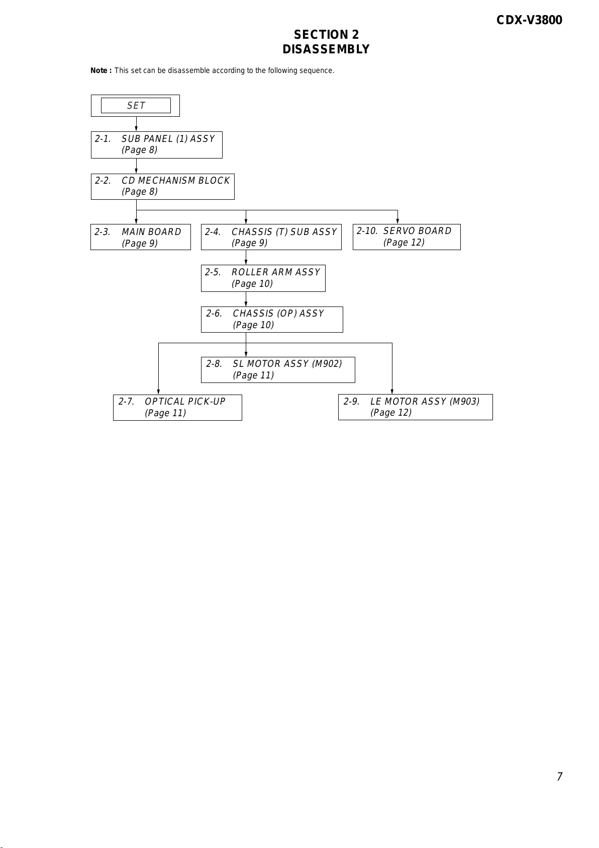
Sony CDX-V3800 User manual

1
Ver. 1.3 2006.05
Model Name Using Similar Mechanism NEW
CD Drive Mechanism Type MG-611MM-186//K
Optical Pick-up Name KSS1000E
SERVICE MANUAL
E Model
Chinese Model
CD player section
Signal-to-noise ratio 90 dB
Frequency response 10 – 20,000 Hz
Wow and flutter Below measurable limit
Signal format system PAL/NTSC
Tuner section
FM
Tuning range FM tuning interval:
50 kHz/200 kHz
switchable
87.5 – 108.0 MHz
(at 50 kHz step)
87.5 – 107.9 MHz
(at 200 kHz step)
Aerial terminal External aerial connector
Intermediate frequency 10.7 MHz/450 kHz
Usable sensitivity 9 dBf
Selectivity 75 dB at 400 kHz
Signal-to-noise ratio 67 dB (stereo),
69 dB (mono)
Harmonic distortion at 1 kHz
0.5% (stereo),
0.3% (mono)
Separation 35 dB at 1 kHz
Frequency response 30 – 15,000 Hz
AM
Tuning range AM tuning interval:
9 kHz/10 kHz switchable
531 – 1,602 kHz
(at 9 kHz step)
530 – 1,710 kHz
(at 10 kHz step)
Aerial terminal External aerial connector
Intermediate frequency 10.7 MHz/450 kHz
Sensitivity 30 µV
SPECIFICATIONS
Power amplifier section
Outputs Speaker outputs
(sure seal connectors)
Speaker impedance 4 – 8 ohms
Maximum power output 52 W ×4 (at 4 ohms)
General
Outputs Audio output terminals (front, rear/sub switchable)
Video output terminal
Power aerial relay control terminal
Power amplifier control terminal
Inputs AUX IN terminal
Parking break control terminal
Aerial input terminal
Tone controls Low:
±10 dB at 60 Hz (XPLOD)
Mid:
±10 dB at 1 kHz (XPLOD)
High:
±10 dB at 10 kHz (XPLOD)
Power requirements 12 V DC car battery
(negative earth)
Dimensions Approx. 178 ×50 ×179 mm (w/h/d)
Mounting dimensions Approx. 182 ×53 ×161 mm (w/h/d)
Mass Approx. 1.2 kg
Supplied accessories Parts for installation and connections (1 set)
Front panel case (1)
Card remote commander RM-X158
Design and specifications are subject to change without
notice.
• The tuner and CD sections have no adjustments.
Sony Corporation
eVehicle Division
Published by Sony Techno Create Corporation
9-879-406-04
2006E04-1
© 2006.05
FM/AM MULTI MEDIA PLAYER
CDX-V3800

2
CDX-V3800
CAUTION
Use of controls or adjustments or performance of procedures
other than those specified herein may result in hazardous
radiation exposure.
SAFETY-RELATED COMPONENT WARNING!!
COMPONENTS IDENTIFIED BY MARK 0OR DOTTED LINE
WITH MARK 0ON THE SCHEMATIC DIAGRAMS AND IN
THE PARTS LIST ARE CRITICAL TO SAFE OPERATION.
REPLACE THESE COMPONENTS WITH SONY PARTS WHOSE
PART NUMBERS APPEAR AS SHOWN IN THIS MANUAL OR
IN SUPPLEMENTS PUBLISHED BY SONY.
NOTES ON HANDLING THE OPTICAL PICK-UP BLOCK
OR BASE UNIT
The laser diode in the optical pick-up block may suffer electrostatic
breakdown because of the potential difference generated by the
charged electrostatic load, etc. on clothing and the human body.
During repair, pay attention to electrostatic breakdown and also use
the procedure in the printed matter which is included in the repair
parts.
The flexible board is easily damaged and should be handled with
care.
NOTES ON LASER DIODE EMISSION CHECK
The laser beam on this model is concentrated so as to be focused on
the disc reflective surface by the objective lens in the optical pick-
up block. Therefore, when checking the laser diode emission, ob-
serve from more than 30 cm away from the objective lens.
Notes on Chip Component Replacement
•Never reuse a disconnected chip component.
•Notice that the minus side of a tantalum capacitor may be dam-
aged by heat.
SERVICE NOTES
If the optical pick-up block is defective, please replace the whole
optical pick-up block.
Never turn the semi-fixed resistor located at the side of optical
pick-up block.
TEST DISCS
This set can playback CD-R and CD-ROM discs. The following
test discs should be used to check the capability:
CD-R test disc TCD-R082LMT (Part No. J-2502-063-1)
CD-RW test disc TCD-W082L (Part No. J-2502-063-2)
optical pick-up
semi-fixed resistor
This label is located on the bottom of the chassis.
Ver. 1.2
E model
Chinese model

3
CDX-V3800
Notes on CD-Rs (recordable CDs)/CD-RWs (rewritable
CDs)
This unit can play the following discs:
Type of discs Label on the disc
Audio CD
MP3 files
•Some CD-Rs/CD-RWs (depending on the equipment used for
its recording or the condition of the disc) may not play on this
unit.
•You cannot play a CD-R/CD-RW that is not finalized∗.
•You can play MP3 files recorded on CD-ROMs, CD-Rs, and
CD-RWs.
•A CD-R/CD-RW to which a session can be added can be played.
∗A process necessary for a recorded CD-R/CD-RW disc to be
played on the audio CD player.
Notes on Video CDs
This unit can play the following discs:
Type of discs Label on the disc
Video CD
VCD
A compact disc that contains moving pictures.
The picture data uses the MPEG 1 format (Video CD), worldwide
standards of digital compression technology.
Video CDs also contain compact audio data.
Sounds outside the range of human hearing are compressed while
the sounds we can hear are not compressed.
zUNLEADED SOLDER
Boards requiring use of unleaded solder are printed with the lead
free mark (LF) indicating the solder contains no lead.
(Caution: Some printed circuit boards may not come printed with
the lead free mark due to their particular size.)
: LEAD FREE MARK
Unleaded solder has the following characteristics.
• Unleaded solder melts at a temperature about 40°C higher than
ordinary solder.
Ordinary soldering irons can be used but the iron tip has to be
applied to the solder joint for a slightly longer time.
Soldering irons using a temperature regulator should be set to
about 350°C.
Caution: The printed pattern (copper foil) may peel away if the
heated tip is applied for too long, so be careful!
•Strong viscosity
Unleaded solder is more viscous (sticky, less prone to flow)
than ordinary solder so use caution not to let solder bridges
occur such as on IC pins, etc.
•Usable with ordinary solder
It is best to use only unleaded solder but unleaded solder may
also be added to ordinary solder.

4
CDX-V3800
TABLE OF CONTENTS
1. GENERAL
Location of Controls................................................................ 5
Connections ............................................................................. 5
2. DISASSEMBLY
2-1. Sub Panel (1) Assy .............................................................. 8
2-2. CD Mechanism Block ......................................................... 8
2-3. Main Board ......................................................................... 9
2-4. Chassis (T) Sub Assy .......................................................... 9
2-5. Roller Arm Assy ................................................................ 10
2-6. Chassis (OP) Assy ............................................................. 10
2-7. Optical Pick-up ................................................................. 11
2-8. SL Motor Assy (M902) .....................................................11
2-9. LE Motor Assy (M903)..................................................... 12
2-10. Servo Board....................................................................... 12
3. DIAGRAMS
3-1. Block Diagram –CD Section–........................................... 13
3-2. Block Diagram –Main Section–........................................ 14
3-3. Block Diagram –Display Section–.................................... 15
3-4. Circuit Boards Location .................................................... 15
3-5. Printed Wiring Boards –CD Mechanism Section–............ 17
3-6. Schematic Diagram –CD Mechanism Section (1/2)– ....... 18
3-7. Schematic Diagram –CD Mechanism Section (2/2)– ....... 19
3-8. Printed Wiring Boards –Main Section– ............................ 20
3-9. Schematic Diagram –Main Section (1/3)– ........................ 21
3-10. Schematic Diagram –Main Section (2/3)– ........................ 22
3-11. Schematic Diagram –Main Section (3/3)– ........................ 23
3-12. Printed Wiring Board –Display Section– .......................... 24
3-13. Schematic Diagram –Display Section–............................. 25
4. EXPLODED VIEWS
4-1. Main Section ..................................................................... 32
4-2. Front Panel Section ........................................................... 33
4-3. CD Mechanism Section (1) ............................................... 34
4-4. CD Mechanism Section (2) ............................................... 35
4-5. CD Mechanism Section (3) ............................................... 36
4-6. CD Mechanism Section (4) ............................................... 37
5. ELECTRICAL PARTS LIST......................................... 38

5
CDX-V3800
SECTION 1
GENERAL This section is extracted
from instruction manual.
CONNECTIONS
4
Location of controls
Refer to the pages listed for details.
aVolume +/– button
bATT (attenuate) button 17
cDSPL (display mode change) button
11, 14
dOPEN/EJECT shutter 11, 12
eDisplay window
fEQ3 button 18
gOFF (Stop/Power off) button*
1
10, 12,
18
hSEEK +/– button
Radio:
To tune in stations automatically/find a
station manually.
CD/VCD:
To skip tracks/fast-forward, reverse a track.
i(front panel release) button 10
jSOURCE (Power on/Radio/CD/AUX)
button
To select the source.
kMODE button
To change the operation.
lSEL (select) button
To select items.
mRESET button (located on the front side of
the unit, behind the front panel) 9
nNumber buttons 17
Radio:
To store stations/receive stored stations.
CD/VCD:
(1): REP 15
(2): SHUF 15
(3): SLOW 13
(4): AUDIO 14
(5): OSD 19
(6): PAUSE 12, 13
oFrequency select switch (located on the
bottom of the unit)
See “Frequency select switch” in the
Installation/Connections manual.
pSENS/ALBUM – button 12, 16
qBTM/ALBUM + button 12, 15
rSCRL (scroll) button 14
sReceptor for the card remote
commander
*1 Warning when installing in a car without an
ACC (accessory) position on the ignition switch
After turning off the ignition, be sure to press and
hold (OFF) on the unit until the display disappears.
Otherwise, the display does not turn off and this causes
battery drain.
EQ3
AT T OFF
SOURCE MODE SEL
SEEK
123456
SENS
SLOW
–
ALBUM
+
AUDIO OSD PAUSEREP SHUF
CDX-V3800
BTM SCRL
DSPL
5
The corresponding buttons of the card
remote commander control the same
functions as those on this unit.
aOFF button
bSOURCE button
cPBC button 14
dENTER button 14
e<(.)/,(>) buttons
fDSPL button
gVOL (+/–) button
hATT button
iSEL button
jMODE button
kO(return) button 14
lM(+)/m (–) buttons 14
mSCRL button
nNumber buttons
Note
If the display disappears by pressing
(OFF)
, it cannot
be operated with the card remote commander unless
(SOURCE)
on the unit is pressed, or a disc is inserted
to activate the unit first.
Tip
For details on how to replace the battery, see
“Replacing the lithium battery” on page 20.
Selecting an album with the card
remote commander
Album can be skipped using M(+)/m (–) on the
card remote commander.
*
Available only when an MP3 file is played.
Skipping tracks continuously
Press once <or ,on the card remote
commander, then press again within 2 seconds
and hold.
Card remote commander RM-X158
OFF
DSPL
REP SHUF SLOW
PBC
SCRL
SOURCE
SEL MODE
PA U S EOSDAUDIO
132
465
AT T
VOL
+
–
+
–
ENTER
2
3
9
1
qd
4
5
6
8
7
qf
qa
qs
q;
To Press
Skip albums*
–Albumselection Mor m[once for each
album]
To continuously skip
albums, press and hold
either button.
2
A
B
AUDIO
OUT REAR
AUDIO OUT FRONT
VIDEO OUT

6
CDX-V3800

7
CDX-V3800
SECTION 2
DISASSEMBLY
Note : This set can be disassemble according to the following sequence.
2-1. SUB PANEL (1) ASSY
(Page 8)
2-2. CD MECHANISM BLOCK
(Page 8)
SET
2-3. MAIN BOARD
(Page 9) 2-4. CHASSIS (T) SUB ASSY
(Page 9)
2-5. ROLLER ARM ASSY
(Page 10)
2-6. CHASSIS (OP) ASSY
(Page 10)
2-8. SL MOTOR ASSY (M902)
(Page 11)
2-10. SERVO BOARD
(Page 12)
2-7. OPTICAL PICK-UP
(Page 11) 2-9. LE MOTOR ASSY (M903)
(Page 12)

8
CDX-V3800
2-2. CD MECHANISM BLOCK
Note : Follow the disassembly procedure in the numerical order given.
2-1. SUB PANEL (1) ASSY
2
two claw
s
3
two claws
4
sub panel (1) assy
1
two
screws
(+PTT 2.6
x
6)
8
bracket (CD)
6
CD mechanism block
SERVO board
4
CN751 (26core)
5
CN401
(2P)
3
1
screw
(+PTT 2.6
x
6
)
2
screw
(+PTT 2.6
x
6)
7
two
screws
(+PTT 2.6
x
6)

9
CDX-V3800
2-4. CHASSIS (T) SUB ASSY
2-3. MAIN BOARD
5
SENSOR board
6
chassis (T) sub assy
4
claw
3
claw
1
two
screws
(+P 1.7
x
2.2)
2
two
screws
(+P 1.7
x
2.2)
1
three screws
(+BTT )
3
MAIN board
4
insulating sheet
2
two
screws
(+PTT 2.6
x
8)
5
screw
(+PTT 2.6
x
8)
6
connection (video out) cor
d

10
CDX-V3800
2-5. ROLLER ARM ASSY
2-6. CHASSIS (OP) ASSY
4
gear (RA1)
5
roller arm assy
1
spring (RAL)
2
spring (RAR)
3
washer (1.1-2.5)
4
washer
0
coil spring (damper)
9
two coil springs (damper)
qa
chassis (OP) assy
5
gear (LE1)
1
CN500 (16P)
lever (D)
slider (R)
6
7
8
2
Remove the six solderings.
3
tension coil spring (KF60)

11
CDX-V3800
2-7. OPTICAL PICK-UP
2-8. SL MOTOR ASSY (M902)
1
screw
(+P 1.4
x
1.8)
2
SL motor assy (M902)
1
tension coil spring (CHKG
)
2
chucking arm sub assy
3
screw
(+B 1.4
x
5)
4
rack (SL)
5
claw
6
main shaft
7
optical pick-up

12
CDX-V3800
2-9. LE MOTOR ASSY (M903)
2-10. SERVO BOARD
2
washer
4
qd
3
gear (LE1)
7
leaf spring (LE)
5
lever (D)
bracket (LEM-N)
slider (R)
6
screw
(+P 1.7
x
2.2)
8
screw
(+M 1.7
x
2.5)
qa
screw
(+M 1.7
x
2.5)
qf
two toothed lock
screws
(+M 1.4
)
qs
screw
(+M 1.7
x
2.5)
9
bearing (LEB-N)
0
gear (LE) assy
qg
LE motor assy
(M903)
1
Remove the two solderings.
4
CN500 (16P)
6
claw
7
SERVO board
5
precision
screw
(+P 1.7
x
2.2)
2
Remove the eight solderings.
1
shield sheet
3
Remove the three solderings.

13 13
CDX-V3800
CDX-V3800
RF AMP,
DIGITAL SERVO,
IC500
52
EQ0
9
FEO
46
TZCRFM
48
TEO
51 RFI
8FEN
49 TEN
42 XI
43 XO
PD1
PD2
E
F
I-V AMP
PD LD
DETECTOR
35
DOUTA 96 CD DATA
36
LRCK 97 CD LRCK
34
WFCK 50 BATTLOW
37
DCK 98 CD BCLK
38
EFLAG 102 CD XCK
31
SUBSYQ 81 SUBSYQ
30
BUSY 80 BUSY
29
RESETX 82 XRESET
28
R/W 83 R/W
27
DIN/OUT 84 DI/DO
26
MCK 85 MCK
CLKIN
CLKIO
3
2
5
6
E
AC
BD
F
13 LD 12
PD
24
LON
(FOCUS)
(TRACKING)
2-AXIS DEVICE
OPTICAL
PICK-UP BLOCK
(KSS1000E)
• Siganal Path
: CD PLAY
LASER DIODE
M
M
M
17
18
14
13
12
11
10
9
VOL(+)
VOL(-)
FWD
REV
1
28
IN1(–) 3
OUT1
IN2(–)
OUT2
IN3(–)
OUT3
IN4(–)
OUT4
4
22 CLV OUT
6
7
18 TDOUT
17 JUMP0
23
19 SDIN
22
21 FD OUT
26
25
16
15
VO4(–)
VO4(+)
VO3(+)
VO3(-)
VO1(+)
VO1(-)
VO2(+)
VO2(-)
M903
(LOADING)
M901
(SPINDLE)
M902
(SLED)
FOCUS/TRACKING COIL DRIVE,
SLED/SPINDLE/LOADING
MOTOR DRIVE
IC600
CD-L MAIN
SECTION
A
56
VSYNC
36
DQMO
LDON
UDQM
WE
CAS
RAS
BA
CLK
14
9 15
WE B
10 16
CAS B
11 17
RASO B
112 19
BAO
SI
127 35
RAMCLK
55
HSYNC
78
AU LRCK
79
AU BCK
76
AU XCK
103
DEEMP
77
AU DATA
55 CD SELFSW
92 CD INSW
93 CD LOAD
CD SO
CD ON
BU+3.3V U COM+3.3V
1990
SO 91
SCK 93
RESET B 99
SP 88
MP 89
MUTE 113
16M SDROM
IC200
16M SDROM
IC300
VIDEO SIGNAL
PROCESSOR
IC400
DIGITAL SIGNAL PROCESSOR
IC100
DIGITAL
MODULATOR
IC700
CD SI
18
CD SCK
20
CD XRST
98
SP
54
MP
90
SW2
(SELF)
95 CD DSW
SW1
(DOWN)
S901
(LIMIT)
SW3
(DISC IN)
94 EJECT
69
CLK27 OUT
70
PLA NTSC
54
V RST
2DIN
1LRCK
3BCKIN
14 SCKI
12 DEEMP
9
LOUT
6
ROUT R-CH
10
MUTE
13
FORMAT
32
CVBS/Y
PD2
E
F
LD
MONOUT
FCS+
FCS–
TRK+
TRK–
PD1
AUTOMATIC
POWER
CONTROL
Q501
LASER ON
CONTROL
SWITCH
Q502
• R-ch is omitted due to same as L-ch.
66
65
X401
27MHz
X541
16.934MHz
MUTE
D701
MAIN
SECTION
B
15 CLK
14 MODEB
28 VSYNC
29 HSYNC
9SLEEP
YC0
I
YC7
P0
I
P7
27•25•23•21•22
•24•26•28
ROMD0
I
ROMD7
29–32•34•38•40•42
•41•39•33•35•44•
43•45–49
ROMA0
I
ROMA18
29•31•33•35
•38•30•42–44
DQ0
I
DQ7
45•25–18•
8–1•48•17
A0
I
A18
ROMA0-ROMA18
ROMD0-ROMD7
RAMA0-RAMA10
RAMD0-RAMD15
17–20•16–12
•111•110
DA0
I
DA10
21–24•
27–32•20
A0
I
A10
116–123•6–2
•126–124
2•3•5•6•8•
9•11•12•39•
40•42•43•45
•46•48•49
DQ0
I
DQ15
92 LIMIT
64
I
57
17
I
24
20 SD OUT
87
CN401
(VIDEO OUT)
114
DD0
I
DD15
SYSTEM CONTROL
IC801 (1/3)
CD POWER
CONTROL
Q701,703
3-1. BLOCK DIAGRAM — CD SECTION —
(Page 14)
(Page 14)
SECTION 3
DIAGRAMS

1414
CDX-V3800
CDX-V3800
3-2. BLOCK DIAGRAM — MAIN SECTION —
1ANT 7B2
ELECTRONIC VOLUME
IC401
PJ601
(ANTENNA)
TUX601
(TUNER UNIT)
POWER AMP
IC100
SYSTEM CONTROL
IC801 (2/3)
CNP901
6B1
R-CH (FRONT)
R-CH (REAR)
BATT
9C2
8C1
R-CH
4
3
10
VCC
11
TU VDD
15
E2P VDD
13
TU-SCL
14
TU-SDA
6
S-METER
7
TU MUTE
16
E2P SCL
17
E2P SDA
45 VSM
AU+8V
TU+5V
U COM+3.3V
15 TU ATT
25 EEP SCK
24 EEP SIO
L
R
CD-L
R-CH
17
18
OUTS2
OUTS1 R-CH
L
R
5
3
LF+
LF-
9
7
RF+
RF-
29
27
SW1
R-CH
SW2
BATT
30
37
REG1
REG2
31
33
REG3
REG4
34
REG5
TU+5V
BATT
25
24
OUTF1
OUTR1
29
MUTE
2SDA
AU+8V
U-COM+3.3V
SERVO+3.3V
MECHA+6V
DISP+B
4SCL
SDA
SCL
16 ACGND
22 STB
25 DIAG
AU+8V
35 VP
15
7
10
12
11
16
1
9
2
4
3
5
6
30
31
SCL
SDA
SCL
SDA
SCL
SDA
SCL
SDA
33
IIC SCK
34
IIC SIO
6
VOL ATT
1
LINE ATT
5
BEEP
31
STB
56
DIAG
53
BU IN
67
PAK BK
12 IN RR(FL) FL+
FL-
RL+
RL-
FR+
FR-
RR+
RR-
AMP-REM
ANT-REM
ACC
PAK BK
23
OUTF2
11 IN RF(RL)
22
OUTR2
MUTE
Q405
MUTE
Q407
REAR
AUDIO OUT
MUTE DRIVE
Q400,401
58
UNI SI
59
UNI SO
64
ACC IN ACC CHECK
Q900
TU+5V REG
Q601
BATT
BATTERY CHECK
Q902
BACK-UP
DETECT
Q906,907
MUTE
Q404
D400
D702
F900
R-CH
L
R
FRONT
AUDIO OUT
R-CH
5
3
AP2
AP1 R-CH
L
R
AUX IN
PJ401
D912
BATT
D915
CD
SECTION A
MUTE CD
SECTION
B
BATT
• Signal Path
• R-CH is omitted due to same as L-CH.
: CD PLAY
: FM
: AM
(Page 13)
(Page 13)

15 15
CDX-V3800
CDX-V3800
3-3. BLOCK DIAGRAM — DISPLAY SECTION —
ACK ON
SWITCH
Q800
X801
32.768kHz
79
80
82
83
38
28
29
27
39
47
75
77
LCD DRIVER
IC501
KEYIN0
CLK
CE
LCD SO
LCD SCK
LCD CE
DIMMER
KEYIN1
KEY ACK
46 DST SEL
XKEY ON
46 DST SEL
RESET
DOOR SW
2IN 1
OUT
X1A
X0A
X0
X1
X800
18.432MHz
S802
RESET
S800
9K
10K
FREQUENCY
SELECT
63
64
62
1
LCD501
LIQUID
CRYSTAL
DISPLAY
PANEL
LED501,502
LCD
BACK LIGHT
D801
S522
(OPEN)
3
I
50
•
51
I
54
|
SEG3
SEG50
COM4
COM1
|
CL
DI
CE
DISP+B
65
SIRCS IR
LED504-518,
520-522,524,525
2OUT
U COM+3.3V
()
KEY MATRIX
S501-521,523
26
SYSTEM CONTROL
IC801 (3/3)
IR RECEIVER
IC502
SHUT SW
LED
CONTROL
Q502
72
RESET
IC802
DISPLAY
BOARD
DIMMER
3-4. CIRCUIT BOARDS LOCATION
MAIN board
DISPLAY board
SENSOR board
SERVO board
SPEAKER board
tuner unit
(TUX601
)

1616
CDX-V3800
CDX-V3800
• NOTE FOR PRINTED WIRING BOARDS AND SCHEMATIC DIAGRAMS
THIS NOTE IS COMMON FOR PRINTED WIRING
BOARDS AND SCHEMATIC DIAGRAMS.
(In addition to this, the necessary note is printed
in each block.)
For schematic diagrams.
Note:
•All capacitors are in µF unless otherwise noted. (p: pF)
50 WV or less are not indicated except for electrolytics
and tantalums.
•All resistors are in Ωand 1/4W or less unless otherwise
specified.
•f: internal component.
•C: panel designation.
For printed wiring boards.
Note:
•X: parts extracted from the component side.
•Y: parts extracted from the conductor side.
•a: Through hole.
•: Pattern from the side which enables seeing.
(The other layers' patterns are not indicated.)
•A: B+ Line.
•Voltages and waveforms are dc with respect to ground
under no-signal (detuned) conditions.
• CD mechanism section (1/2, 2/2)
no mark : CD PLAY
•Main (1/3), (2/3), (3/3) and Display sections
no mark : FM
():AM
<>:CD PLAY
∗: Impossible to measure
•Voltagesare taken witha VOM (Input impedance 10MΩ).
Voltage variations may be noted due to normal produc-
tion tolerances.
•Waveforms are taken with a oscilloscope.
Voltage variations may be noted due to normal produc-
tion tolerances.
•Circled numbers refer to waveforms.
•Signal path.
J: CD PLAY
F: FM
f: AM
Caution:
Pattern face side: Parts onthe patternfaceside seenfrom the
(Side B) pattern face are indicated.
Parts face side: Parts on the parts face side seen from the
(Side A) parts face are indicated.
Q
C
These are omitted
EB
EThese are omitted
CB
CThese are omitted
BE
Note: The components identified by mark 0or dotted line
with mark 0are critical for safety.
Replace only with part number specified.
• WAVEFORMS
1
IC801 i; (XOA)
32.768 kHz
3.6 Vp-p
18.432 MHz
2
IC801 is (X0)
4.1 Vp-p
0.2 V/DIV, 20
µ
sec/DIV
0.5 V/DIV, 0.1
µ
sec/DIV
1
IC500 rd (XO)
16.9344 MHz
1.8 Vp-p
2
IC500 ts (EQO)
0.2 V/DIV, 0.2
µ
sec/DIV
0.5 V/DIV, 0.5
µ
sec/DIV
27 MHz
3
IC100 yg (CLKIN)
1.5 Vp-p
0.2 V/DIV, 0.2
µ
sec/DIV
0.8 V to
1.3 Vp-p
— Servo Board — (MODE: CD PLAY) — Main Board —
Ver. 1.3

17 17
CDX-V3800
CDX-V3800
1
A
B
C
D
E
F
G
H
I
23456789101112 13 14 15
SW3
SW2
TP63
TP64
TP57
TP58
TP61
TP62
TP59
TP60 BP1
BP2
BP3
TP551
TP552
TP553
TP554
TP555
TP556
TP557
TP558
TP559
TP560
TP561 TP562TP563
TP564
TP51 TP52
TP542
TP501
TP503
TP504
TP603
TP601
TP621
C704
C702
C701
TP622
BP4
FMB3
FMB4
FMB5
TP23
TP22
TP21
TP19
TP17
TP18
TP16
TP15
TP14
TP13
TP11
TP10
TP2
TP1
TP5
TP4
TP20
TP6
TP3
C703
TP56
TP53
TP55
FMB6
TP513
TP512
TP522
TP519
TP531 TP529
TP527
TP528
TP530
TP523
TP524
TP525
TP521
TP24
TP12 TP8
TP9
C101
X541
TP541
CN500
C505
C707
C544
RB109
C545
C503
C504
C542
C546
C502
RB108
C551
C541
C543
R165
R170
R172
R176
R551
R506
R546
R707
R604
R543
R501
R502
R545
R171
R173
R177
R602
R503
R504
R505
C506
R541
R600
R622
R701
R702
R703
R704
IC500
R625
R544
C400
C547
C548
C705
C103
C600
C531
R542
C706
C165
C160
CN1
IC700
FB501
C517
Q502
C501
C518
R547
C507
C512
R515
C516
R511
C405
C521
C515
R516
R514
R513
RB301
R512
R630
R104
R105
R628
R312
R311
R403
C513
C508
C514
C301
C302
C202
IC200
CN401
C511
D908
D910
D906
C520
C510
C519
C509
R708
R631
FB503
FB502
R548
C540
L101
TP181
TP182 TP183
TP184
TP185
TP186
TP187
TP131
FMA3
FMA4
C623
C603
C159
IC101
C601
C621
TP188
TP189
RB101
RB102
RB103
RB104
RB105
RB106
RB107
RB110
RB111
C605
C163
RB113
C406
C407
RB112
C180
R508
R509
R163
R166
R168
R180
R404
R709
R601 R603
R621
R624
R167
R169
R175
R181
R507
C162
C112
R106
R107
R108
R161
R162
R109
R110
R111
SW1
R112
R113
R114
R627
R164
C102
C708
R632
D101
Q501
C709
C183
C182
C181
C164
C161
C132
R178
X401
C166
IC100
C111
IC600
R405
C304
C305
C312
C313
C402
C403
C404
R401
R402
R101
R102
R103
C410
R629
L401
C201
C131
C303
IC300
IC400
C401
C408
D907
D909
C133
FB504
R605
R606
R623
R626
3-5. PRINTEDWIRING BOARDS — CD MECHANISM SECTION — • Refer to page 15 for Circuit Boards Location. : Uses unleaded solder.
(Page 20)
Ref. No. Location
D101 G-3
D906 B-11
D907 B-2
D909 B-1
D910 F-9
IC100 E-3
IC200 B-11
IC300 B-3
IC400 C-2
IC500 D-10
IC600 H-2
IC700 G-10
Q501 E-5
Q502 E-9
• Semiconductor
Location

1818
CDX-V3800
CDX-V3800
• Refer to page 16 for Waveforms.
3-6. SCHEMATIC DIAGRAM — CD MECHANISM SECTION (1/2) — • Refer to page 26 for IC Block Diagrams. • Refer to page 27 for IC Pin Description of IC500.
IC B/D
IC B/D
IC B/D
BP3
BP4
BP2
BP1
TP60
CN500
C505
C540
C605
C544
C545
C503
C504
C542
C541
R551
R546
R621
R624
R543
R545
R505
C506
TP57
R600
R622
TP551
TP552
TP553
TP554
TP555
TP556
TP557
TP558
TP559
TP560
TP561
TP562
TP563
TP564
TP51
TP52
TP503
TP504
TP501
TP502
TP541
TP542
TP601
TP603
TP621
TP622
TP63
TP61
TP58
TP59
TP62
TP64
C705
C531
CN1
C518
C507
C512
C516
C521
C515
R516
R512
C513
TP55
TP53
TP511
TP56
C514
C511
C708
C510
R623
C519
R626
R509 R508
R507
R506
C707
C502
R547
R542
R511
R513
R514
R515
R603
R604
R602R601
FB501
R544
C543
R606
R605
C600
R627
C551
R708
C501
C508
M901
M902
M903
S901
SW3
SW2
SW1
Q501
IC600
IC500
IC700
C517
Q502
R625
C546
R709
C709
R707
C706
C509
C547 C548
X541
R541
R548
R632
D910
R501
R502
R503
R504
TP519
TP531
TP522
TP526
TP525
TP521
TP524
TP528
TP530
TP527
TP523
TP529
TP513
TP512
TP5
TP1
TP2
TP20
TP4
TP6
TP3
TP10
TP8
TP12
TP9
TP11
TP13
TP14
TP15
TP18
TP16
TP17
TP7
TP19
TP21
TP22
TP23
TP24
(Page 19)
(Page 23)
Ver. 1.3

19 19
CDX-V3800
CDX-V3800
• Refer to page 16 forWaveform.
3-7. SCHEMATIC DIAGRAM — CD MECHANISM SECTION (2/2) — • Refer to page 26 for IC Block Diagram. • Refer to page 29 for IC Pin Description of IC400.
IC B/D
BP7
R163
R165
C112
R164
TP131
TP181
TP185
TP187
TP188
TP189
C102
C182
C181
C164
C132
X401
C111
C304
C305
C312
C313
C402
C403
C404
C405
R403 TP401
TP402
C301
L401
C302
C202
C131
C303
CN401
C401
C103
R162
R176
RB107
R312
R311
R112
R113
R114
R111
R109
R110
R629
R404
R402
C183
TP186
TP183
TP182
TP184
R102
R101
C165
C180
R180
C162
C166
C163
C161
C160
R401
CN401
D101
IC100
FB503
IC400
FB502
IC300
RB111
RB110
RB106
RB105
RB104
RB103
RB102
RB101
RB112
R630
R631
RB301
RB113
R181
R405
C407
C406
R161
C133
FB504
IC200
C201
C410 D907
C400
D906
D909
R178
R702
R703
R704
R172
R170
R168
R166
R701
R167
R169
R171
R173
R175
R177
R106
R107
R108
R103
R104
R105
RB109
RB108
(Page 18)

2020
CDX-V3800
CDX-V3800
1
A
B
C
D
E
F
G
H
I
J
234567891011 12 13 14
JW204 JW205
JW206
JW207
5678
1234
JW203
JW200
JW202
JW201
R843
R849
R850
D902
C420
C423
C422
R421
C421
R420
R417
R416
R415
R414
R442
R407
R406
R405
R404
R413
R408
C113
R418
R412
D600
R424
R402
R403
C409
D400
C408
Q601
Q404
Q402
Q401
D301
R419
Q403
R606
R607
R608
R834
R832
R705
JR10
D702
JR12
R839
R840
R841
R847
R846
R702
C709
R813
D912
D915
Q902
R931
C443
Q701
R828
R409
R830
IC801
D918
Q405
R823
R822
R821
R801
D802
R804
R916
R806
C807
FB702
D701
C816
C817
R835
R836
Q900
R903 R902
R443
C612
R805
R800
FB902
R817
R816
R927
R819
R936
C992
C433
C434
C435
C436
R411
R430
C620
Q400
R809
R701
R441
D801
R860
R901
R818
R810
R440
R436
R435
L703
C614
R615
Q703
R848
R837
Q407
R703
R709
R437
L602
Q406
R925
D808
Q800
C451
JR5
C450
R468 R708
D903
R814
R873
C812
R302
D825
C437
IC802
R425
C440
C444
R427
R428
R432
Q906
C438
R932
R913
D914
C303
R448
C441
C446
R447
R426
C821
C822
R824
R825
R826
FB901
C815
R904
C706
Q907
C991
JR6
C990
FMB3
FMB4
C994
R853
R854
IC401
C993
C439
R812
D823
L400
C416
D916
JW39
D922
JW85
S800
JW59
JW107
JW105
JW111
JW100
C705
JW95
C106
C813
JW123
C411
JW122
C424
C428
D917
JW117
JW52
JW37
C414
JW77
C413
C412
JW56
C410
R429
JW14
CNP901
F901
IC100
PJ401
JW110
JW41
JW10
JW106 JW99
JW93
JW91
X801
JW19
C447
JW104
JW68
JW55
JW98
JW109
JW108
C922
JW67
JW115
JW86
JW49
JW66
JW63
JW120
JW28
JW65
JW92
D921
JW62
JW24
JW83
JW103
D919
JW70
JW34
JW5
JW78
JW60 L701
L702
C707
JW84
C704
C809
L900
JW127
JW36
X800
C810
JW45
JW22
JW20
JW79
JW128
C908
R604
C701
JW6
JW119
JW134
JW8
R845
C101
R917
JW50
L700
JW47
R603
JW82
R400
JW42
JW31
JW35
JW141
JW61
CN751
JW30
JW94
JW51
JW113
JW72
JW140
JW80
R928
JW69
JW124
JW27
TUX601
JW151
R833
JW116
JW76
JW11
JW114
JW97
JW3
C619
D907
JW102
JW18
JW145
JW144
JW9
JW73
JW38
JW131
JW96
JW75
C426
JW64
C425
C453
C452
JW43
JW48
JW143
D908
JW101
S802
S802
RESET
JW29
JW130
C111
JW74
C107
D906
JW121
JW12
PJ601
C825
R401
JW54
CNP800
DISPLAY BOARD
CN901
SERVO
BOARD
CN1
JW46
C109
R815
JW126
JW150
C618
D909
R431
JW44
C711
R912
C430
JW13
D820
C454
JW40
C417
JW112
JW17
JW125
JW15
JW142
JW118
JW25
JW1
JW2
JW4
JW58
1-865-780-
11
1-865-781-
11
S800
FREQUENCY
SELECT
D905
D904
D817
D813
D816
D814
D812
D811
D815
3-8. PRINTEDWIRING BOARDS — MAIN SECTION — • Refer to page 15 for Circuit Boards Location. : Uses unleaded solder.
(Page 17)
(Page 24)
D301 E-2
D400 D-4
D600 E-2
D701 G-7
D702 G-6
D801 I-6
D802 I-5
D808 J-9
D811 I-3
D812 I-3
D813 I-3
D814 I-2
D815 I-2
D816 I-2
D817 I-2
D820 I-4
D823 J-4
D825 J-4
D902 B-7
D903 B-8
D904 C-6
D905 C-6
D906 C-7
D907 C-7
D908 C-7
D909 C-7
D912 E-10
D914 C-9
D915 E-10
•Semiconductor Location
Ref. No. Location D916 C-8
D917 C-8
D918 C-9
D919 D-9
D921 D-6
D922 C-6
IC100 B-6
IC401 F-4
IC801 H-7
IC802 H-10
Q400 D-4
Q401 D-4
Q402 C-4
Q403 D-3
Q404 C-3
Q405 C-3
Q406 C-3
Q407 C-3
Q601 E-2
Q701 F-10
Q703 F-10
Q800 I-6
Q900 H-10
Q902 F-10
Q906 G-10
Q907 G-10
Ref. No. Location
Other manuals for CDX-V3800
2
Table of contents
Other Sony Media Player manuals

Sony
Sony YY1298B User manual

Sony
Sony Network Walkman NW-E403 User manual

Sony
Sony DVP-NW50 - In-wall Dvd Player User guide

Sony
Sony NW-MS9 SonicStage v2.0 User manual

Sony
Sony HAP-S1 User manual

Sony
Sony NW-A105 User manual

Sony
Sony Walkman NWZ-E453K User manual

Sony
Sony LocationFree LF-B10 User manual

Sony
Sony J-1 User manual

Sony
Sony NW-ZX707 Reference guide