Sony SMP-N100 User manual

Sony Corporation
Home Entertainment Business Group
SERVICE MANUAL
9-890-736-11
2010G6900-1
© 2010.07
Published by Design Engineering Dept.
NETWORK MEDIA PLAYER
Ver. 1.0 2010.07
SMP-N100
RMT-D301
SPECIFICATIONS
US Model
Canadian Model
AEP Model
UK Model
Wireless
Wireless LAN standard:
IEEE802.11/b/g/n (Except Russian)
Frequency range:
US:
2.4GHz band: Channels 1-11
CANADIAN:
AEP, UK, RUSSIAN:
General
Supplied accessor ies
Specifications and design are subject to change
without notice.
1 Photo : SMP-N100
Remote : RMT-D301
Russian Model
Inputs and outputs
(Jack name:
Jack type/Output level/Load impedance)
LINE OUT R-AUDIO-L:
Phono jack/2 Vrms/10 kilohms
DIGITAL OUT (OPTICAL):
Optical output jack/–18 dBm
(wave length 660 nm)
HDMI OUT:
HDMI 19-pin standard connector
COMPONENT VIDEO OUT
(Y, P B, P R):
Phono jack/Y: 1.0 Vp-p/
PB, PR: 0.7 Vp-p/75 ohms
LINE OUT VIDEO:
Phono jack/1.0 Vp-p/75 ohms
LAN (100):
100BASE-TX Terminal
USB:
USB jack Type A (For connecting a USB
memory, hard disk drive, memory card
reader, digital still camera, and digital video
camera)
Power requirements:
AC adapter: 110 – 240 V AC, 50/60 Hz
Power consumption (approx.):
14 W
Dimensions (approx.):
185 mm × 193 mm × 40 mm
(17 3/8in. × 7 5/8in. × 1 5/8in.)
(width/depth/height) incl. projecting parts
Mass (approx.):
680 g (1 lb 8 oz)
Operating temperature:
5 ºC to 35 ºC (41 °F to 95 °F)
Operating humidity:
25 % to 80 %
Modulation:
DS-SS Modem and OFDM Modem
DC IN:
12 V DC
•Audio/video cable (phono plug ×3) (1)
•AC power cord (1)
•AC adapter (1)
•Remote control (remote) (1)
•Size AA (R6) batteries (2)
*Except Russian
*Russian ONLY
IEEE802.11/b/g (Russian ONLY)
2.4GHz band: Channels 1-11
2.4GHz band: Channels 1-13

– 2 –
SMP-N100
SAFETY CHECK-OUT
LEAKAGE TEST
The AC leakage from any exposed metal part to earth ground and
from all exposed metal parts to any exposed metal part having a
return to chassis, must not exceed 0.5 mA (500 microamperes).
Leakage current can be measured by any one of three methods.
1. A commercial leakage tester, such as the Simpson 229 or RCA
WT-540A. Follow the manufacturers' instructions to use these
instruments.
2. A battery-operated AC milliammeter. The Data Precision 245
digital multimeter is suitable for this job.
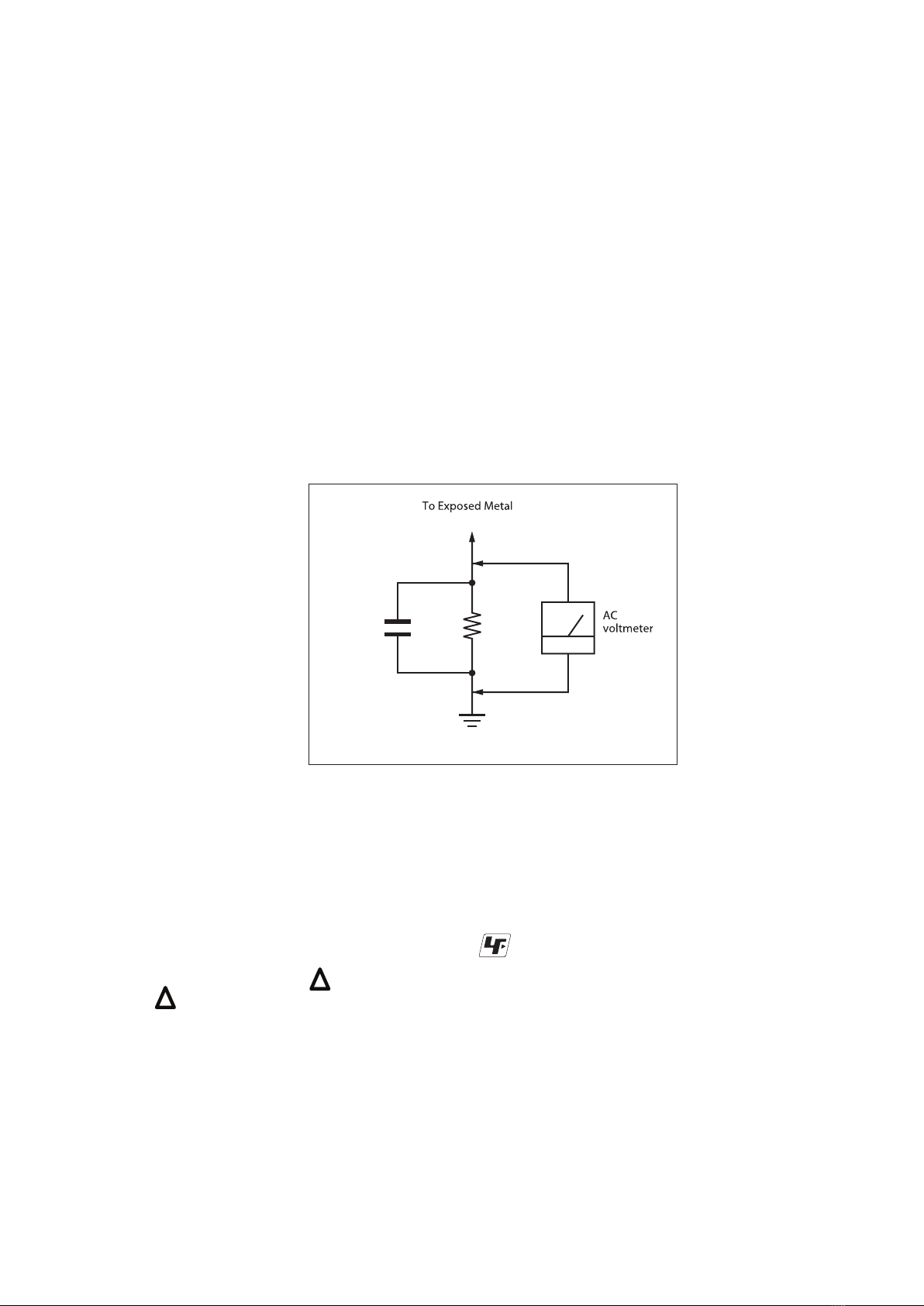
3. Measuring the voltage drop across a resistor by means of a
VOM or battery-operated AC voltmeter. The “limit” indication
is 0.75V, so analog meters must have an accurate low-voltage
scale. The Simpson 250 and Sanwa SH-63Trd are examples of a
passive VOM that is suitable. Nearly all battery operated digital
multimeters that have a 2V AC range are suitable. (See Fig. A)
1. Check
the area of your repair for unsoldered or poorly-soldered
connections. Check the entire board surface for solder splashes
and bridges.
2. Check the interboard wiring to ensure that no wires are “pinched”
or contact high-wattage resistors.
3. Look for unauthorized replacement parts, particularly transistors,
that were installed during a previous repair. Point them out to
the customer and recommend their replacement.
4. Look for parts which, though functioning, show obvious signs
of deterioration. Point them out to the customer and recommend
their replacement.
5. Check the line cord for cracks and abrasion. Recommend the
replacement of any such line cord to the customer.
6. Check the B+ voltage to see it is at the values specified.
7. Check the antenna terminals, metal trim, “metallized” knobs,
screws, and all other exposed metal parts for AC leakage. Check
leakage as described below.
After correcting the original service problem, perform the following
safety checks before releasing the set to the customer:
1.5k
Ω
0.15µF(0.75 V)
Parts on Set
Earth Ground
Fig. A. Using an AC voltmeter to check AC leakage.
Unleaded solder
Boards requiring use of unleaded solder are printed with the lead-
free mark (LF) indicating the solder contains no lead.
(Caution: Some printed circuit boards may not come printed with
the lead free mark due to their particular size.)
: LEAD FREE MARK
Unleaded solder has the following characteristics.
•Unleaded solder melts at a temperature about 40°C higher than
ordinary solder.
Ordinary soldering irons can be used but the iron tip has to be
applied to the solder joint for a slightly longer time.
Soldering irons using a temperature regulator should be set to
about 350°C.
Caution: The printed pattern (copper foil) may peel away if the
heated tip is applied for too long, so be careful!
•Strong viscosity
Unleaded solder is more viscous (sticky, less prone to flow) than
ordinary solder so use caution not to let solder bridges occur such
as on IC pins, etc.
•Usable with ordinary solder
It is best to use only unleaded solder but unleaded solder may
also be added to ordinary solder.
WARNING!!
WHEN SERVICING, DO NOT APPROACH THE LASER
EXIT WITH THE EYE TOO CLOSELY. IN CASE IT IS
NECESSARY TO CONFIRM LASER BEAM EMISSION,
EROMFOECNATSIDAMORFEVR
ESBOOTERUSEB
THAN 25 cm FROM THE SURFACE OF THE OBJEC-
TIVE LENS ON THE OPTICAL PICK-UP BLOCK.
SAFETY-RELATED COMPONENT WARNING!!
COMPONENTS IDENTIFIED BY MARK ENILDETTODRO
WITH MARK NIDNASMARGAIDCITAMEHCSEHTNO
THE PARTS LIST ARE CRITICAL TO SAFE OPERATION. RE-
ESOHWSTRAPYNOSHTIWSTNENOPMOCESEHTECALP
ROLAUNAMSIHTNINWOHSSARAEPPASREBMUNTRAP
IN SUPPLEMENTS PUBLISHED BY SONY.
ATTENTION AU COMPOSANT AYANT RAPPORT
À LA SÉCURITÉ!
LES COMPOSANTS IDENTIFIÉS PAR UNE MARQUE 0
ETSILALTESEUQITAMÉHCSSEMMARGAIDSELRUS
EDÉTIRUCÉS
ALRUOPSEUQITIRCTNOSSECÈIPSED
STNASOPMOCSECRECALPMEREN.TNEMENNOITCNOF
TNOSSORÉMUNSELTNODYNOSSECÈIPSEDRAPEUQ
DONNÉS DANS CE MANUEL OU DANS LES SUPPLÉ-
MENTS PUBLIÉS PAR SONY.
!
!

– 3 –
TABLE OF CONTENTS
1. SERVICE NOTE
1-1. USB HARNESS DRESSING
1-1-1 Keep distance the USB Harness from the Heatsink ... 1-1E
SMP-N100
Section Title Page
1-1-2 Keep distance the USB Harness from the
Upper Chassis ............................................................. 1-1E
2. DISASSEMBLY
2-1 TOP COVER ASSY .................................................... 2-1
2-2 MB-136 Board, FL200 and WLAN Card ................... 2-2E
2-3 Circuit Boards Location ............................................ 2-2E
3. BLOCK DIAGRAMS
3-1 OVERALL BLOCK DIAGRAM .................................. 3-1
3-2 DSP BLOCK DIAGRAM ........................................... 3-2
3-3 AV OUT BLOCK DIAGRAM ...................................... 3-3
3-4 USB/ETHER/WLAN BLOCK DIAGRAM ................... 3-4
3-5 POWER BLOCK DIAGRAM ..................................... 3-5E
4. SCHEMATIC DIAGRAMS
4-1 This Note Is Common For Schematic Diagrams ........ 4-1
4-2 FRAME SCHEMATIC DIAGRAM ............................. 4-2
4-3 FL-200 BOARD (FRONT CONNECTOR)
SCHEMATIC DIAGRAM ........................................... 4-3
4-4 MB-136 BOARD (CXD9983GG/9984GG)
SCHEMATIC DIAGRAM (1/15) ................................ 4-4
4-5 MB-136 BOARD (CXD9983GG/9984GG)
SCHEMATIC DIAGRAM (2/15) ................................ 4-5
4-6 MB-136 BOARD (POWER1)
SCHEMATIC DIAGRAM (3/15) ................................ 4-6
4-7 MB-136 BOARD (CLK/POWER2)
SCHEMATIC DIAGRAM (4/15) ................................ 4-7
4-8 MB-136 BOARD (FLASH/HOST)
SCHEMATIC DIAGRAM (5/15) ................................ 4-8
4-9 MB-136 BOARD (USB)
SCHEMATIC DIAGRAM (6/15) ................................ 4-9
4-10 MB-136 BOARD (HDMI)
SCHEMATIC DIAGRAM (7/15) .............................. 4-10
5. PRINTED WIRING BOARDS
5-1 THIS NOTE IS COMMON FOR
PRINTED WIRING BOARDS .................................... 5-1
5-2 FL-200 (POWER SWITCH)
PRINTED WIRING BOARDS ..................................... 5-2
5-3 MB-136 BOARD (MAIN)
PRINTED WIRING BOARDS (SIDE A) ..................... 5-3
5-4 MB-136 BOARD (MAIN)
PRINTED WIRING BOARDS (SIDE B) .................... 5-4E
6. IC PIN FUNCTION DESCRIPTION ............. 6-1
7. SERVICE MODE ............................................. 7-1
8. ERROR LOG LIST ......................................... 8-1
9. TROUBLESHOOTING ................................... 9-1
10. REPAIR PARTS LIST10-1. EXPLODED VIEWS
10-1 EXPLODED VIEWS .............................................. 10-1
10-1-1 MAIN SECTION .................................................... 10-1
10-1-2 ACCESSORIES .................................................... 10-2
10-2 ELECTRICAL PARTS LIST ................................... 10-3
4-11 MB-136 BOARD (SATA)
SCHEMATIC DIAGRAM (8/15) ............................... 4-11
4-12 MB-136 BOARD (AUDIO)
SCHEMATIC DIAGRAM (9/15) .............................. 4-12
4-13 MB-136 BOARD (VIDEO)
SCHEMATIC DIAGRAM (10/15) ............................ 4-13
4-14 MB-136 BOARD (GPIO/JTAG)
SCHEMATIC DIAGRAM (11/15) ............................ 4-14
4-15 MB-136 BOARD (ETHERNET)
SCHEMATIC DIAGRAM (12/15) ............................. 4-15
4-16 MB-136 BOARD (FE_POWER/SF/SATA)
SCHEMATIC DIAGRAM (13/15) ............................. 4-16
4-17 MB-136 BOARD (FE_OP/MOTOR DRIVE)
SCHEMATIC DIAGRAM (14/15) ............................ 4-17
4-18 MB -136 BOARD (IFCON )
SCHEMATIC DIAGRAM (15/15) ............................ 4-18
4-19 WAVEFORMS ..................................................... 4-19E
Section Title Page

1-1E
SMP-N100
SECTION 1
SERVICE NOTE
1-1. USB HARNESS DRESSING
USB-017: 1-967-372-11
1-1-1. Keep distance the USB Harness from the Heatsink
1-1-2. Keep distance the USB Harness from the Upper Chassis
Usethe Lead Pin to
bend down the
USB Harness to
avoid touching the
upper chassis
Keep the distance
between the USB
Harness and
Heatsink

2-1
SMP-N100
SECTION 2
DISASSEMBLY
2-1. TOP COVER ASSY
+BV3 (3-CR)
Five screws
SCREW +P 3X3
Top Cover Assy
1
2
3One screw
Top Cover
5
4
Three screws
Note: Follow the disassembly procedure in the numerical order given.
+BV3 (3-CR)

2-2E
SMP-N100
2-2. MB-136 Board, FL-200 and WLAN Card
1
Five screws
4
MB-136 Board
6
FL-200 Board
Wireless LAN Card
5
One screw
7
Two screws
8
Flexible Flat Cable (MF-046)
2
Harness (USB-017)
3
2-3. Circuit Boards Location
FL-200 Board
WLAN Card
MB-136 Board
a
bb
+BV3 (3-CR)
+BV3 (3-CR)
+BV3 (3-CR)
a

FL-200 BOARD
Y
P
B
P
R
L
R
C
N1
2
0
1
L
A
N(1
0
0
)
I
C
1
20
1
E
T
HER
NET
P
HY
X1
2
0
1
25
M
H
Z
(AC IN)
A
3-1
SMP-N100
SECTION 3
BLOCK DIAGRAMS
3-1. OVERALL BLOCK DIAGRAM
The components identified by
mark or dotted line with mark
are critical for safety.
Replace only with part number
specified.
IC1003
VIDEO AMP
IC901
D/A CONVERTER
HUB
HDMI
USB
ETHERNET
VIDEO
AUDIO
(ANALOG OUTPUT)
(DIGITAL OUTPUT)
AUDIO
MB-136 BOARD
A-BUS
IC204
IC205
IC104
IC105
IC501
IC502
2G/16G NAND
FLASH
S-FLASH
16M
X401
27MHZ
X802
25MHZ
IC1504
P FAIL
IC1503
SUB SYSTEM
CONTROL
CN603
S3001
POWER
POWER-1
UNSW6V
A/C
ADAPTOR
IC2301
POWER
WIRELESS LAN CARD
(WLAN MODULE)
+5V
USB - WLAN
OPTICAL
CN701
HDMI OUT
AUDIO
LINE OUT
DIGITAL OUT
PCM/DTS/DOLBY
DIGITAL
IC904
OPTICAL
TRANSMITTER
VIDEO
COMPONENT
VIDEO OUT
J904
B-BUS
SATA I/F, MEMORY CONTROL,
A/V OUT, HDMI, ETHERNET I/F,
USB I/F
MAIN SYSTEM CONTROL, DSP
CXD9983GG/CXD9984GG
IC101
IC1501
USB
EXT
ANT-1
ANT-2
J301
4051NC

3-2
AU23
IC104
1Gb DDR2
SDRAM
X401
27MHZ
X802
25MHZ
IC101
MAIN SYSTEM CONTROL,
DSP,SATA I/F,MEMORY CONTROL
A/V OUT,HDMI,ETHERNET I/F
USB I/F,
AW23
A_RRASB
IC105
1Gb DDR2
SDRAM
DODQ0-DODQ15
DOA0-DOA12
A_RCASB
A_RWEB
A_RODT
A_RCLK0
A_RCLKB
A_RCLKE
A_RCSB
BB28, AU27,
AT28
A_RBA0
A_RBA1
A_RBA2
BB24
BA29
BC21
BC29
BA21
AV24
DODQ16-DODQ31
K3
K7
/CAS
/WE
ODT
CK
/CK
CKE
/CS
/RAS
L1 L-L3
BA0 - BA2
L7
K2
J8
K9
K8
L8
K3
K7
L1 L-L3
BA0 - BA2
L7
K2
J8
K9
K8
L8
MB-136 BOARD
/CAS
/WE
ODT
CK
/CK
CKE
/CS
/RAS
A_RCLK1
A_RCLK1B
BA39
BC39
IC204
1Gb DDR2
SDRAM
B_RRASB
IC205
1Gb DDR2
SDRAM
DIDQ0-DIDQ15
DIA0-DIA12
B_RCASB
B_RWEB
B_RODT
B_RCLK0
B_RCLK0B
B_RCLKE
B_RCSB
B_RBA0
B_RBA1
B_RBA2
AH40
AC41
AL43
AG41
AL41
AD42
DIDQ16-DIDQ31
K3
K7
/CAS
/WE
ODT
CK
/CK
CKE
/CS
/RAS
L1 L-L3
BA0 - BA2
L7
K2
J8
K9
K8
L8
K3
K7
L1 L-L3
BA0 - BA2
L7
K2
J8
K9
K8
L8
/CAS
/WE
ODT
CK
/CK
CKE
/CS
/RAS
B_RCLK1
B_RCLK1B
N41
N43
AC43
AJ41
A25
BB8
BA9
FE_RFIP
Y2
FE_RFIN
Y4
FE_RFIP2
W1
FE_RFIN2
W3
FE_INA
P2
FE_INB
N1
FE_INC
R3
FE_IND
T6
FE_INE
V6
FE_INF
U1
FE_ING
R1
FE_INH
T2
FE_TRAY_IN
FE_TRAY_OUT
FE_CFREQ
AD2
FE-CMOD
AE7
FE_FMO4
FE_FMO3
FE_GAINSW1
AF6
FE_FOO
AD4
FE_TRO
AH6
FE_TLO
A M 8
FE_LIM IT
AG3
FE_FMO
AE1
FE_FMO2
AF4
FE_DMD0
FE-OSCEN
AF8
M4
THERMO
AG7
AE5
FE_TRAYPWM
C25
AJ5
AK4
AE3
CPU_PRERST (2/2)
PAGE 3-4
IC502
16Mb
NOR -FLASH
7
5
2
6
1
F42
H40
G41
J39
IC501
16
18
8
CPU_NFD0 - CPU_NFD7
19
17
7
9
3-2. DSP BLOCK DIAGRAM
M38
K38
L37
G43
M36
P38
CPU_NFCEN
CPU_NFCLE
CPU_NFALE
CPU_NFWEN
CPU_NFREN
CPU_NFRBN
nCE
ALE
cLE
nRE
RY/BY
WE
CPU_XRST
PAGE 3-4
2Gb/16Gb
NAND FLASH
CPU_SFDO
CPU_SFDI
CPU_SFCK
CPU_SFCS
NS_XTALO
NSTAL25MI
NXTAL25MO
NS_XTALI
SI
SO
SCK
CS
,63DA,04DA
93CA
AF2
CXD9983GG/CXD9984GG
SMP-N100

CEC PULL-UP
ISOLATING SWITCH
V
I
D
E
OA
M
P
I
C
1
01
I
C
1
00
3
IC901
C3
3
B3
2
A3
3
7
5
3
1
8
1
4
D3
0
H1
4
G
1
5
Y
P
B
P
R
7
8
9
10
C2
3
E2
3
B2
2
D2
2
H2
0
A1
9
D2
6
B2
6
C2
7
A2
7
D2
8
C2
9
A2
9
G
3
9
B2
8
1
0
1
1
1
3
1
5
1
1
16
1
Y
I
N
P
BI
N
PRI
N
V
I
N
M
U
T
E
SD/
H
D
P
Y
O
U
T
P
B
O
U
T
PR
O
UT
VO
U
T
J9
0
4
L
R
I
C
9
04
O
P
T
I
C
A
L
T
RAN
S
M
I
TTE
R
T
X
2
P
1
3
4
6
7
9
1
0
1
2
1
9
1
3
CEC
IT-CON
Q702
PG 3-4
3-3. AV OUT BLOCK DIAGRAM
3-3
VIDEO
AUDIO
LINE OUT
COMPONENT
VIDEO OUT
OPTICAL
DIGITAL OUT
PCM/DTS/DOLBY
DIGITAL
CN701
D/A CONVERTER
AOUTL
AOUTR
XMUTE
DACDAT
LRCK
BCLK
MCLK
D901
IFCON_XMUTE
DAC3.3VA
TX2N
TX1P
TX1N
TX0P
TX0N
TXKP
TXKN
TMDS DATA2+
TMDS DATA2-
TMDS DATA1+
TMDS DATA1-
TMDS DATA0+
TMDS DATA0-
TMDS CLOCK+
TMDS CLOCK-
HPD
CEC
HDMI OUT
T
X
2
P
TX2N
TX1P
TX1N
TX0P
TX0N
TXKP
TXKN
CH2_P
CH2_M
CH1_P
CH1_M
CH0_P
CH2_M
CLK_P
CLK_M
HTPLG
SPDIF
AMUTE
AOMCK
AOBCK
AOLRCK
AOSDATA0
VIND8
VIND6
DACOUT6
FORMAT1
XVMUTE
CVBS
Y
PB
PR
DACOUT1
DACOUT3
DACOUT2
LORTNOCYROMEMF/IATAS
F/ITENREHTEIMDH,TUOV/A
F/IBSU GG4899DXC/GG3899DXC
PSD,LORTNOCMETSYSNIAM
XAMUTE
MB-136 BOARD
SMP-N100

MB-136 BOARD
CN1102
CN1502
X1201
25MHz
IC1201
10
R
LAN (100)
C43
D40
D42
E39
D38
F36
B38
C41
A43
H34
A41
B40
C39
A39
C37
F38
E37
B42
3
2
B34
G33
A35
C19
D34
A17
E35
AV12
A14
3
1
C35
Front end circuit
MRESET
C35
CPU_PRERST
CPU_PRERST 2
1
GPIO2
GPIO1
CORE_RESETB
GPIO6
VSTB
GPIO4
GPIO5
A37
D36
AW11
AY10
3
1
48
2
3
4
5
47
46
49
KEY0
2
3
4
5
KEY0
CN1201
3-4. USB/ ETHER/ WLAN BLOCK DIAGRAM
3-4
GG4899DXC/GG3899DXC
2
3
2
3
CN603
DP
DM
IC1503
11
34
CN1504
USB
WIRELESS
LAN CARD
(WLAN
MODULE)
S3001
CN3001
FL-200 BOARD
SMP-N100
FRONT
ETHERNET
1 1
IC3001
D3001
POWER
D3002
WLAN

3-5. POWER BLOCK DIAGRAM
SMP-N100
3-5E
UNSW12V
DCDC6V
3.8V
1ch
DCDC
M
T8530
D
D
R2_1.8V
D
DR2_VTT0. 9V
3.3V
D
D
R2_1. 8V
CORE_STB3. 3V
CO
RE_1.1V
D
D
R2
× 4
REG
1.8V
0.9V
効率90%
REG 1.2V
CPU_3. 3VA
1ch
DCDC
1ch
DCDC
VTT REG
1.1V
CPU
_1.2VA
12V 3.8V
3.8V
12V
12V
3.3V
3.8V REG HD
M
I_3. 3V
PCONT_2
IC308 IC307
D
AC3.3V
5.8V 3.3V
IC305
REG
IC303
H
D
M
I_1.2V
IC704
IC309
PCONT_CORE
0.9V
VREF_0. 9V
IC310
IC311
( Back End)
PCONT_3
PCONT_3
PCONT_3
PCONT_3
PCONT_3
D
CD
C4V
I C101
PCONT_3
3.3VA
1. 2VA
5V H
D
M
I5V
REG
5.8V HDM
I
H
ot Plug
U
SB5V
U
SB5V
REG 5V
5.8V
5V
U
SB
REG IF-CO
N I C1503
3.3V
3.3VA Fl as h
G
PIO
JTAG
5.8V
12V
IC705
REG
IC314
IC601
IC602
PCONT_3
USB_VBUS_PCONT1
USB_VBUS_PCONT2
Et herPHY
CORE_STB3.3V (= 3.3VA)
Ether_3.3V
WLAN
REG
REG
VI D
EO_Buf f er 3. 3V
3.3V3.8V
-5V-6V
Audi o
D
AC/ AM
P
IC901
VideoBuffer
IC1003
VI D
EO_Buf f er- 5V
DAC3.3V
IC1001
IC1002
PCONT_3
PCONT_2
AudioD
AC_3.3V
O
PTICAL
IC904
3.3VA
UNSW12V
UNSW3.3V
t o FL200
PS1501
FCC20 501AJ
PS301
DC JACK
UNSW12V
1ch
DCDC
FHC20 322AJ
IC312
PCONT_2
J301
DCDC-6V
1ch
DCDC
PS302
FCC20 102AJ
IC313
UNSW 3.3V
3-5E

4-1
SMP-N100
SECTION 4
SCHEMATIC DIAGRAMS
•All capacitors are in µF unless otherwise noted. pF : µµF.
50V or less are not indicated except for electrolytics and tantalums.
•All resistors are in ohms, 1/4 W (Chip resistors : 1 /10 W) un-less
otherwise specified.
kΩ=1000Ω, MΩ=1000kΩ.
•% : indicates tolerance.
•Caution when replacing chip parts.
New parts must be attached after removal of chip.
Be careful not to heat the minus side of tantalum capacitor, because
it is damaged by the heat.
•Constants of resistors, capacitors, ICs and etc with XX indicate
that they are not used.
In such cases, the unused circuits may be indicated.
•All variable and adjustable resistors have characteristic curve B,
unless otherwise noted.
• : nonflammable resistor
• : fusible resistor
• : panel designation
• f : internal component.
• : adjustment for repair.
• : B+ Line
• : B– Line
•Circled numbers refer to waveforms.
•Voltages are dc between measurement point.
•Readings are taken with a color-bar signals on Blu-ray disc.
•Readings are taken with a digital multimeter (DC 10MΩ).
•Voltage variations may be noted due to normal production toler-
ances.
Note:
The components identified
by mark or dotted line with
mark are critical for safety.
Replace only with part num-
ber specified.
Note:
Les composants identifiés par
une marque sont critiques
pour la sécurité.
Ne les remplacer que par une
pièce portant le numéro spécifié.
When indicating parts by reference number, please include the
board name.
4-1. THIS NOTE IS COMMON FOR SCHEMATIC DIAGRAMS

4-2
SMP-N100
1
A
B
C
D
E
F
G
H
I
28765
43
4-2. FRAME SCHEMATIC DIAGRAM
CN701
MB-136
CN1201
TO ETHERNET
FL-200
CN3001 8P
8P CN1504
5P CN601
CNXXX 5P
WLAN CARD
CN603 4P
USB-017
1-967-372-11
HARNESS
MF-049
1-838-208-11
FFC
TO HDMI
TO USB
SIRCS
GND
GND
LED 2
LED 1
KEY 0
USW 3.3V
USW 12V
SIRCS
GND
GND
LED 2
LED 1
KEY 0
USW 3.3V
USW 12V

4-3
SMP-N100
4-3. FL-200 BOARD (FRONT CONNECTOR) SCHEMATIC DIAGRAM
- Ref. No.: FL-200 board; 20,000 series -
• See page 5-2 for printed wiring board.
A
XX MARK:NO MOUNT
1
B
FL-200 BOARD
432
C
1
2
3
4
5
6
7
8
VS
OUT
GND
S3001
XX
R3001
C3002
10
6.3V
C3003
0.1
16V
470
1/10W
R3002
470
1/10W
R3003
CN3001
8P
C3001
XX
XX
R3004
XX
R3005
XX
R3006
JL3001
JL3002
JL3003
JL3004
JL3005
JL3006
JL3007
JL3008
100
R3007
Q3001
UNR52A5G0LS0
Q3002
UNR52A5G0LS0
IC3001
HM2140RS T-07M2
3D 001
MS L 1M- 3 8TTP 6
D3002
SML-M13PTT86
GND
UNSW3.3V
KEY0
LED1
LED2
GND
SIRCS
UNSW12V
WLAN_LED(GREEN)
LED(GREEN)
5

4-4
SMP-N100
1
A
B
C
D
E
F
G
H
I
J
212 13
11
10
98765
43 14
4-4. MB-136 BOARD (CXD9983GG/9984GG) SCHEMATIC DIAGRAM (1/15) •See page 5-3 for printed wiring board.
- Ref. No.: MB-136 board; 10,000 series
A SIDE
B SIDE

4-5
SMP-N100
1
A
B
C
D
E
F
G
H
I
J
212 13
11
10
98765
43 14
4-5. MB-136 BOARD (CXD9983GG/9984GG) SCHEMATIC DIAGRAM (2/15) •See page 5-3 for printed wiring board.
- Ref. No.: MB-136 board; 10,000 series
A SIDE
B SIDE

4-6
SMP-N100
1
A
B
C
D
E
F
G
H
I
J
212 13
11
10
98765
43 14
4-6. MB-136 BOARD (POWER1) SCHEMATIC DIAGRAM (3/15) •See page 5-3 for printed wiring board.
- Ref. No.: MB-136 board; 10,000 series

4-7
SMP-N100
1
A
B
C
D
E
F
G
H
I
J
212 13
11
10
98765
43 14
4-7. MB-136 BOARD (CLK/POWER2) SCHEMATIC DIAGRAM (4/15) •See page 5-3 for printed wiring board.
- Ref. No.: MB-136 board; 10,000 series

4-8
SMP-N100
1
A
B
C
D
E
F
G
H
I
J
212 13
11
10
98765
43 14
4-8. MB-136 BOARD (FLASH/HOST) SCHEMATIC DIAGRAM (5/15) •See page 5-3 for printed wiring board.
- Ref. No.: MB-136 board; 10,000 series

4-9
SMP-N100
1
A
B
C
D
E
F
G
H
I
J
212 13
11
10
98765
43 14
4-9. MB-136 BOARD (USB) SCHEMATIC DIAGRAM (6/15) •See page 5-3 for printed wiring board.
- Ref. No.: MB-136 board; 10,000 series
Other manuals for SMP-N100
5
Table of contents
Other Sony Media Player manuals

Sony
Sony NSP-100 Installation and operation manual

Sony
Sony NSP-1 User manual

Sony
Sony SMP-N200 User manual

Sony
Sony FMP-X1 User manual

Sony
Sony AZ-HS1 User manual

Sony
Sony DSX-A55BT User manual

Sony
Sony TEP-TX5 Instruction Manual

Sony
Sony NSZ-GU1 User manual

Sony
Sony Walkman NWZ-A826 User manual

Sony
Sony FMP-X5 User manual

Sony
Sony FMP-X1 User manual

Sony
Sony Network Walkman NW-HD3 User manual

Sony
Sony DSX-A400BT User manual

Sony
Sony HAP-Z1ES User manual

Sony
Sony CLIE PEG-N710C User manual

Sony
Sony HAP-S1 User manual

Sony
Sony FMP-X1 User manual

Sony
Sony NSZ-GX70 User manual

Sony
Sony LLS-201 User manual

Sony
Sony CLIE PEG-T665C Instruction sheet