–3 –
1. SERVICING NOTES
1-1. Notes on Handling the Optical Pick-up Block or Base Unit .. 4
1-2. Notes on Laser Diode Emission Check............................... 4
1-3. Notes on Chip Component Replacement ............................ 4
1-4. Flexible Circuit Board Repairing ........................................ 4
1-5. Chuck Plate Jig on Repairing .............................................. 4
1-6. Demonstration ..................................................................... 4
1-7. Checking the Laser Diode and Focus Search Operation..... 4
1-8. Jig for Checking BD Board Waveform ............................... 5
1-9. Checks Prior to Parts Replacement and Adjustments ......... 6
1-10. Change of Pulley .................................................................6
2. GENERAL
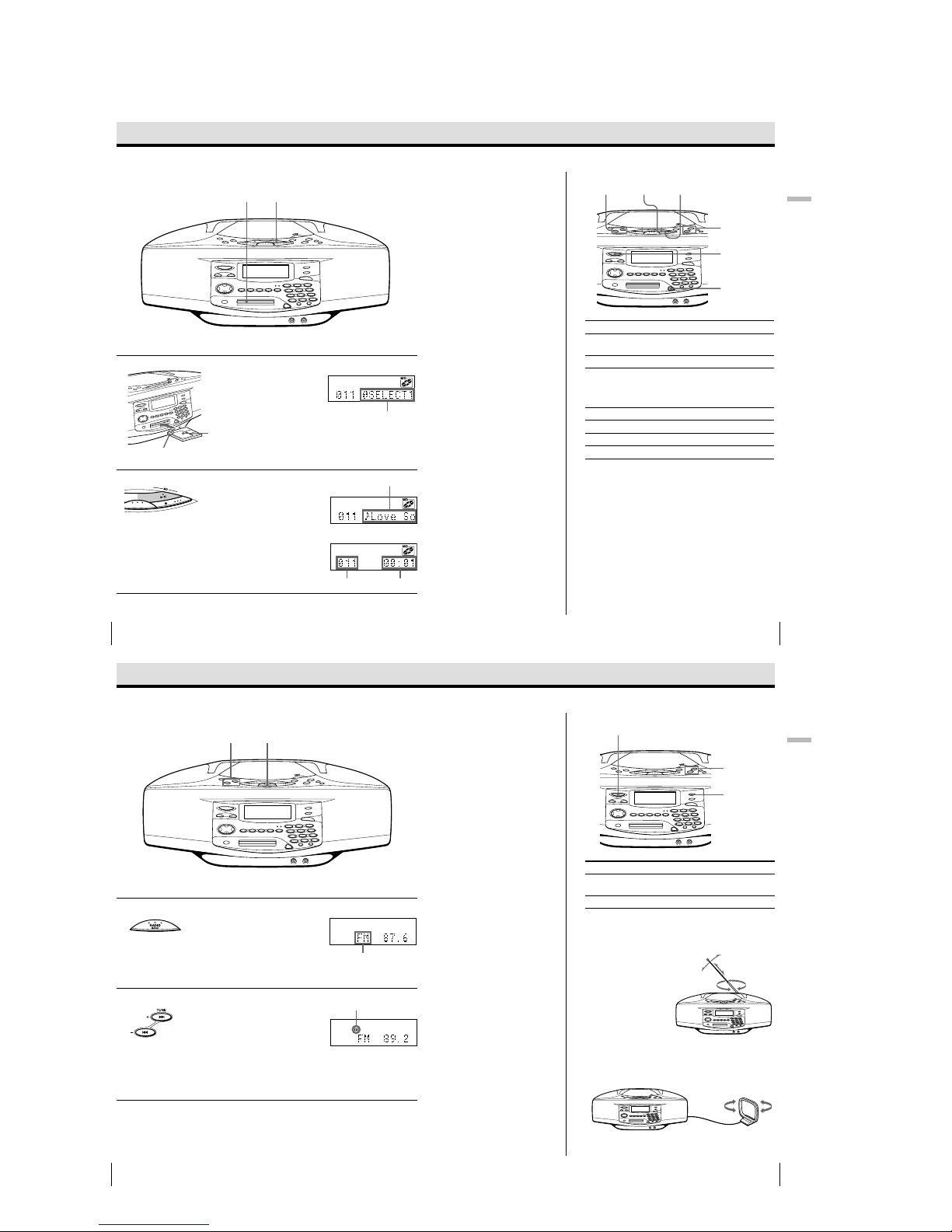
Playing a CD ....................................................................... 7
Recording a whole CD ........................................................ 7
Playing an MD..................................................................... 8
Listening to the radio........................................................... 8
3. DISASSEMBLY
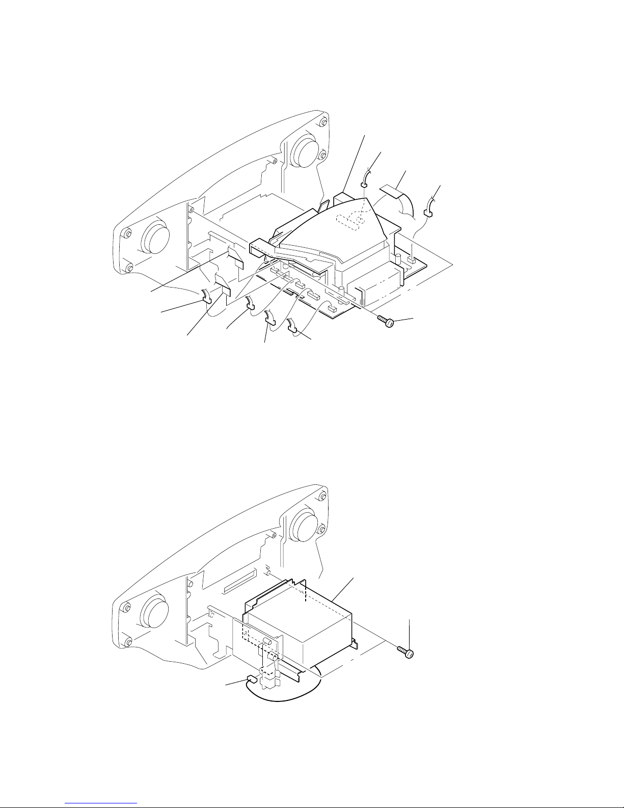
3-1. Cabinet (Rear) Assy ............................................................ 9
3-2. Power Board ........................................................................ 9
3-3. Cabinet (Upper) Assy ........................................................ 10
3-4. MD Block Assy ................................................................. 10
3-5. Tuner Board ....................................................................... 11
3-6. Jack Board ......................................................................... 11
3-7. LED Board ........................................................................ 12
3-8. Key Board ......................................................................... 12
3-9. Top Board .......................................................................... 13
3-10. FL Board ........................................................................... 13
3-11. Main board ........................................................................ 14
3-12. CD Board .......................................................................... 14
3-13. CD Mechanism Block .......................................................15
3-14. DG Board .......................................................................... 15
3-15. Plate (Front), Shield .......................................................... 16
3-16. MD Mechanism Block-1 (MDM-5GA) ............................16
3-17. MD Mechanism Block-2 (Slider (Cam) Assy) ................. 17
3-18. MD Mechanism Block-3 (BD Board)............................... 18
3-19. MD Mechanism Black-4 (SW Board)...............................18
4. TEST MODE
4-1. MD section ........................................................................ 19
5. ELECTRICAL ADJUSTMENTS
5-1. Tuner section ..................................................................... 22
5-2. MD section ........................................................................ 24
5-3. CD section ......................................................................... 31
TABLE OF CONTENTS
6. DIAGRAMS
6-1. IC Pin Function Descriptions ............................................33
6-2. Circuit Boards Location .................................................... 42
6-3. Block Diagram –Tuner Section– ....................................... 43
6-4. Block Diagram –MD Section–..........................................46
6-5. Block Diagram –CD Section–........................................... 49
6-6. Block Diagram –Audio Section– ......................................51
6-7. Schematic Diagram –CD Section (1/2)–...........................53
6-8. Schematic Diagram –CD Section (2/2)–...........................55
6-9. Printed Wiring Boards –CD Section– ...............................57
6-10. Printed Wiring Boards –Tuner Section– ........................... 59
6-11. Schematic Diagrams –Tuner Section– .............................. 61
6-12. Printed Wiring Boards –BD Section– ............................... 63
6-13. Schematic Diagram –BD Section (1/2)–...........................65
6-14. Schematic Diagrams –BD Section (2/2)– ......................... 67
6-15. Schematic Diagram –DG Section– ................................... 69
6-16. Schematic Diagram –DG Section– ................................... 71
6-17. Printed Wiring Board –DG Section–.................................73
6-18. Printed Wiring Board –Main Section– .............................. 75
6-19. Schematic Diagram –Main Section (1/3)– ........................ 77
6-20. Schematic Diagram –Main Section (2/3)– ........................ 79
6-21. Schematic Diagram –Main Section (3/3)– ........................ 81
6-22. Printed Wiring Boards –Panel Section– ............................83
6-23. Schematic Diagrams –Panel Section–............................... 85
6-24. Printed Wiring Boards –Switch Section–.......................... 87
6-25. Schematic Diagrams –Switch Section– ............................89
6-26. Printed Wiring Boards –Power Supply Section– .............. 91
6-27. Schematic Diagrams –Power Supply Section– .................93
6-28. IC Block Diagrams............................................................ 95
7. EXPLODED VIEWS
7-1. Cabinet (Rear) Section .................................................... 101
7-2. Cabinet (Front) Section ...................................................102
7-3. Cabinet (Upper) Section.................................................. 103
7-4. MD Block Section........................................................... 104
7-5. MD Mechanism Section (MDM-5GA) .......................... 105
7-6. MD Base unit Section (MBU-5A) ................................. 106
7-7. Optical Pick-up Section (KSM-213CDM)...................... 107
8. ELECTRICAL PARTS LIST.................................... 108


 User manual")