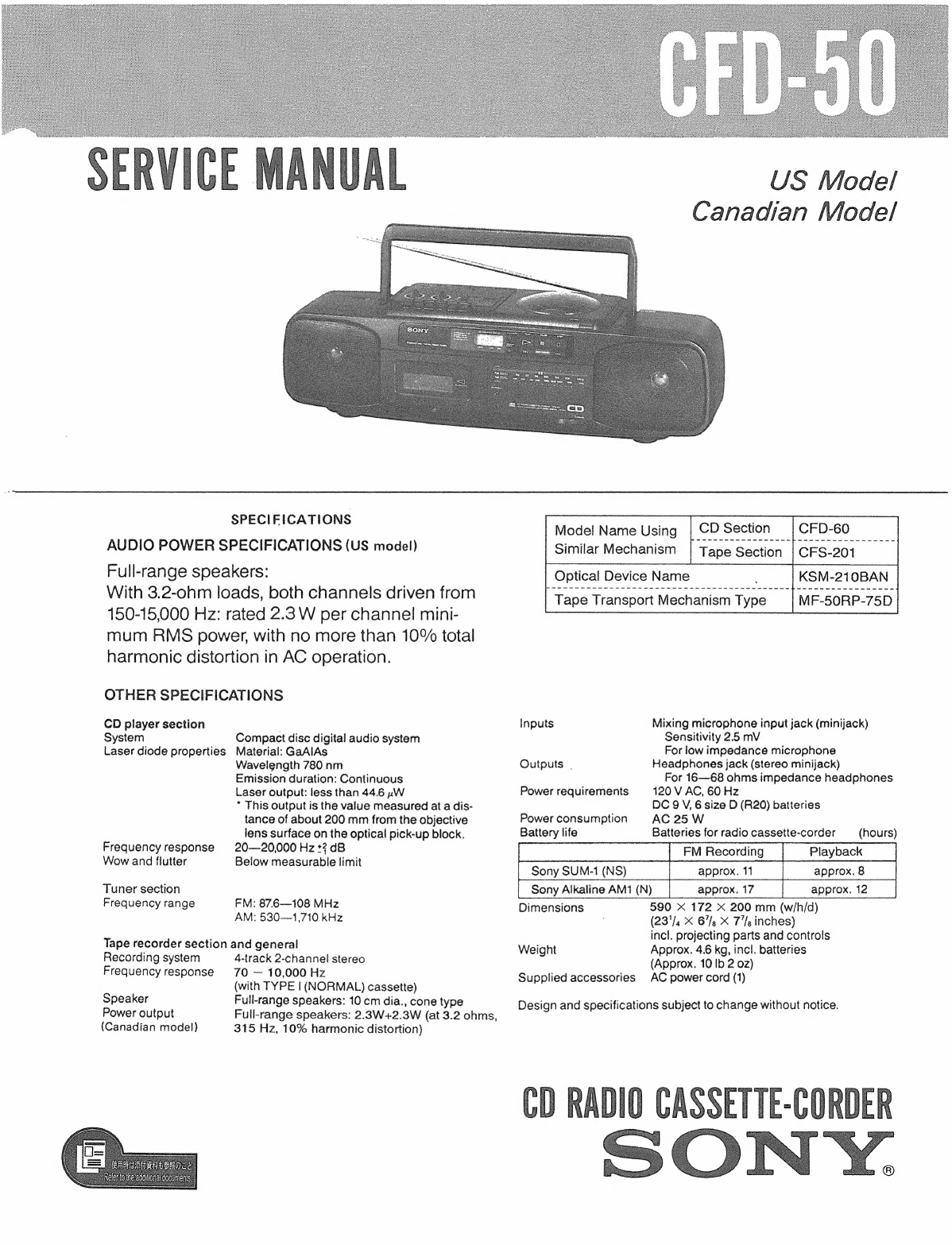
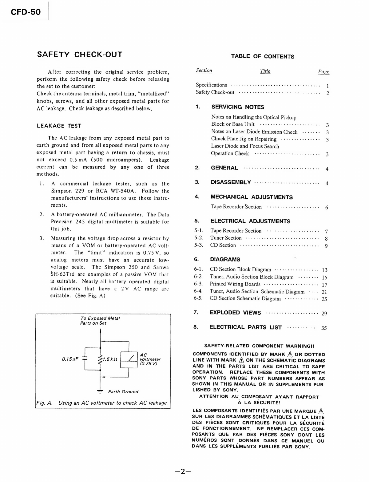
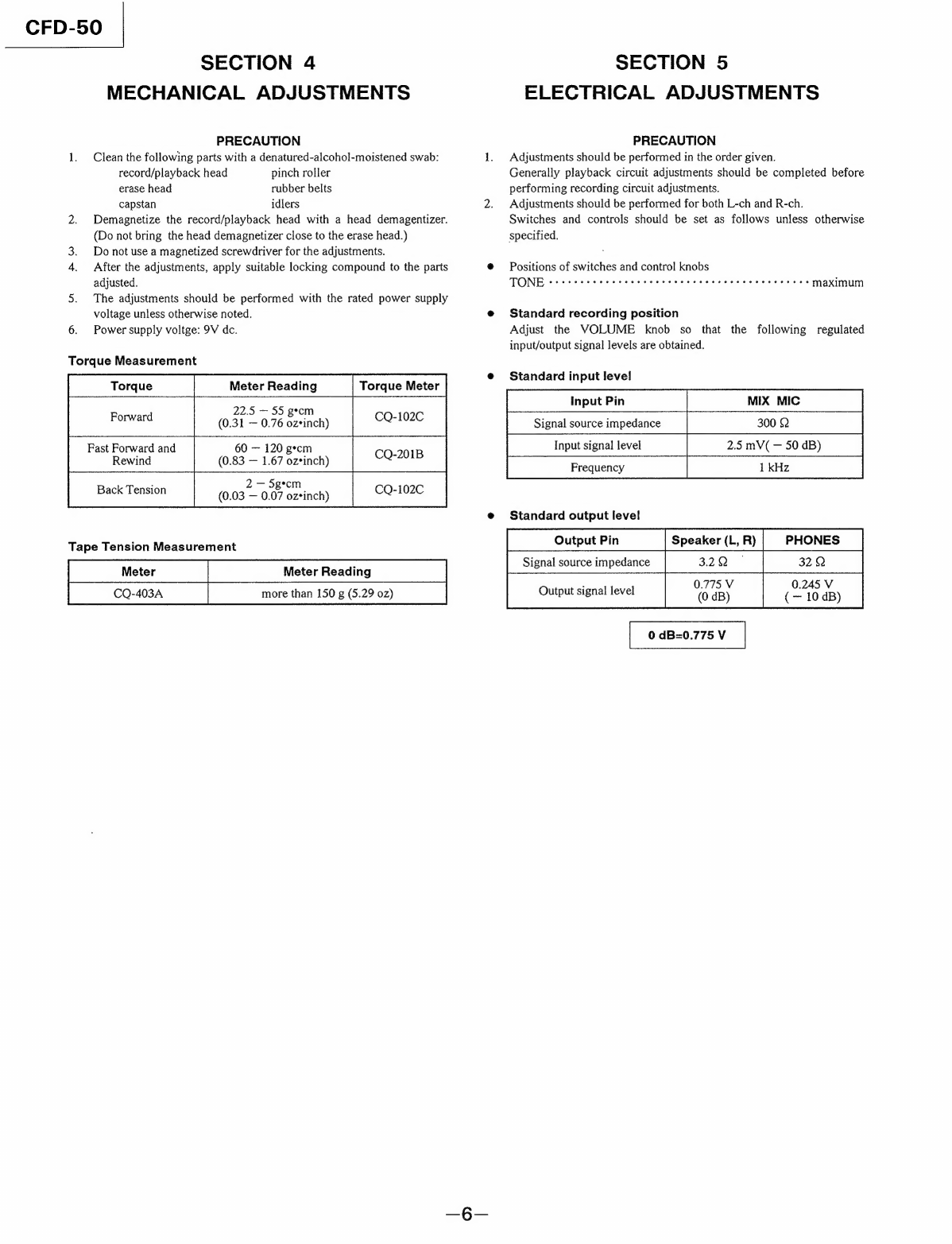
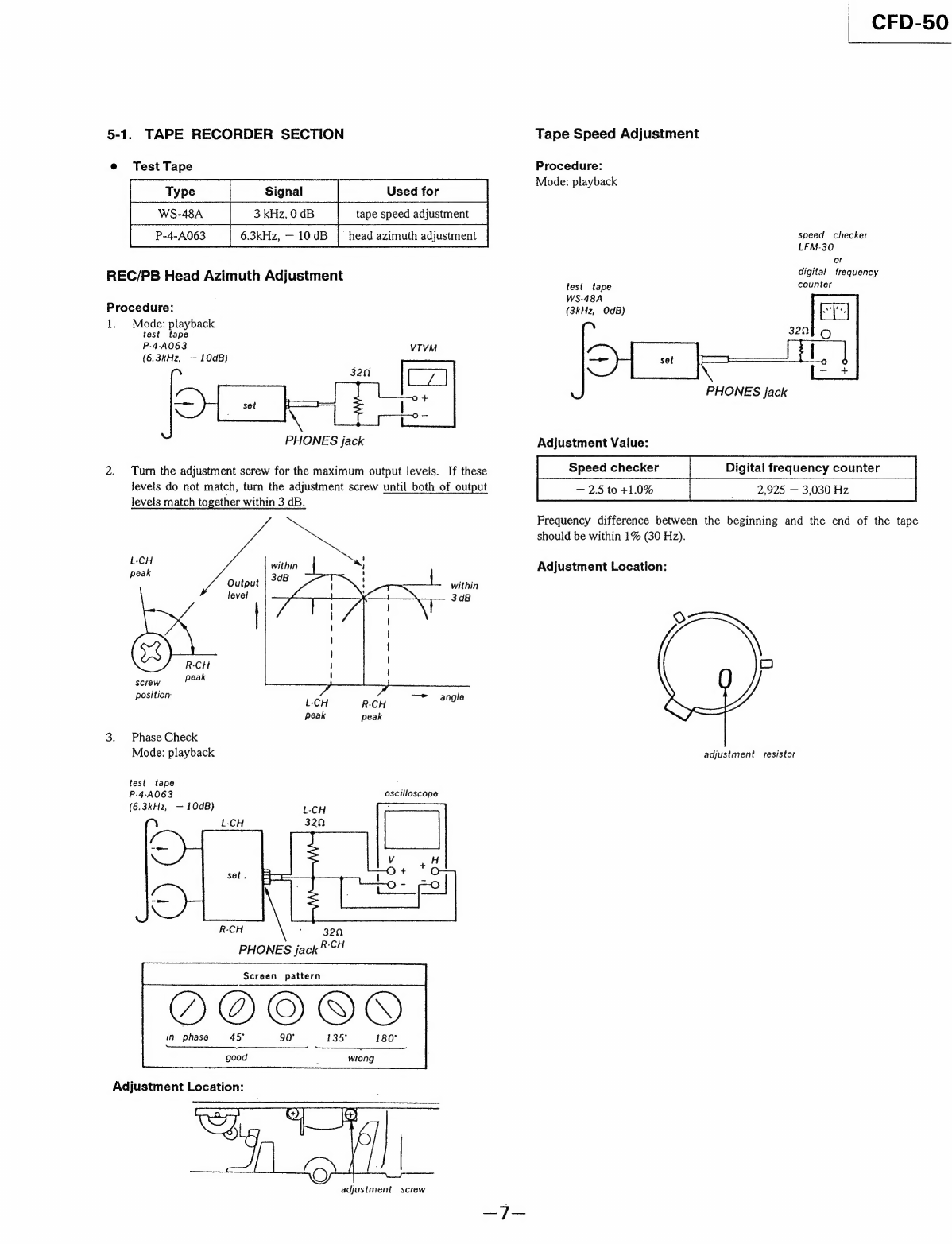
Sony CFD-50 User manual

US
Model
Canadian
Model
SPECIFICATIONS
AUDIO
POWER
SPECIFICATIONS
(US
model)
Full-range
speakers:
With
3.2-ohm
loads,
both
channels
driven
from
150-15,000
Hz:
rated
2.3
W
per
channel
mini-
mum
RMS
power,
with
no
more
than
10%
total
harmonic
distortion
in
AC
operation.
OTHER
SPECIFICATIONS
CD
player
section
System
Laser diode
properties
Compact
disc
digital
audio
system
Material:
GaAlAs
Wavelength
780
nm
Emission
duration:
Continuous
Laser
output:
less
than
44.6
p.W
*
This
output
is
the
value
measured
at
a
dis-
tance
of
about
200
mm
from
the
objective
lens
surface
on
the
optical
pick-up
block.
20-—20,000
Hz
+?
dB
Below
measurable
limit
Frequency
response
Wow
and
flutter
Tuner
section
Frequency
range
FM:
87.6—108
MHz
AM:
530—1,710
kHz
Tape
recorder
section
and
general
Recording
system
4-track
2-channel
stereo
Frequency
response
70
—
10,000
Hz
(with
TYPE
|
(NORMAL)
cassette)
Full-range
speakers:
10
cm
dia.,
cone
type
Full-range
speakers:
2.3W+2.3W
(at
3.2
ohms,
315
Hz,
10%
harmonic
distortion)
Speaker
Power
output
(Canadian
mode!)
CD
Section
Tape
Section
Model
Name
Using
Similar
Mechanism
Optical
Device
Name
MF-50RP-75D
Tape
Transport
Mechanism
Type
Inputs
Mixing
microphone
input
jack
(minijack)
Sensitivity
2.5
mV
For
low
impedance
microphone
Outputs
Headphones
jack
(stereo
minijack)
For
16—68
ohms
impedance
headphones
120
V
AC,
60
Hz
DC
9
V,
6
size
D
(R20)
batteries
AC
25
W
Power
requirements
Power
consumption
Battery
life
Batteries
for
radio
cassette-corder
(hours)
[_SS*d;CF
Recording
[Playback
Sony
SUM-1
(NS)
Sony
Alkaline
AM1
(N)
approx.
8
approx.
12
approx.
17
Dimensions
590
X
172
X
200
mm
(w/h/d)
(23/4
X
67/,
X
7/3
inches)
incl.
projecting
parts
and
controls
Weight
Approx.
4.6
kg,
incl.
batteries
(Approx.
10
Ib
2
oz)
Supplied
accessories
AC
power
cord
(1)
Design
and
specifications
subject
to
change
without
notice.
CD
RADI

CFD-50
SAFETY
CHECK-OUT
After
correcting
the
original
service
problem,
perform
the
following
safety
check
before
releasing
the
set
to
the
customer:
Check
the
antenna
terminals,
metal
trim,
‘‘metallized”’
knobs,
screws,
and
all
other
exposed
metal
parts
for
AC
leakage.
Check
leakage
as
described
below.
LEAKAGE
TEST
The
AC
leakage
from
any
exposed
metal
part
to
earth
ground
and
from
all
exposed
metal
parts
to
any
exposed
metal
part
having
a
return
to
chassis,
must
not
exceed
0.5mA
(500
microampers).
Leakage
current
can
be
measured
by
any
one
of
three
methods.
1.
A
commercial
leakage
tester,
such
as
the
Simpson
229
or
RCA
WT-540A.
Follow
the
manufacturers’
instructions
to
use
these
instru-
ments.
2.
A
battery-operated
AC
milliammeter.
The
Data
Precision
245
digital
multimeter
is
suitable
for
this
job.
3.
Measuring
the
voltage
drop
across
a
resistor
by
means
of
a
VOM
or
battery-operated
AC
volt-
meter.
The
“limit”
indication
is
0.75
V,
so
analog
meters
must
have
an
accurate
low-
voltage
scale.
The
Simpson
250
and
Sanwa
SH-63Trd
are
examples
of
a
passive
VOM
that
is
suitable.
Nearly
all
battery
operated
digital
multimeters
that
have
a
2V
AC
range
are
suitable.
(See
Fig.
A)
To
Exposed
Metal
Parts
on
Set
AC
voltmeter
(0.75
V)
Earth
Ground
Using
an
AC
voltmeter
to
check
AC
leakage.
TABLE
OF
CONTENTS
Section
Title
Page
Specifications
sass
sors
Hepes
aciued
dea
ee
csoees
1
Safety
Check-out
#098
Op
Sie!
aig
6S
SS
ees
oe
br
aitele,
858.08
02.6,
8
2
1.
SERVICING
NOTES
Notes
on
Handling
the
Optical
Pickup
Block
or
Base
Unit
a
3
Notes
on
Laser
Diode
Emission
Check
-----+-
3
Chuck
Plate
Jig
on
Repairing
--+++++++++eee-
a
Laser
Diode
and
Focus
Search
Operation
Check
a
3
2.
GENERAL.
«222%
+sisse
cbse
smesysee
dunes
4
3.
DISASSEMBLY
..----.-----eecceeecceees
4
4.
MECHANICAL
ADJUSTMENTS
Tape
Recorder
Section
-++++eeeeeeeeeeeeeee
6
5.
ELECTRICAL
ADJUSTMENTS
5-1.
Tape
Recorder
Section
--+++++err
essere
sees
7
5-2.
Tuner
Section
Ostia
pa,
Bie:
ele
cone!
Bete.
e-e
8
eee
ow
wie
eos
Ss
8
5-3.
CD
Section
wi
Oe:
S18)
0060
0:
Sah
ec
Oe
eee
6
6:
eee
wae
9
6.
DIAGRAMS
6-1.
CD
Section
Block
Diagram
-+++++++++++-+-+--
13
6-2.
Tuner,
Audio
Section
Block
Diagram
-+---++:-
1S
6-3.
Printed
Wiring
Boards
---+++-++++eee
eee
eeee
17
6-4.
Tuner,
Audio
Section
Schematic
Diagram
2)
6-S.
CD
Section
Schematic
Diagram
-++++++++++-
25
7.
EXPLODED
VIEWS
.«.---------eseeeeeee
29
8.
ELECTRICAL
PARTS
LIST
.-----------
35
SAFETY-RELATED
COMPONENT
WARNING!!
COMPONENTS
IDENTIFIED
BY
MARK
A\
OR
DOTTED
LINE
WITH
MARK
/\
ON
THE
SCHEMATIC
DIAGRAMS
AND
IN
THE
PARTS
LIST
ARE
CRITICAL
TO
SAFE
OPERATION.
REPLACE
THESE
COMPONENTS
WITH
SONY
PARTS
WHOSE
PART
NUMBERS
APPEAR
AS
SHOWN
IN
THIS
MANUAL
OR
IN
SUPPLEMENTS
PUB.
LISHED
BY
SONY.
ATTENTION
AU
COMPOSANT
AYANT
RAPPORT
A
LA
SECURITE!
LES
COMPOSANTS
IDENTIFIES
PAR
UNE
MARQUE
/\
SUR
LES
DIAGRAMMES
SCHEMATIQUES
ET
LA
LISTE
DES
PIECES
SONT
CRITIQUES
POUR
LA
SECURITE
DE
FONCTIONNEMENT.
NE
REMPLACER
CES
COM.
POSANTS
QUE
PAR
DES
PIECES
SONY DONT
LES
NUMEROS
SONT
DONNES
DANS
CE
MANUEL
OU
DANS
LES
SUPPLEMENTS
PUBLIES
PAR
SONY.

SECTION
1
CFD-50
SERVICING
NOTES
NOTES
ON
HANDLING
THE
OPTICAL
PICK-
UP
BLOCK
OR
BASE
UNIT
The
laser
diode
in
the
optical
pick-up
block
may
suffer
electrostatic
breakdown
because
of
the
poten-
tial
difference
generated
by
the
charged
electrostatic
load,
etc.
on
clothing
and
the
human
body.
During
repair,
pay
attention
to
electrostatic
break-
down
and
also
use
the
procedure
in
the
printed
matter
which
is
included
in
the
repair
parts.
The
flexible
board
is
easily
damaged
and
should
be
handled
with
care.
NOTES
ON
LASER
DIODE
EMISSION
CHECK
The
laser
beam
on
this
model
is
concentrated
so
as
to
be
focused
on
the
disc
reflective
surface
by
the
objective
lens
in
the
optical
pick-up
block.
There-
fore,
when
checking
the
laser
diode
emission,
observe
more
than
25
cm
away
from
the
objective
lens.
Insert
screwdriver
and
push
S801.
CHUCK
PLATE
JIG
ON
REPAIRING
On
repairing
CD
section,
playing
a
disc
without
the
CD
lid,
use
Chuck
Plate
Jig.
@
Code
number
of
Chuck
Plate
Jig:
X-4918-255-1
LASER
DIODE
AND
FOCUS
SEARCH
OPERATION
CHECK
1,
Der
eae
t
Ae
|
ae
ai
Make
Function
switch
to
CD
position
with
no
disc
inserted.
Open
the
lid
for
CD.
Turn
on
S801
as
following
figure.
Press
®
key.
Confirm
the
laser
diode
emission
while
observing
the
objecting
lens.
When
there
is
no
emission,
Auto
Power
Control
circuit
or
Optical
Pick-up
is
broken.
Objective
lens
moves
up
and
down
once
for
the
focus
serarch.
Yf.
~~
|
AS
S801
AL
27.
eee
yvilty,
pe
a
laser
diode

CFD-50
SECTION
2
GENERAL
e
Parts
Identification
Radio,
Tape
Section
.
CD
Player
Section
MIX
MIC
jack
OPRI/BATT
indicator
Telescopic
antenna
FUNCTION
selector
Display
window
PLAY
MODE
button
Disc
holder
TONE
control
OPEN
button
VOLUME
cont
PHONES
jack
CD
operation
buttons
Cassette
holder
Tape
operation
buttons
-
ae
REMAIN/ENTER
button
indicator
SECTION
3
DISASSEMBLY
Note:
Follow
the
disassembly
procedure
in
the
numerical
order
given.
DIAL
POINTER
SETTING
@
Set
the
center
of
the
dial
pointer
to
the
center
of
three
points
on
the
sub
chassis.
@
til
gs
pointer
to
the
dial
pointer
sub
chassis
dial
pointer
©
Turn
PVC
gear
fully
counter-clockwise
with
the
tuning
knob.
tuner
board
@
Insert
the
tuning
knob
@
Turn
the
tuning
knob
in
the
order
of
frequency
MAX
~->
MIN
and
confirm
the
dial
pointer
is
not
out
of
order.
s
@
+BVIP3
X
12

CFD-50
FRONT
CABINET
@
Open
cassette
holder.
@
CNJ302
@
front
cabinet
©
BVTP3
x
40
©
BVTP3
x
40
j
@
battery
case
lid
@
+BVTP3
X
12
TUNER
BOARD
@
+BVTP3
x
12
@
tuner
board
es,
MD
SECTION
©
CNJ21
@
CNJ306
CD
MAIN
BOARD
AUDIO
BOARD
OSB
Trs
rik
©
CD
main
board
@
Remove
two
volume
knobs.
@
Slide
out
CD
section
(VOLUME,
TONE)
©
+BVTP3
X
129
i
§
©
+BVTP3
X
12
®
audio
board
POWER
BOARD
@
+BVTP3
X
12
@
power
board

CFD-50
SECTION
4
MECHANICAL
ADJUSTMENTS
PRECAUTION
1.
Clean
the
following
parts
with
a
denatured-alcohol-moistened
swab:
record/playback
head
pinch
roller
erase
head
rubber
belts
capstan
idlers
2.
Demagnetize
the
record/playback
head
with
a
head
demagentizer.
(Do
not
bring
the
head
demagnetizer
close
to
the
erase
head.)
3.
Do
not
use
a
magnetized
screwdriver
for
the
adjustments.
4.
After
the
adjustments,
apply
suitable
locking
compound
to
the
parts
adjusted.
5.
The
adjustments
should
be
performed
with
the
rated
power
supply
voltage
unless
otherwise
noted.
6.
Power
supply
voltge:
9V
dc.
Torque
Measurement
22.5
—
55
gecm
Fast
Forward
and
60
—
120
g*cm
(0.83
1.67
ozrinchy
|
COMI
:
2
—
Sgecm
(0.03
=
0.07
ozrinchy
|
|
SO
Tape
Tension
Measurement
CQ-403A
more
than
150
g
(5.29
02)
SECTION
5
ELECTRICAL
ADJUSTMENTS
PRECAUTION
Adjustments
should
be
performed
in
the
order
given.
Generally
playback
circuit
adjustments
should
be
completed
before
performing
recording
circuit
adjustments.
Adjustments
should
be
performed
for
both
L-ch
and
R-ch.
Switches
and
controls
should
be
set
as
follows
unless
otherwise
specified.
Positions
of
switches
and
control
knobs
TONE
BO
OOO
ROHS
ie:
CLO
OO
6
06
0168.
O08
6.656
SOE
8)
OS
8
ON
Oe
0180
O88
are)
maximum
Standard
recording
position
Adjust
the
VOLUME
knob
so
that
the
following
regulated
input/output
signal
levels
are
obtained.
Standard
input
level
[—__tput
ind
Standard
output
level
[Output
Pin
[Speaker
A)]
PHONES
Output
signal
level
“0
cB
)
Wee
ie
0
dB=0.775
V

5-1.
TAPE
RECORDER
SECTION
@
Test
Tape
|
Type
|
Signal
=|
Used
for
WS-48A
3
kHz,
0
dB
tape
speed
adjustment
P-4-A063
6.3kHz,
—
10
dB
|
head
azimuth
adjustment
REC/PB
Head
Azimuth
Adjustment
Procedure:
1.
Mode:
playback
test
tape
P-4-A063
(6.3kHz,
—
10dB)
PHONES
jack
2.
Turn
the
adjustment
screw
for the
maximum
output
levels.
If
these
levels
do
not
match,
turn
the
adjustment
screw
until
both
of
output
levels
match
together
within
3
dB.
L-CH
|
~
peak
within
Output
Zan
i
within
level
3d8
!
}
!
I
|
R-CH
screw
peak
aie
osition
positi
L-CH
R-CH
—*
angle
peak
peak
3.
Phase
Check
Mode:
playback
test
tape
P.4-A063
oscilloscope
(6.3kHiz,
:
—
10d8)
320
PHONES
jack
®C4
Screen
pattern
O@®
QO
135°
180°
es
wrong
in
phase
45° 90°
oceennmennteenmmeenen
ammamenmemeeemenamnenendtl
good
Adjustment
Location:
adjustment
screw
|
CFD-50
Tape
Speed
Adjustment
Procedure:
Mode:
playback
speed
checker
LFM-30
or
digital
frequency
test
tape
counter
WS-48A
(3kHz,
OdB)
PHONES
jack
Adjustment
Value:
Speed
checker
Digital
frequency
counter
—
2.5
to
+1.0%
2,925
—
3,030
Hz
Frequency
difference
between
the
beginning
and
the
end
of
the
tape
should
be
within
1%
(30
Hz).
Adjustment
Location:
O
adjustment
resistor

CFD-50
|
5-2.
TUNER
SECTION
[AM]
FUNCTION
switch:
AM
AM
RF
SSG
Put
the
lead-wire
antenna
close
to
we
the
set.
(QE
aE
30%
amplitude
modulation
by
400
Hz
signal
output
level:
as
low
as
possible
[FM]
FUNCTION
switch:
FM
FM
RF
SSG
22.5
kHz
frequency
deviation
‘by
400
Hz
signal
output
level:
as
low
as
possible
to
FM
ANT
IN
PHONES
@
Repeat
the
procedures
in
each
adjustment
several
times,
and
the
frequency
coverage
and
tracking
adjustments
should
be
finally
done
by
the
trimmer
capacitors.
AM
IF
ADJUSTMENT
Adjust
for
a
maximum
reading
on
VITVM.
455
kHz
AM
FREQUENCY
COVERAGE
ADJUSTMENT
Adjust
for
a
maximum
reading
on
VT
VM.
520
kHz
1,780
kHz
AM
TRACKING
ADJUSTMENT
Adjust
for
a
maximum
reading
on
VTVM.
600
kHz
1,500
kHz
FM
TRACKING
ADJUSTMENT
Adjust
for
a
maximum
reading
on
VTVM.
.
86.5
MHz
109.5
MHz
FM
VCO
Adjustment
A)
Regular
Method
Procedure:
FM
ff
signal
generator
=
po
Carrier
frequency
:
98MHz
telescopic
Modulation:
no
modulation
antenna
lead
Output
level:
0.1V
(100dB)
Remove
jumper
wire
as
shown
below.
Connect
frequency
counter
to
the
positions
shown
below.
Tune
the
set
to
98
MHz.
Adjust
RV1
for
76
kHz
+
500
Hz
reading
on
the
frequency
counter.
After
adjustment,
connect
jumper
wire
removed
in
step
1.
Remove
jumper
wire
Aaa
Noe
frequency
counter
nee)
Bere
B)
Simple
Method
Procedure:
1.
Tune
the
set
to
the
FM
stereo
broadcasting
signal.
2.
Turn
RV1
clockwise
or
counterclockwise
and
memorize
the
lighting-
up
range
of
the
FM
STEREO
lamp.
3.
Secure
RVI
at
the
center
of
the
lighting-up
range
of
both
turns
as
shown
below.
center
of
lighting-up
ranges
lighting-up
range
iO)
/
,
N
N
ee
Sao
RVI
FM
FREQUENCY
EMVvco
COVERAGE
RV1
L2
cCT2
AM
TRACKING
11
CTi
Li
CT4
L4
AMIE
CEM
FREQUENCY
—38—
TRACKING
GovERAGE

5-3.
CD
SECTION
How
to
Put
the
Set
into
Service
Mode
Notes
on
Adjustment
1.
Perform
adjustment
in
service
mode.
After
adjustment,
be
sure
to
release
service
mode.
2.
Perform
adjustments
in
the
order
given.
3.
Use
the
disc
(YEDS-18,
Part
No.
3-702-101-01)
only
when
so
indicated.
1.
Short-circuit
following
portions
on
the
CD
main
board.
2.
Tune
the
POWER
on.
CD
main
board
(conductor
side)
:
short-circuit
Before
Adjustment
Put
the
set
into
service
mode
and
perform
the
following
checks.
Repair
if
there
are
any
problems.
Le
eS
[ee
|
e
Sled
Motor
Check
1.
Press
®
key,
then
press
I
key.
Press
PPI,
Kd
keys
and
confirm
that
the
FOP
moves
smoothly
from
the
innermost
to
outermost
circumference
and
back
smoothly
and
with
no
catching
or
abnormal
noises.
pb]
:
FOP
moves
to
the
outer
circumference
K4q
:
FOP
moves
to
the
inner
circumference
@
Focus
Search
Check
Press
>
key.
(Focus
search
operation
is
performed
continuously.)
Look
at
the
FOP
objective
lens
and
confirm
that
it
moves
up
and
down
smoothly,
with
no
catching
or
abnormal
noises.
3.
Press
Ml
key.
Confirm
that
focus
search
operation
stops.
If
it
does
not,
press
Il
key
again
longer.
N=
VCO
Adjustment
Adjustment
Procedure:
1..
Short-circuit
@
portion
CD
main
board.
2.
Adjust
with
RV703
so
that
the
reading
on
frequency
counter
becomes
4.3218
MHz.
3.
Release
the
short-circuit
@
portion.
Adjustment
Location:
CD
main
board
(conductor
side)
frequency
counter

E-F
Balance
Adjustment
This
adjustment
is
to
be
done
when
the
optical
block
is
replaced.
Adjustment
Procedure:
:
Connect
the
oscilloscope
between
IC701
pins
@
and
@.
Put
the
set
into
service
mode.
(See
page
9)
Press
the
PP]
and
k4q
keys
to
move
the
FOP
to
the
center.
Insert
disc
(YEDS-18)
and
press
}
key.
Adjust
RV701
so
that
the
oscilloscope
traverse
waveform
is
symmetrical,
as
shown
in
the
figure
below.
Release
service
mode
after
adjustment
is
completed.
A
8
VOLT/DIV:
1V
TIME/OIV:
Ims
Adjustment
Location:
CD
main
board
(conductor
side)
RV702
RV701
Focus
Bias
Adjustment
This
adjustment
is
to
be
done
when
the
optical
block
is
replaced.
Adjustment
Procedure:
Connect
the
oscilloscope
between
IC701
pins
@
and
@.
Put
the
set
into
service
mode.
(See
page
9)
__
Press
the
PP]
and
K¢q
keys
to
move
the
FOP
to
the
center.
(Move
the
FOP
to
the
music
area
on
the
disc
to
enable
easy
visibility
of
the
eye
pattern.)
Insert
disc
(YEDS-18)
and
press
>
key.
Adjust
RV702
so
that
the
oscilloscope
waveform
is
as
shown
in
the
figure
below(eye
pattern).
A
good
eye
pattern
means
that
the
diamond
shape
(©
)
in
the
center
of
the
waveform
can
be
clearly
distinguished.
Release
service
mode
after
adjustment
is
completed.
RF
signal
reference
waveform
(eye
pattern)
\RXANA
i
Wie
i
\\
VOLT/OIV
:
0.2V
TIME/OIV
:
500ns
0.8
—
1.5
Vp-p
Hii
MA
Way
Wy
ov
When
observing
the
eye
patern,
set
the
oscilloscope
for
AC
range
and
raise
vertical
sensitivity.
E-F
Balance
Adjustment
oscilloscope
(DC
range)
ES
Focus
Bias
Adjustment
+
oscilloscope
(DC
range)

REFERENCE
Focus/Tracking
Gain
Adjustment
A
frequency
response
analyzer
is
necessary
in
order
to
perform
this
adjustment
exactly.
However,
this
gain
has
a
margin,
so
even
if
it
is
slightly
off,
there
is
no
problem.
Therefore,
do
not
perform
this
adjustment.
Focus/tracking
gain
determines
the
pick-up
follow-
up
(vertical
and
horizontal)
relative
to
mechanical
noise
and
mechanical
shock
when
the
2-axis
device
operate,
However,
as
these
reciprocate,
the
adjustment
is
at
the
point
where
both
are
satisfied.
@
When
gain
is
raised,
the
noise
when
the
2-axis
device
operates
increases.
@
When
gain
is
lowered,
it
is
more
susceptible
to
mechanical
shock
and
skipping
occurs
more
easily.
@
When
gain
adjustment
is
off,
the
symptoms
below
appear.
low
or
high
@
The
time
until
music
starts
becomes
longer
for
STOP
=P
PLAY
or
automatic
selection
(Hed
PR
buttons
pressed.
(Normally
takes
about
2
seconds.)
e
Music
does
not
start
and
disc
continues
to
rotate
for
STOP
=>
PLAY
or
automatic
selection
(Hed
bi
buttons
pressed.)
e
Sound
is
interrupted
dur-
ing
PLAY.
Or
time
count-
er
display
stops
progress-
ing.
e
More
poise
during
2-axis
device
operation.
The
following
is
a
simple
adjustment
method.
—
Simple
Adjustment
—
Note:
Since
exact
adjustment
cannot
be
performed,
remem-
ber
the
positions
of
the
controls
before
performing
the
adjustment.
If
the
positions
after
the
simple
adjust-
ment
are
only
a
little
different,
return
the
controls
to
the
original
position.
Procedure:
1.
Keep
the
set
horizontal.
If
the
set
is
not
horizontal,
this
adjustment
cannot
be
performed
due
to
the
gravity
against
the
2
axis
device.
2.
Insert
disc
(YEDS-18)
and
press
®»
PLAY
button.
3.
Connect
the
oscilloscope
between
IC701
pins
62)
and
6)
.
4.
Adjustment
RV705
so
that
the
waveform
is
as
shown
in
the
figure
below.
(focus
gain
adjustment)
@
Incorrent
Examples
(DC
level
changes
more
than
on
adjusted
waveform)
low
focus
gain
—-OV
VOLT/DIV:
TIME/DIV:
2mS
VOLT/DIV:
TIME/DIV:
2mS
—
250mvVv
700
mV
100
mV
VOLT/DIV:
100
mv
TIME/DIV:
2mS
5.
Connect
the
oscilloscope
between
IC701
pins
@)
and
26)
:
6.
Adjust
RV704
so
that
the
waveform
is
as
shown
in
the
figure
below.
(tracking
gain
adjustment)
VOLT/DIV:
1V
TIME/DIV:
2ms
OV
@
Incorrect
Examples
(fundamental
wave
appears)
low
tracking
gain
VOLT/DIV:
1V
TIME/DIV:
2mS
—
OV
high
tracking
gain
(higher
fundamental
wave
than
for
low
gain)
VOLT/DIV:
1V
TIME/DIV:
2mS
—
Ov
Adjustment
Location:
CD
main
board
(conductor
side)
Remove
the
solder
bridge
while
-
adjusting
the
tracking
gain.
(After
adjustment
make
the
solder
bridge.)
oscilloscope
(DC
range)
Remove
the
solder
bridge
while
adjusting
the
focus
gain.
——
(After
adjustment
make
the
solder
bridge.)
RV705
1C701
pin
@
1C701
pin
@
IC701
pin
@
RV704

SECTION
6
DIAGRAMS
6-1.
CD
SECTION
BLOCK
DIAGRAM
XF701
C2F2
OPTICAL PICK-UP
O
Seess
aa
BLOCK
{C707
1c706
cco
5
CHES)
D/A
CONVERTER
LPF
i
wu
No
oOo
i
|
TO
@
RADIO
BLOCK
v
r
Q
x
x
r
1c703
CO
OIGITAL
SIGNAL
PROCESSOR
Lt
u
|
y
AUDIO
MUTE
DE~EMPHASIS
:
.
Q702.
712
Q703.
713
O
:
Le
ee
ee
|
I
|
|
i
i
|
{
I
I
|
l
|
I
|
I
RV7O4
ar
AUDIO
MUTE
DRIVE
PEN
EMPHASIS
DRIVE
BALANCE
Q@704,
705
Q741.
714
DAOS
-
DADA
(
28-32,
34-37)
34-37
LASER POWER
CONTROL
LD
O
@
—
O
a
x
~
$601
OPEN/CLOSE
O
©
ssogs
REMAIN/
nara
BEr
-
Re
nee
al
PLAY
MODE
oO
+
O
aig
a
es
ee
ee
colt
'.
Se
eae
eee
eae
i
ee
{c708
1c802
FOCUS,
TRACKING
COIL
FILTER
ORIVE
|
88
FS
9
9
z
ees
oe
i
aie
poet
pa
cS
tcso1
O-
SYSTEM
CONTROL
1+(6)
sabe
@
(6)
MUTE
$806
1c708
paras
Sane
3.
10702
SLED.
SPINDLE
MOTOR
CD
SYSTEM
DRIVE
SERVO
PROCESSOR
Ane
of
SYSTEM
RESET
@
ore
©
SWITCH
pa
ae
to
ae
REC
ee
(18)
REC
REG
+
+
CO
+8
e706
SV
()
M702
SPINDLE
O
v
S802
©
LIMIT
FROM
RADIO
BLOCK
G0)
P
CON
LCD1
eal
FS
ae
—14—

6-2.
TUNER,
AUDIO
SECTION
BLOCK
DIAGRAM
ANT!
FM
TELESCOPIC
ANTENNA
\
FL14
FM/AM
FRONT-END.
IF,
DEMODE
Rv1
G)vco
FM
VCO
L
FROM
A
CD
BLOCK
R
J301
|
MIX
MIC
$302
RECORD/PLAYBACK
PLAYBACK
=
RECORD
HRP601
RECORD/PLAYBACK
HEAD
HEGO1
ERASE
X
HEAD
SEL
DET
LPF
SP802
R
$301
[FUNCTION
|
TAPE
—
AM
—+
FM
—
CD
L
DRIVE
Q102
(ste
REO
—15—
MIC
AMP
Q301,
302
$302-1
nee
|
$301-1
$601
[FUNCTION
]
MOTOR
TAPE
>
AM
>
FM
>
CD
REC
SWITCH
Q307
J302
PHONES
MUTING
Q101
1c302
POWER
AMP
lavso1-2
ee
vai
0901-904
RECT
+B+5V
Vcc
+9V
~t—
BIAS
CONTROL
SWITCHING
SWITCH
Q308
Q304,
0304
oe
ee,
:
DRY
BATTERY
'
M601
0307
+
SIZe
“p"
REEL/Y
6PCS,
9V
epee
(OPR/BATT)
a
=
Q306
me
CD
BLOCK
REC
i
—1
6—

|
23
20
19
19
14
‘11
10
PRINTED
WIRING
BOARDS
6-3.
24.
|
5
TELESCOPIC
ANTENNA
{TUNER
BOARD
}
UP
BLOCK
-210B)
OPTICAL
PICK-
(KSS
ae
SRE,
[CD
CONTROL
BOARD]
(COMPONENT
SIDE)
D
MAIN
BOARD
[‘
ROD
ANTENNA
FERRITE
wr
Se
<
SRR
RNARRRRSE
RODE
RRR
eR
Ou
See
ERR
RR
AREER
RIE
CNJ2I
6PCS
9V
{EC
DESIGNATION
R20
“7
DRY
BATTERY
SIZE
"D"
*
{POWER
BOARD]
CNJ
702
(AUDIO
BOARD)
x“
rs)
4
o
_>
3s
Of
on
fa
De
3
oS
w
a
HEAD
{CD
MOTOR
BOARD]
a
Se
SENN
YIP
SEIS
SE
SETH
:
HIT
LRN
—
eT!
2
Sbancremmeenno
—
CNJ
713
gunn
ng
ROR
ONSET
TA
HN
SE
ARETE
TEES
SET
SS
NENT
TSN
RNY
SHES
STATA
NSE
ST
ETT
SERENE
STN
eaters
BLK
{MD
BOARD]
ee
ee
a,
ae
pTLA
TTS
pS
SATS
NE
ET
PI
SST
NEESER
ATEN
SSE
SSNS
gE
SSN
NEN
NN
TT
NE
ANE
SEE
[CD
LEAF
SW
BOARD]
Parts
extracted
from
the
component
side
f
2
rer]
is0]
9g
°
pa
2]
<
oO
=
O|z2
s
+
©
G
ca
ole
7]
Le]
&
ai
~—_
=
he
=
Sis
32
Sik
¢
°
i
ae)
‘Soe
<
-
a
°
S
Lis
®
~
oO;
=
{e)
Y}2
Z2e
a
e
SSR
Pp
REA
TRATES
3
Se
S
pS
ESI
npn
RESORT
CNJ
705
M60
REEL
/CAPSTAN
(R-CH)
SPEAKER
SPEAKER
(L~CH)
3302
PHONES
D307
OPR/BATT
—138—
e
Circuit
Boards
Location
CD
leaf
switch
board
power
board
CD
motor
board
OPTICAL
PICK
UP
board
CD
main
board
audio
board
MD
board
tuner
board
—20—

6-4.
TUNER,
AUDIO
SECTION
SCHEMATIC
DIAGRAM
1
2
3
4
5
6
7
8
9
10
11
12
13
14
15
16
17
18
19
20
21
22 23 24
25
26
e
ic
i
.
Block
Diagram
1C1
CXA1238S
ANT!
B
nega
=
-
_
-
+
-
—_
-
—_
-
__
-—__-
!
(TUNER
BOARD]
|
Paarroweo
;
hy
AY
—
3 =
2
“
<5,
to
een
FM
IF/
°
=
2
a
vco
’
ISCRI.
3
s
a
_
aii
Cc
“
“
>
8
SLR-34VR
-
5
8
8
FM
STEREO
I
FM/AM
FRONT-END,
o
°
[
FM
STEREO
|
ry
coun
eR
oO
<|
pe
-OEMODE
st
TCU
1/2
COUNTER
(°02)
TUNING
La
INDIC
ATOR
BAND
PASS
MUTE
FE
QUT
NO
RF
IN
FM
RF
AFC
;
AM
OSCMUTE
FM
®ISCRI
MPX
REG
GNB
ee
1.25V
vco
PLL LPF
D
1
BAND
IF,
DET
U
VGQ
CHECK
_LP
|
|
SELECT
AM
IF
IN
FM
IF
IN
TUNING
GND
AGC:
AFC
St
oN
P
tor
DET
PLL LPF
]
|
Note
on
Schematic
Diagram:
e@
All
capacitors
are
in
uF
unless
otherwise
noted.
pF:
MMF
7
SOWV
or
fess
are
not
indicated
except
for
electrolytics
and
tantalums.
®
All
resistors
are
in
2
and
'/,W
or
less
unless
otherwise
specified.
I
e
fF
:
fusible
resistor.
©
F
I
:
adjustment
for
repair.
Voltage
and
waveforms
are
dc
with
respect
te
ground
FE
under
nosignal
(detuned)
conditions.
Radio
section
no
mark:
FM
Ooo
Tr
Ce
I
OF
[AUDIO
BOARD]
KH301
,9]
®
te
Tape
section.
<a
no
mark:
PLAY
‘
it)
ee
ee
(
):
REC
G
s&
Q301,
302
FUNCTION
CD
section
eA
MIC
AMP
FM:
a
no
mark:
STOP
Q30!
(
):
PLAY
25C1740S-S
5
pterses
@
Voltages
are
taken
with
a
VOM
(10
MQ/V).
.
4
SWITCHING
Voltage
variations
may
be
noted
due
to
normal
produc-
i
Lo
4
=
=
ee
>
>
>
-
(LAM
R222
12k
R122
12k
anS+
3.
]
tion
tolerances,
uo.
CNP30S
e
Waveforms
are
taken
with
a
oscilloscope.
L304
¢
baw
Lo
GHA
Se
|
i
R331
4.7k
R123
2,
2k
|
Ri27
15k
Ri25
12k
a
mo
uo
R226
15k
R124
i5k
R223
2.2k
<
1
:
<
ix)
eg
0
\
Lz
Fol
L
OCH
Voltage
variations
may
be
noted
due
ta
normal
produc-
tion
tolerances.
’
©
Signal
path.
of
GND
()
>
:FM
>
:
PB
TO CD
MAIN
BOARD
>:
REC
;
CN705
22»
re
R225
12k
Z>
:CD
CE
04
R
CH
eat
306
$313
@
Semiconductor
Lead
Layouts
R227
15k
C339
1005
B C340
1000p
BX
Fab
aaer
ecezal
MTZJ-5.6C
PST529D
MTZJ-6.8A
HRP401
1
:
~
‘
>
H
(>
Cok
;
v
A
-!
\
r
1
'
'
i
t
H
'
$
'
i
$
a
'
1
1
H
19)
'
:
i)
Hi
1
i)
i)
1
cathode
!
t
L
a
1
1
1
i
1
1
I
J
1
t
1
t
t
Vee
4
Groung
Output
H
O
g
eet
aan
enode
R
CH
H
YJ
1
1
t
18S119
RECORD/PLAYBACK
R210
10k
R219
to
1€302
(2/2)
Lo]
Led
iD
a)
Q101,201
MUTING
C224
1006a
BX
i
BA3312N
CXP5024-092Q
2SB1013-4
|
Note:
Note:
ae
,
2SC1815GR
Lz
2
Dam
A
CNP302
CNJ302
The
components
identi-
|
Les
composants
identifiés
par
Por
of
|
ff
ft}
tS]
o
POWER
AMP
:
[>]
fied
by
mark
ordot-
|
une
marque
sont
critiques
1
10301
BA3312N
>
=s
ot
te
af]
spgo1
L
CH
ted
line
with
mark
pour
la
sécurité.
10302
LA4597
SPEAKER
are
critical
for
safety.
Ne
les
remplacer
que
par
une
XSx
(1/2)
Replace
only
with
part
|
piéce
portant
le
numéro
spéci-
S
O O
be
ecified.
fié.
100
‘Yov
ott.
-3(
spgo2
R
CH
number
speciit
12345678910
Fe,
}O7—F-0-
SPEAKER
TOP
VIEW
,
ZA
N
1086!
l
BA6293
J
J
/
vn
x
+
—
|
LA4597
28D1944-K
x
=
;
=
2
o
°
L301
~
peeeeeee
,
CNJ306
CNP306
(Fs
=
Ni
5
4TH
J
=
.
R220
82
Y]
Ay
|
S}_fo}S
:
:
i
=
a
eV
|
L
cH
iS}
us
moDEL
To
to
02
my
:
:
!
.
iad
Pe
Ge
iY
!
:
|
yf
\3)
OTS
oy
Bce
K
Bt
TAPE-AM-FM-CO
|
eS
=
R120
82
,
|
|
J
A
i
oC
i
an
‘
|
.
:
|
|
i
|
"
|
4
I
I
t
5
rt
—
:
:
ae
can
28C1740S-S
RV302
RV301
tL
DRIVE
TONE
-
XB
ue
=
NY
5
C212
50
;
+
acu.)
ied
;
oo
+
red
LS
<=
©
H
ba
H
x
x
=
$301
wo
RC4558P
U15G
=
3
s
FUNCTION
‘a
M
~
&
g
TAPE
@
AM
=>
EM
@
CD
0.7
[Pan
cathode
S
$
WHS
8765
g
2
= >
Qo
Q
—_
HE&01
O O
a
.
Ye
1234
ERASE
_
+
(Top
view)
HEAD
«)
$301-4
2
TAPE-AM-FM-CO
Oo
anode
aa
PO~
»
PD6376
ae
$302-6
$302-4
$302-2
||
350172
9202
N
1
PB-REC PB-REC PB-REC
TAPEC
ANCE
C®
28C17405-S
R
DRIVE
16
3
GL-3PR9
|
RECORD/PLAYBACK
—
———_——e————
PLAYBACK
#
RECORD
CXA1238S
9308
|
’
°
|
25A9335-R
©
TOTAL
CURRENT
T3501
BIAS
5.2
TAPE
p>
:
1Sima
x
¢
O
__
BIAS
080
swectns
_t
naord
£8
136m
A
cD
.210mA
—
DICI24ES
rer
Sa
|
ousawnd
|
215-2800
1
15
DTC124ES
ie
Function
Q306
ee
ee
~
,
{Top
view}
DTC143ES
'
ne
?
DUBBING
:0
ATC144ES
protasts
!
ie
b
oo
sit
Ix:
[POWER
BOARD]
CXD11300
DTC144ES
3
--d__.
2SC1740S-QR
ban
-nennn
en
nne
5
—
rh
p
<=
7
P
on
ae
Lt
Ti
A
y¥Y
fo
et
‘|
cNuga1
aaa
FOOL
puta
|
$302-7
Toe
ora
to
ited
or
ISA
125V
i
PB-REC
Q309
Q307
2SC1740S-S
MTZJ-6.8A
12
é
2SC1815GR
DICI43ES
CONTROL
a
REC
SWITCH
a
4
BIAS
G
i
“
DRY
BATTERY
O
~
——
-
———.
-
—__
-
—__-
-
-
——
-
—_
-
—__
-
—__-
Ce
-~——
-
{$9
-
————
-
——
-
——_
-
!
:
(ec
DESIGNATION
#20)
2SA1175HFE
~
Fr
>
QO
D>
;
Pd
2SC2785HFE
-
9P
E66
f
=
CXK5816M-12L
=m
x
oO
7
=
nN
+
os)
2
1
4
13
wa
4
t
oO
CNJ60I
SS
Lu
KE)
nan:
[
)
R
MD
BOARD),
neo
|
°
()
O
OO
O
any
TO
CD
MAIN
BOARD
I<
(M)
(Top
view!
CN704
pon
(MSU
°
WwW
-
—
M601
REEL/
CAPSTAN
~21—
—22—
—23-—
—24—

6-5.
CD
SECTION
SCHEMATIC
DIAGRAM
e
See
page
24
for
Notes.
1
2 3
4
5
6
7
8
9
10
11
12
13
14
15
16
17 18
19
20
21
22
23
LCD1
LIQUID
CRYSTAL
DISPLAY
PANEL
[
ll¢D
MAIN
BOARD]
1
]
im
eR
Se
oC
er
ee
Ba
a
a
a
a
gaa
a
a
a
ii
eae
|
,
:
230nSEC
a
ee
|
'
t
'
|
a—_——_>
ana
ta
|
|
|
iC804
-
—
"Hiterinee
chats
Bt,
cee
te
cas
8
a
Dit,
taste
einer
|
|
pee
a
ca
ad
Oo
OS
os
‘
:
system
neseT
LD-)G)
8
wo
'
7
ssa
a
2s
gS
Ge
=
-
SUE
EERIE
|
@
IC
Block
Diagrams
D>
,
©
© ©
O
©
©
©
e,
© ©
©
© ©
©
© © ©
© ©
.
pod
|
2
ico
PPP
(8 ia
OG
ORG CCR
CALCD
GAA
|
||
g
|
10701
|
=
299999992
919
9
999
Oo
9
2)
rad
ov
SS
Pee
2
CXA10810
—fegoosoopeoprooore
>>
pha
-
nn)
|
4
See
eee
sa
c
rae
;
=o
Fol]
PUCK
Bone
fee
ey
.
bp
i
eeeceoady
i
C80!
‘
of
wFCK
33h
16V
S
ee
es
||
1
'
Ae
a
oe
ae
oe,
See
oe
Foe
566o6aaa
.
a
jae
MIDPOINT
VOLTAGE
sooo
OH
C2F2
AUTOMATIC
GENERATOR
yee
$809
oa.
wee
e
a
a
ier
Eerie
OS
ene
POWER
‘
o 0
(4544)
L
re
Lia
:
3.810}
ee
(iar
CiE2
Bo
ge
eR
SRSHSHRSIOVS
|
;
-
RGIS
ON
a
ee
-
R711
Ss2e——_.
el
ea
aes
$808
:
any
ae
25
6,
|
a
|
|
oo
eee
i“
250A
sey
See
ce
es
ayromarie
‘
:
O(4.9)
&,
yy
15
(~)
LOCK
SLOB
Bt
$807
—s—]
2.32
pa,
oe
SY
'
:
iT
o
0
|
|
C802
0.01%
16
<
(2)
“VCoo
-
‘
3.9V
=
|
cccis
oe
1
i
Ly
1C801
VV
|
poll
Caos
68
2a
|
Sans
a
pile
CXP5024-0830
6NO
J
J
ee)
Trae
‘
_
SYSTEM
CONTROL
:
5
s
<XTAL
=
;
1C703
XTAI
1C
704
5806
ot
ale
Sle
ms
So
ee
ae
si
OxK5BIEM-12
E
led
Le
te
REM
PROCESSOR
C4M
(4.
3218M
(2)
SRAM
:
|
ees
eee
ee
ee
a
lot
Ho
K-FF
out.
CNIN
120nSEC
:
It
tt
K-RF
PEN
EMPHASIS
pare
Ps
Lt
1
K-STOP
(3
DRIVE
MUTE
~
———
3
3V
ses
|
an
crc
BS
ite,
cals
hail
MRE
PEON
cute
,
:
ioe
(i
:
E
fh
orate
a
COMPARATOR
|
——
ia
i
mndiied
‘
wo
pal
'
CD
CONTROL
W7i6
CN706
|
|
5
y
i
‘
rol
Fa
8
=
,
b>
——e
fot
tote
ies
|
|
BOARD
|
|
S80!
to]
[o4
B
:
4
:
T
a
eS
RCKING
ERROR
on.
SPEMEOSE
=
—
egg
(en
'
HOLDER
1S
SHUT.)
el
=.
os
nee
0)
TAT
G
CD
LEAF
SW
__
s|
[es
ee
ae
ae
sw
st
BOARD
—_——
3
2
R791
4.74
SOV
_Q791
2.
|
=
zi
@ &
7k
283400
(2.7)
792
\
28¢5400
‘
'
:
PLAY:
a
VY
:
=
\
!
\\
vy
E
yyy
8
'
ack
/
winyyy
|
AAA
V
'
A
M4
\
A
4
f
E
)
t
AAs
vy
;
2Vp-p
|
|
R702
1k
;
|
|
|
|
|
t
|
1C702
:
Sarees
‘
CXA11820-Z
OPTICAL
PICK-UP
-
3
CD
SYSTEM
SERVO
H
BLOCK
=
5
PROCESSOR
(KSS-
2
|OB)
es
=
°
|
oe
aa
i
|
tol
oaee
2
aes
a
:
)
|
ett
tof
is
een
ie
(ee
a
2
&
2
|
i
N
Test
ZP8E)
par
avo
2.506N9
Pele
iis
S
Y
J
|
med
ee
id
ee
Ee
ae
qe
aaa
oe.
|
He
ete}
9
=
BQ“
oxatogig
28)
CF
ac
Be
!
(F)
ia
fal
CD
RF
AMP
at
+
|
TRACKING
od
|
COIL
FCS+
,
Ee
ain
ie
é
:
‘
|
FOCUS
Le
Lod
race
3
=
get
pane
Lor
Lot
<crcs-
=
iS
330
tis
K
eae
;
:
2205
x
7
pH
'
|
ee
(i)
I.
a
DoF
a
TRACKING
><
|
|
BALANCE
Re
SA
:
(y)
(?2)
TOT
-<L8
Es
eee
eT
1
Piet]
|,
n
5S
:
:
|
L
|
|
:
:
!
'
SSE
EAS
STORET
|
er
a
|
[sat
Fafa]
|
be
t
APTR
|
:
el
69)
pss.
:
a7or
28¢17408-OR
M
=r
(59)
51.08
|
LASER
POWER
AUDIO
MUTE
|
[|
EF
CONTROL
DRIVE
<
M03
CIRCUIT
:
APPROX.
SOOmV
p-p
(
:
7
slvesh
(54)
mdz
|
1¢708
|
K~
peseirony
(55)
MO
|
;
SLED,
SPINDLE
MOTOR
XTA0
|
DRIVE
a
ee
AD
:
i
xa
=}
f=)
f=
R787
15
A
|
&
.
-
re
i
1
~~
ioe
iatd
IN]
!
«ct
Tel
ie
,
.
oem
m
&
=
oo
RACS
[cD
MOTOR
|
:
|
=
f]
RAt
'
06
i172)
|
RAIO
‘
RAO
a
|
O
Vi]
SUBCODE
OF
MODLATOR
RAOB
ADDRESS
RAG
Soe
ae
i
RAOS
seveewes
C780
33x
16¥
'
a
ee
28686
6
BS
SAR
on
C781
330
16V
|
P
$28
5s
e288
8228
3
2
F
2sci7sosrar
7
SS
702,712
:
1C708,
709
AUDIO
MUTE
BA6293
i
1C707
|
1.3k
a7
D/A
CONVERTER
'
(ON:
FoR
REACHES
:
0703,713
—
a
1(-
"THE
INNER
POSITION.
|
;
DEEMEDAS
|
10706
|
Q
L______
-
x
|
L.P.F
1
|
|
tes
A
a
|
|
-
a
|
[C705
|
el
MOTE
i
FOCUS,
TRACKING
COIL
DRIVE
.
(1)
(2)
(3)
(4-5)
(6)
(7)
(8-910)
gc
SS
SS
SS
Se
ee
ee
eS
eee
R
CN704
BZ22°BE
30
2
9
TO
MAIN
BOARD
Ayeorancre
Bre
wera
_95— =96=
—27—
—~28—

NOTE:
No.
PWN
ONO
The
mechanical
parts
with
no
reference
number
in
the
exploded
views
are
not
supplied.
The
construction
parts
of
an
assembled
part
are
indicated
with
a
collation
num-
ber
in
the
remark
column.
Items
marked
“*"’
are
not
stocked
since
they
are
seldom
required
for
routine
service.
Some
delay
should
be
antici-
pated
when
ordering
these
items.
SECTION
7
EXPLODED
VIEWS
@
Due
to
standardization,
parts
with
part
number
suffix
-XX
and
-X
may
be
dif-
ferent
from
the
parts
specified
in
the
components
used
on
the
set.
Color
Indication
of
Appearance
Parts
Example:
(RED)
...KNOB,
BALANCE
(WHITE)
+
t
Cabinet's
Color
Parts’
Color
(1)
FRONT
PANEL
AND
TUNER
BOARD
SECTION
CFD-50
The
components
mark
identified
by
or
dotted
line
with
mark
are
critical
for
safety.
Replace
only
with
part
number
specified.
Les
composants
identifiés
par
une
marque
sont
critiques
pour
la
sécurité.
Ne
les
remplacer
que
par
une
piece
portant
ie
numéro
spécifé.
Part
No.
Description
Remarks
No.
Part
No.
X-4936-001-1
CASSETTE
HOLDER
ASSY
9
=
3-351-377-11
X-4936-002-1
FRONT
CABINET
ASSY
10
3-343-067-01
*3-703-150-11
STOPPER,
WIRING
N
4-936-011-01
7-685-648-79
SCREW
+BVTP
3X12
TYPE2
IT-3
12
*4-936-009-01
13.
7-621-770-87
7-685-155-19
SCREW
+BTP
3X40
TYPE2
N-S
3-343-064-31
LID,
BATTERY
CASE
902
*A-3266-596-A
4-936-010-01
GEAR
(PVC)
SP801_
1-544-154-11
4-936~-012-01
KNOB
(TUNING)
SP802
1-544-154-11
Description
DAMPER
SPRING
(CASSETTE)
POINTER
CHASSIS,
SUB
SCREW
+P
2.6X5
MOUNTED
PCB,
TUNER
SPEAKER
SPEAKER
Remarks

CFD-50
(2)
CD
SECTION
Part
No.
7-621
~-770-XX
*4-936-022-01
4-936-029-01
*4-93]
-787-01
4-936-019-01
4-936-033-01
7-621-772-10
3-704-435-01
7~685-646-79
4-936-007-01
X-4936-003-1
4~-936-028-01
4-936-020-01
4-936-038-01
3-351
-377-11
Description
SCREW
+PTT
2.6X8
BRACKET
(LCD)
BUTTON
(CD)
COVER,
DUST
BUTTON
(EJECT)
(S)
CABINET
(CD)
SCREW
+B
2X4
PLATE
(M),
CHUCK
SCREW
+P
3X8
TYPE2
NON-SLIT
COVER
CD
HOLDER
ASSY
SPRING
(CD)
SLIDER
SPRING
(EJECT)
DAMPER
Remarks
2R2O=
Part
No.
7-685-648-79
4-922-858-01
4-931
-373-01
4-922-858-11
4-93]
-358-01
*4~928-936-01
7~-685-104~-19
*4-936-039~-01
*4-930-246-1)
*A-3216~-974-A
*1
-632-756-11
*]
-632-757-11
*]
-632-758-11
1-452-531-11
1-808-930-1]
1-570-822-11
1-571-936-11
Description
Remarks
SCREW
+BVTP
3X12
TYPE2
IT-3
DAMPER
(BROWN)
SCREW,
CD
FITTING
DAMPER
(BLUE)
SPRING
COVER,
CD
SCREW
+P
2X6
TYPE2
NON~-SLIT
BRACKET
(BUTTON)
PAPER
(N),
SHIELD
PC
BOARD
ASSY, MAIN,
CD
PC
BOARD,
CD
CONTROL
PC
BOARD,
CD
MOTOR
PC
BOARD,
CD
LEAF
SW
MAGNET
DISPLAY
PANEL,
LIQUID
CRYSTAL
SWITCH,
LEAF
(OPEN/CLOSE)
SWITCH,
LEAF
(LIMIT)

(3)
REAR
CABINET
SECTION
No.
101
102
103
104
105
106
107
108
110
W
We
113
114
115
116
Part
No.
7-685
-648-79
*4-936~-021-01
4-936-018-01
4-936-017-01
4-936-01
6-01
4-936-015-01
4-936-014-01
4~936-013-01
*4-937-032-01
4-936-032-01
4-936-032-01
3-351
-338-31
4-936-008-01
4-936-030-01
7-621
-853-30
3~343-070-01
FH901
Description
FH902
SCREW
+BVTP
3X12
TYPE2
IT-3
LEVER,
REC
BUTTON
(STOP)
BUTTON
(REC)
BUTTON
(PLAY)
BUTTON
(REW)
BUTTON
(FF)
BUTTON
(PAUSE)
BRACKET
(US
)iicit
ace
2s
CABINET
(REAR)
(Canadian)...CABINET
(REAR)
KNOB
(VOL)
PLATE,
SIDE,
HANDLE
HANDLE
SCREW
+KTP
3X12
TYPE4
SPRING
(+,~-)
Remarks
No.
17
118
119
120
121
122
123
124
903
904
905
ANT]
Note:
The
components
identi-
fied
by
mark
ted
line
with
mark
are
critical
for
safety.
Replace
only
with
part
number
specified.
Part
No.
7-682-549-09
4-936-025-01
3-343-062-3)
4-936-024-01
4-936-023-01
7-621
-773-86
7-685-134-19
7-685-870-01
*A-3270-709-A
*A-3270-733-A
*]
~632-749-11
*}
-632-750-11
}~501-467-11
F901
A.1-532-745-11
1C302
8-759-820-22
T901
A.1~-449-897-11
FH9O1
FH902
eso
i
ee
1-533-217-31
1-533-217-31
or
dot-
CFD-50
Note:
Les
composants
identifiés
par
une
marque
sont
critiques
pour
la
sécurité.
Ne
les
remplacer
que
par
une
piéce
portant
le
numéro
spéci-
fié.
Description
Remarks
SCREW
+B
3X10
TERMINAL,
ANT
KNOB
(FUNCTION)
SPRING
(-)
TERMINAL
(+),
BATTERY
SCREW
+BVTT
2.6X4
(S)
SCREW
(+
PTPWH)
(2.6X8)
SCREW
+BVTT
3X5
(S)
(US)
65¢
eee
oS
MOUNTED
PCB,
AUDIO
(Canadian)...MOUNTED
PCB,
AUDIO
PC
BOARD,
MD
PC
BOARD,
POWER
ANTENNA,
TELESCOPIC
FUSE,
GLASS
TUBE
IC
LA4597
TRANSFORMER,
POWER
HOLDER,
FUSE
HOLDER,
FUSE

CFD-50
|
‘No.
201
202
203
205
207
208
211
Note:
The
components
identi-
fied
by
mark
(4)
OPTICAL
PICK-UP
BLOCK
(KSM-210BAN)
.
Part
No.
2-641
-403-05
2-64)
-404-02
3-303-809-31
*2-64)
-434-0]
*4-910-431-01
2-641
-444-01
7-621
-255~25
|
ted
line
with
mark
are
critical
for
safety.
Replace
only
with
part
number
specified.
or
dot-
M701
Description
Remarks
GEAR
(B)
GEAR
(A)
SCREW
(M1.7X3.0),
SPECIAL
HEAD
COVER,
GEAR
SHAFT,
SLIDE
HOLDER
(J),
CHASSIS
SCREW
+P
2X4
Note:
Les
composants
identifiés
par
une
marque
A\
sont
critiques
pour
la
sécurité.
Ne
les
remplacer
que
par
une
piéce
portant
le
numéro
spéci-
fié.
No.
Part
No.
213
7-621-255-45
214
2-641
-447-01
215
2-64)
-448-02
915
A.8-848-137-11
M701
=
X-2641-357-1
M702
=
X-2641-341-1
Description
Remarks
SCREW
+PTT
2X6
(S)
SCREW
(2.6X8),
+
STP
CLAMP,
SHAFT
DEVICE,
OPTICAL
KSS-210B
MOTOR
ASSY,
SLED
MOTOR
ASSY,
SPINDLE
(WITH
CHASSIS,
TURNTABLE
}
Table of contents
Other Sony Radio manuals

Sony
Sony Shower Mate ICF-S70 User manual

Sony
Sony ICF-P26 User manual

Sony
Sony SRF-M85W - S2 Sports Walkman Personal Radio User manual

Sony
Sony icf-28 User manual

Sony
Sony Walkman SRF-M607 User manual

Sony
Sony SRF-HM22 User manual

Sony
Sony XDR-S40DBP User manual

Sony
Sony ICF404 User manual

Sony
Sony ICF-M55 User manual

Sony
Sony SRF-M95 walkman User manual

Sony
Sony ICF-F12S User manual

Sony
Sony SRF-M806 Instruction Manual

Sony
Sony XDR-S7 User manual

Sony
Sony CFS-715S User manual

Sony
Sony XDR-S16DBP User manual

Sony
Sony SRF-X90 Owner's manual

Sony
Sony Walkman SRF-46 User manual

Sony
Sony ICF-SW12 User manual

Sony
Sony ICF-B05W User manual

Sony
Sony ICF-506 User manual