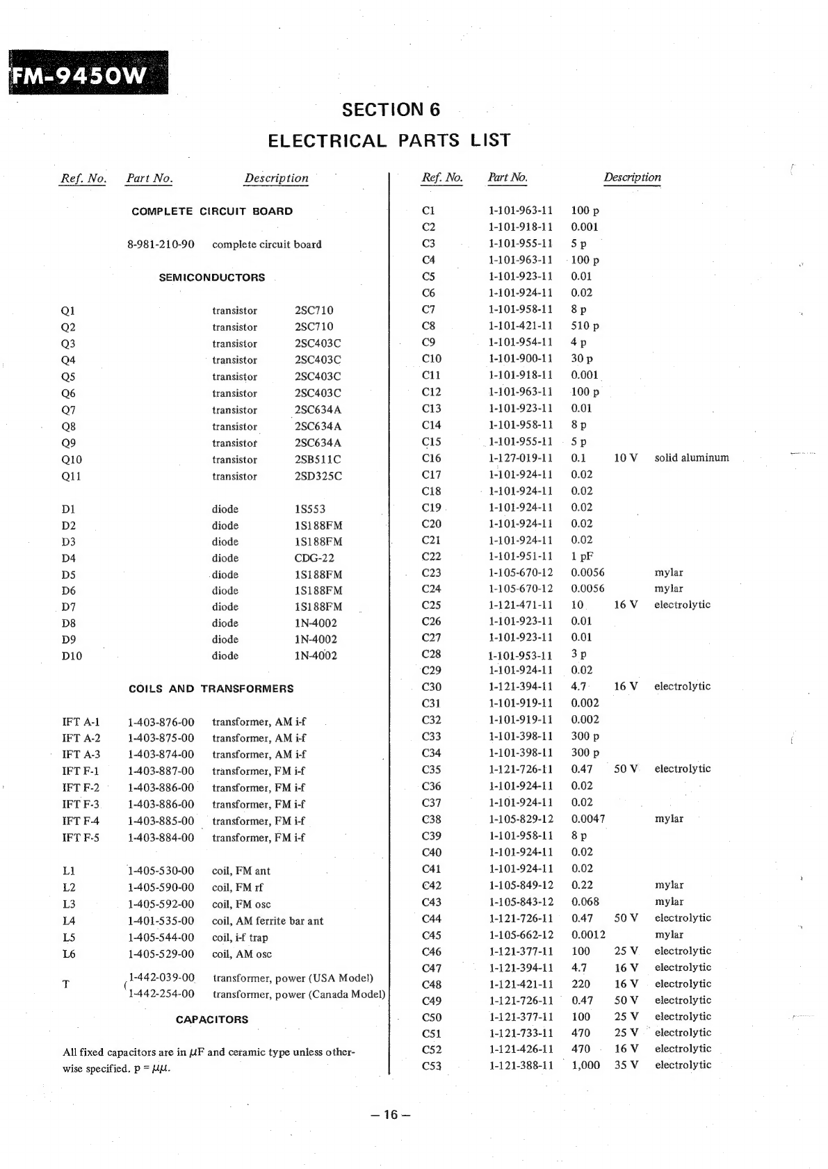
Sony TFM-9450W User manual

Circuit:
Frequency
Ranges:
Intermediate
Frequencies:
Antennas:
Sensitivity
at
50
mW
output:
Selectivity:
SPECIFICATIONS
11-transistor,
10-diode
2-band
superheterodyne
FM
87.5
~108
MHz
(3.42
~
2.78m)
AM
530
~
1,605
kHz
(566
~
187
m)
FM
10.7
MHz
AM
455
kHz
FM
_
ac
line
antenna,
ext
ant
terminals
provided
AM__
built-in
ferrite
bar
antenna
FM
4.4,2V
(13
cB),
S/N
=
30.dB
AM
89UV/m
(39
dB/m)
maximum
33 dB
at
+
10
kHz
off-resonance
at
1,000
kHz
Canada
Model
:
FM/AM
TABLE
RADIO
Power
Output:
Speaker:
Power
Requirements:
Dimensions:
Weight:
5W
maximum
16
cm
(6)
dia
PM
dynamic,
8
Q
120VAC
60Hz,
15W
365
(w)
x
220
(h)
x
150
(d)
mm
149%
(w)
x
8%
(h)
x
5%
(d)
inches
3.35
kg,
7
lb
6
oz
SERVICE
MANUAL

TABLE
OF
CONTENTS
Section
Title
Page
Specifications
..
2...
ee
1
Hardware
Nomenclature
..........-..20-+-022000-
2
SECTION
1.
OUTLINE
I-l:
-Block:
Diagram:
i.4.
4.4.6
%-$-400
#2
A
kod
%
Ble
eG
ate
is
3
1-2...
“External
View:
<2
<6.
fe-4
a3
Rel
Seok
es
BOT
eel
ae
3
1-3.
Internal
View
.......
sp
eea
a
Cten
ae
sede
eee
pao
es
4
SECTION
2.
DISASSEMBLY
2-1.
Rear
Cover
Removal
...
2...
..
2
eee
ee
ee
5
2-2.
ChassisRemoval
.
.
2.
1...
ee
ee
es
5
2-3.
Dial
Scale
Removal
..
2.5.
1
we ee
tte
wee
ee
pe
5
2-4.
BAND
and
LOUDNESS
Switches’
Bracket
Removal
........
6
2-5.
Dial
Cord
Stringing
.
2...
es
6
SECTION
3.
CIRCUIT
ADJUSTMENTS
3-1.
Test
Equipment/Tools
Required
..
12...
2.0.2.0.
ee
eee
7
3-2.
FM
I-f
Alignment..........
et
Sie.
ROS
galt
iigiadt
Beis
Bs
Ge
Bens
se
fi
.
3-3.
FM
Frequency
Coverage
Adjustment
............002-.
7
3-4.
FM
Tracking
Adjustment
...........
0-22
eee
eee
7
3-5.
AM
I-f
Alignment.
2...
2
0.
ee
8
3-6.
AM
Frequency
Coverage
Adjustment
........-.--.--005
8
3-7.
AM
Tracking
Adjustment
...........
00-2
eee
eee
8
SECTION
4.
SCHEMATIC
AND
MOUNTING
DIAGRAMS
4-1.
Schematic
Diagram
.
2
2.
1
ee
ee
ee
9
4-2.
Mounting
Diagram
—
Conductor
Side-
..
2...
..
ee
eee
11
SECTION
5.
EXPLODED
VIEW
AND
PACKING
5<1..
Exploded
View
2... secs
u
we
Gta
es
ele
eR
ee
a
13
5-23.
Packing...
da04
ab
Bia
Cea
he
bene
Oia
ALS
gh
ae
ee
es
Be
as
15
SECTION
6.
ELECTRICAL
PARTS
LIST
.............0...06.
16
—
Hardware
Nomenclature
Pan
Head
Screw
SC
—
Set
Screw
Pan
Head
Screw
E
--
Retaining
Ring
(E
Washer)
with
Spring
Washer
WwW
Washer
Flat
Countersunk
Head
Screw
..
.
SW
Spring
Washer
LW
Lock
Washer
Binding
Head
Screw
:
N
Nut
Oval
Countersunk
Head
Screw
..
—
Example
—
Type
of
Slot
Truss
Head
Screw
®
P
3x10
.
.
ke
Round
Head
Screw
signal
j
Diameter
in
mm
(D)
!---4
Flat
Fillister
Head
Screw
Type
of
Head
od
Note:
All-screws
in
the
set
are
Phillips
type
(cross
recess
type)
unless
otherwise
indicated.
(—):
slotted
head
‘
=
2
sae

SECTION
1
OUTLINE
1-1.
BLOCK
DIAGRAM
FM
_EXT
AFC
ANTENNA
759%
04,
Q5,
06
FM/AM
IF
AMP
Q3
AM
CONV
S3
:
a.
8.
a9
Q10,
Qi1
SP.
AF
AMP
3
POWER
AMP
82
VRI
x
:
TONE
‘
71,
\
D9,
D10
POWER
RECT
AC
LINE
ANT
Fig.
1-1,
1-2.
EXTERNAL
VIEW
X-39801-03-0
knob
ass’y,
VOLUME
X-39801-03-0
knob
ass’y,
TONE
3-844-321-00
knob,
BAND
3-844-321-00
knob,
LOUDNESS
X-39801-02-0
knob
ass’y,
TUNING
Fig.
1-2.
_TFM-9450W
IFM-9450W
1-3.
INTERNAL
VIEW
1-224-163-00
(USA
Model)
1-224-354-00
(Canada
Model}
resistor,
variable,
50
k
(A);
VOLUME
control
1-224-164-00
resistor,
variable,
10
k
(A);
TONE
control
3-980-120-00
heat
sink
1-536-425-00
terminal;
GROUND-75
Q,
FM
EXT
ANTENNA
3-980-024-00
plate,
ac
line
ant
Fig.
1-3.
1-502-425-00
speaker,
8
Q)
1-442-039-00
(USA
Model)
1-442-254-00
(Canada
Mode!)
transformer,
power
(T)

TFM-9450W
SECTION
2
DISASSEMBLY
2-1.
REAR
COVER
REMOVAL
Remove
rear
cover
in
the
numerical
order
shown
in
Fig.
2-1
below.
Remove
rear
cover
in
the
direction
shown
f
by
the
arrow.
washer,
plain;
#3
mm
dia
Remove
two
screws
and
two
plain
washers.
P3x8
Fig.
2-1.
2-2.
CHASSIS
REMOVAL
Remove
chassis
in
the
numerical
order
shown
below.
@
Remove
rear
cover
as
shown
in
Fig.
2-1
above.
@
Pull
off
VOLUME,
TONE
and
TUNING
knob
assemblies,
BAND
and
LOUDNESS
knobs
shown
in
Fig.
2-2
below.
VOLUME
and
TONE
.
knob
assemblies
TUNING
knob
ass’y
BAND
and
LOUDNESS
knobs
Fig.
2-2.
«screw,
machine;
G)
Remove
two
machine
screws,
P
3x
8
(black).
@
Remove
_two
self-tapping
screws,
P
3
x
8
(black).
©Take
out
chassis
in
@Unsolder
black
pve
wire.
the
direction
shown
by
the
arrow.
Fig.
2-3.
2-3.
DIAL
SCALE
REMOVAL
Remove
dial
scale
in
the
numerical
order
shown
below.
@
Remove
chassis
as
shown
in
2-2
above.
Take
out
dial
scale
in
the
direction
shown
by
the
arrow.
Fig.
2-4.
Note:
Voltage
checking
and
parts
replacement
can
be
performed
without
removing
cir-
cuit
board.
TFM-9450W
@
Remove
two
machine
screws,
P
3x
8.
2-4.
BAND
AND
LOUDNESS
SWITCHES’
BRACKET
REMOVAL
Remove
BAND
and
LOUDNESS
switches’
bracket
in
the
numerical
order
shown
below.
@
Remove
chassis
as
outlined
in
2-2
above.
@
Remove
machine
screw,
P 3
x
6.
screw,
machine;
P3x6é
\
©=
@
Remove
BAND
and
LOUDNESS
switches’
bracket
in
the
direction
shown
by
the
arrow.
2-5.
DIAL
CORD
STRINGING
1.
Make
a
dial
cord
assembly
shown
in
Fig.
2-6
below.
drum,
dial
oe
spring,
dial
cord
cord,
dial;
0.5
mm
dia
$i
36”
(915
mm)
Fig.
2-6.
2.
String
the
dial
cord
in
the
numerical
order
shown
in
Fig.
2-7
below.
dial
drum
at
fully
clockwise
position
Fig.
2-7.
3.
Set
the
tuning
shaft
to
fully
counterclockwise
position.
4.
Set
the
dial
pointer
ass’y
on
the
dial
cord
so
that
the
dial
pointer
places
on
the
mark
“0”
of
the
logging
scale,
and
fix
the
dial
pointer
ass’y
on
the
dial
cord
with
a
small
amount
of
lock
paint
as
shown
in
Fig.
2-8
below.
cord,
dial
Apply
a
small
amount
of
lock
paint
here.
pointer
ass’y,
dial
Fig.
2-8.

-TFM-9450W
—
TFM-9450W.
SECTION
3
|
CIRCUIT
ADJUSTMENTS
3-1.
TEST
EQUIPMENT/TOOLS
REQUIRED
3-4.
FM
TRACKING
ADJUSTMENT
3-5.
AM
1-F
ALIGNMENT
*
AM
rf
signal
generator
;
*
FM
rf
signal
generator
Test
Setup:
Same
as
Fig.
3-1.
;
Test
Setup:
*
Loop
antenna
VOM
*
VOM
AM
ff
signal
loop
antenna
:
0.5~5VAC
*
generator
test
set
Alignment
screwdriver
Rf
Signal
Rf
Signal
Receiver
Generator
Generator
Dial
:
Coupling
Frequency
Setting
Preparation:
Direct
Minimum
Pitch
of
FM
;
P
connection
86.5
MHz
frequency
rf
coil
L2
rene
Saga
FM
t
di
-
to
FM
EXT
Maxi
FM
rf
trim
Repeat
sausdiene
tae
ot
tives
aan
ding
AM
rf
signal
generator
modulation:
aximum
r
:
ijustmen
ree
times
endin|
16
&
ANTENNA
110MHz
frequency
mer
TCL
with
TC].
Fix
L2
with
wax.
]
kHz,
30%
terminals
aa
AM
rf
signal
generator
output
level:
Usable
lowest
possible.
:
FM
rf
signal
generator
modulation:
Fig.
3-3.
Speaker
terminals
Rf
Signal
Rf
Signal
Receiver
Generator
Generator
Diat
Adjust
Remarks
Coupling
Frequency
Setting
400
Hz,
+
22.5
kHz
deviation
IFT
A-1
Carasot
BAND
selector:
AM
FM
rf
signal
generator
output
level:
:
:
& g
.
P
Loop
antenna
455 kHz
No
station,
no
IFT
A-l
ae
for
maximum
meter
Usable
lowest
possible
IFT
A-2
|
See
Fig.
3-3.
cecnapuniice
eae
reading.
FM
rf
signal
generator
coupling:
IFT
A-3
ee
pee
Direct
connection
to
FM
EXT
ANTENNA
terminals.
VOLUME
control
setting:
MAX
TONE
control
setting:
HIGH
LOUDNESS
switch
setting:
OFF
IFT
A-3
3-6.
AM
FREQUENCY
COVERAGE
ADJUSTMENT
Test
Setup:
vom
AM
rf
signal
loop
antenna
0.5~5
VAC
generator
3-2.
FM
1-F
ALIGNMENT
VOM
Test
Setup:
:
IFT
@
$$
og
9572088
_—
Manne
os
-
oan
TN
gnal
0O5~5
VAC
0.002
5
generator
IFT
iA
‘a
A
2001
k
IFT
F-2
IFT
F-3
IFT
F-4
speaker
terminals
5.
Rf
Signal
Rf
Signal
Receiver
IFT
F-5
Generator
Generator
Dial
Coupling
Frequency
Setting
FM
EXT
ANTENNA
terminals
BAND
selector:
AM
Adjust
for
maximum
meter
reading.
Repeat
adjustment
two
or
three
times
ending
with
TC4.
speaker
terminals
Fig.
3-1.
_—
:
520
kH
Minimum
Core
of
AM
osc
~
Stee
ae
@
frequency
coil
L6
i
1
i
Loop
antenna
Fig.
3-4.
Adjustment
locations
See
Fig.
3-4.
SAE
Ear
1,680
kHz
eecnancy
~
Rf
Signal
Receiver
Generator
Dial
Frequency
Setting
Cores
of
IFT
F-1
Test
setup:
See
Fig.
3-1.
10.7
MHz
No
station,
with
FM
no
beating
IFT
F-2
BAND
selector:
FM
‘
ook
IFT
F-3
Adjust
for
maximum
meter
reading.
modulation
Position
IFT
F-4
Repeat
adjustment
two
or
three
times.
3-7.
AM
TRACKING
ADJUSTMENT.
IFT
F-5
Test
Setup:
VOM
No
input
Test
setup:
See
Fig.
3-2.
Signal
:
Adjust
for
‘*O0
VDC”
meter
reading.
AM
rf
signal
loop
antenna
0.5
~5
VAC
(noise
oniy)
:
generator
test
set
Or
3-3.
FM
FREQUENCY
COVERAGE
ADJUSTMENT
O
Test
Setup:
Same
as
Fig.
3-1.
speaker
terminals
Rf
Signal
Rf
Signal
Receiver
Rf
Signat
Rf
Signal
Receiver
Generator
Generator
Dial
Adjust
Remarks
Generator
Generator
Dial
Adjust
Remarks
Coupling
Frequency
Setting
Coupling
Frequency
Setting
Direct
Minimum
Pitch
of
FM
x
-
Tune
in
bis
BAND
selector:
AM
connection
86.5
MHz
frequency
osc
coil
L3
BAND
selector:
FM
di
620
kHz
620
kHz
ey
AM
Adjust
for
maximum
meter
to
FM
EXT
~
-
Adjust
for
maximum
petra
ing.
a
Lod
antenna
signal
ant
col
reading.
ANTENNA
110
MHz
Maximum
FM
osc
trim-
Repeat
adjustment
two
or
three
times
ending
See
Fig.
3-5.
-
Repeat
adjustment
two
or
:
frequency
mer
TC2
with
TC2.
Fix
L3
with
wax.
Tune
in
, :
3
‘i
terminals
AM
ant
trimmer
three
times
ending
with
TC3.
1,400
kHz
1,400
kHz
Fix
L4
wi
signal
TC3
ix
L4
with
wax.

4-1.
SCHEMATIC
DIAGRAM
dex
22k
TC3
QI
2Sc710
FM
RF
AMP
(1.85V)
SECTION
4
SCHEMATIC
AND
MOUNTING
DIAGRAMS
Q2
2SC710
FM
CONV
C9
4p
R28
2.7k
L4
AM
ANT
COIL
R26
100
“5.0
Q3
25C403C
AM
CONV
R27
750
D2
!SI88FM
LIMITER
L6
AM
OSC
COIL
ol
DI
1$553
.
FM
AFC
D7
ISIB8FM
AM
AGC
TFM-9450W
Q4
2SC403¢
FM/AM
IF
AMP
|
r
1
Q4
i
De
ap}
«)
=
=|
lt
i 1
K1.0V)
dav)
2.5Vrange
{7.6V
<8,
5V.
Y
(0.47V)
™
<0.57)
TFM-9450W
Q5
25C403C
D3
1SIBBFM
04
CDG-22
FM/AM
IF
AMP
2
LIMITER
Toxo
47/\6V
R!I6
2.2k
(8.6V)
<a,7\)
RS!
3.9k
|
—~——
25.5V
C54
0.0!
Q6
2SC403C
D5,D6
ISI88FM
FM
IF
AMP
3
FM
DET
(7.5V)
7V)
<egvy.
HEURES
_
EL
Fo.
pS
Ret
lk
R23
5.6k
l
C53
DIO
1000
Tose.
'T
470/16V
C55
001
D8
IN-4002
'Q7
2SC634A
AF
AMP
I
Fig.
4-1.
Q8
2SC634A
AF
AMP
2
AF
AMP
3
Q9
2SC634A
Qi!
2SD325¢
D9,DIO
IN-4002
QIO
2SB5IIC
;
POWER
RECT
POWER
AMP
Note:
1.
All
fixed
resistors
are
in
Q,
+5
%,
%
W.
2.
All
fixed
capacitors
are
in
UF
unless
otherwise
specified.
3.
Voltage
readings
are
taken
with
a
20
kQ./V
DC
VOM
with
reference
to
heavy
lines.
Those
shown
in
( )
’
indicate
readings
on
FM,
in
<
>on
AM,
others
are
common.
4.
Capacitors
marked
with
A
are
built
in
i-f
transformers.
~10—
e@=
{20V
AC
AC
=
LINE
ANT

TFM-9450W
_TFM-9450W
4-2...
MOUNTING
DIAGRAM
—
Conductor
Side
—
Transistor
Location
Q1:
6E
Q7:
3D
Q2:
6G
as:
3D
Q3:
5E
ag:
3D
Q4:
5G
Q10:
5C
Q5:
4F
Qi1:
4¢
J
}
i
(
|
‘
Qé6:
3F
.f
7.5)
|
.
gave!
remap
Q1,
Q2:
28C710
D1:
18553
7
R
i
abba
3
d
-
er
€
4
%
ece
;
-———
Q3-Q6:
2SC403C
D2-D7:
18788
Q7-Q9:
2SC634A
chassis
PNK
[vouune}
c
(7.7V)
HO)
<B.6V)
E
{0,85V)
.
&c
8
<1.0V>
(0,65V)
<0,7V>
2.5V
range
Q10:
2SB511C
D8-D10:
1N-4002
:
be
chassis
(7.6V}
<8.5V)
(0,47V)}
<0.57V)
7.9V
(1.0V)
<L.EY>
(7.9V}
(1.85V)}
(0.85y)
2.5V
range
Note:
R58
marked
with
#
is
mounted
on
the
conductor
side.
(0.86V)
(0.75y)
chassis
Gamay
PLI
L4.
AM
ANT
cor
{
FM
EXT
ANT
ar
Fig.
4-2.
|
WH
Ae
rere
nee

TFM-9450W
SECTION
5
EXPLODED
VIEW
AND
PACKING
5-1.
EXPLODED
VIEW
7-623-208-11
washer,
plain;
3
mm
dia
3-980-024-00
7-684-013-00
plate,
ac
line
ant
nut,
3mm
dia
A
3-980-025-00
[
oe
insulator,
ac
line
ant
plate
1-534-853-00
rum
a
8-987-210-90
1-151-261-00
cord,
ac
power
7-621-259-62
complete
eireut
t
board
capacitor,
tuning
screw,
machine;
K
2.6
x
8
i
:
.
7:682-147-03
_—
7-633-120-42
cord,
dial;
0.5
mm
dia
3-980-029-00
yo
strain
relief
/:
bo
1-442-039-00
(USA
Model}
1-442-254-00
(Canada
Model}
transformer,
power
{T}
ut,
3mm
dia
7-682-247-03
screw,
machine;
K
3
x
6
X-39801-01-0
cabinet
ass’y
3-980-023-00
washer,
special.
|
ce
X-39801-81-0
“7
board
ass‘y,
baffle;
including
Pad
|
1-502-425-0
part
marked
with
rig
bd
speaker,
8
Q.
e
:
3-980-112-00
ft
scale,
dial
7-682-148-03
aaa
screw,
machine;
P
3x8
_-
©
3.980-104-00
Pe
4-00,
a
3-980-019-00
emblem,
“SONY
eS
foot,
rubber
|
§
|
-
“_3-980.032.00_7-685-146:06
all
a
Spring,
dial
cord
screw,
self-tapping;
P3
x
8
(black)
TFM-9450W_
3-980-110-00
{USA
Model)
3-980-121-00
(Canada
Model}
cover,
rear
3-844-245-00
{USA
Model}
3-980-040-00
label,
FCC
3-980-039-00
grommet,
rubber
holder,
AM
ferrite
bar
ant
At
7-621-259-22
©.
SL
Screw,
machine;
P
2.6
x
4
ne:
7-685-146-43
screw,
machine;
P
3
x
6
screw,
self-tapping;
P
3
x
&
a
7-682-148-03
screw,
machine;
P
3x
8
7-623-208-11
washer,
plain;
3mm
dia
7-623-208-11
;
7-623-508-11
;
1-401-535-00
3-980-021-00
a
a
aa
MM,
a
al
al
coil,
AM
ferrite
bar
ant
bracket,
power
transformer
———.
7-684-013-00
3-845-828-00
clamp,
wire
7-685-146-43
2
screw,
self-tapping;
P
3
x
&
1-224-163-00
(USA
Model)
1-224-354-00
(Canada
Model)
resistor,
variable,
50
k
(A);
VOLUME
contro!
with
switch
1-224-164-00
tuning
shaft
resistor,
variable,
10
k
(Aj;
TONE
controf
7-623-508-11
lug,
solder;
3
mm
dia
7-685-146-43
screw,
self-tapping;
P
3
x
8
“s
7-685-146-05
i
¥
screw,
self-tapping;
P
3
x
8
(black)
yo80
120-00
heat
sink
3-980-041-00
collar.
3980-042-00
insulator,
mica
ea
~~
X-39800-05-0
transistors
chassis
ass’y
Q10,
11
7-621-843-21
‘oa
plate,
back
:
screw,
wood:
R
3.1
x
10
SO
<
.
a
-
ea
parts
of
variable
‘<
.
Soe
7-685-146-43
3-980-030-00
<
,
tos,
screw,
self-tapping;P
3x8
shaft,
tuning
+
yes
1-582-188-00
\
See
t
“SL
3-980-023-00
circuit
board,
BAND
selector
slide
switch
bee
ae
:
H
washer,
special
1-516-232-00
3
a
8
H
.
Switch,
slide;
BAND
selector
‘
;
:
a
1:516-231-00
1
t
p
switch,
slide;
LOUDNESS
I
t
H
U
K
uw
7-685-145-43
\
Ng
screw,
self-tapping;
P
3
x
6
|
ie
BB
7-682-147-0037
it
.
=
screw,
machine;
P'3x
6
|
|
:
csp
COUN
76.0
.
3-980-022-00
°°.
terminal;
UND-78
Q,
washer,
special
~*:
FM
EXT.
:
ANTE!
NNA
S
X-39801-03-0
:
knob
ass'y,
VOLUME
7-682-150-03
3-980-020-00
screw,
machine;-P
3
x
12
bracket,
terminal
board
X-39801-03-0
\
knob
ass’y,
TONE
3-980-033-00
3-980-019-00
it
foot,
rubber
3-844-321-00
label,
caution
X-39801-02-0
knob,
LOUDNESS
knob
ass‘'y,
TUNING
[WY
3980-022-00
7-621-843-21
3-844-321-00
Washer,
special
screw,
wood;
R
3.1.x
10
knob,
BAND
’
7-682-150-03
3-844-246-00
;
X-39801-82-0
screw,
machine;
P
3
x
12
Jabel,
serial
number
panel
ass‘y,
control
Pee
ce
3-980-111-00
:
Note:
bracket,
BAND
and
LOUDNESS
switches
©
Items
without
part
number
and
description
7-621-259-22
are
not
available.
screw,
machine;
P'
2.6
x
4
©
All
screws
are
Phillips
(cross
recess)
type
unless
otherwise
noted.
(—)
=
slotted
head
Fig.
5-7.
—14-—

5-2.
PACKING
3-980-115-00
cushion,.styrol
foamed
3-980-119-00
manual,
instruction
3-980-118-00
bag,
polyethylene
3-980-115-00
cushion,
styrol
foamed
3-980-116-00
carton,
individual
Note:
-
©
Items
without
part
number
and
description
Fig.
5-2.
are
not
available.
S45
=

SECTION
6
ELECTRICAL
PARTS
LIST
Ref.
No.
Part
No.
Description
;
Ref.
No.
Part
No.
Description
COMPLETE
CIRCUIT
BOARD
Cl
j-101-963-11
100
p
C2
1-101-918-11
0.001
8-981-210-90
complete
circuit
board
C3
1-101-955-11
Sp
|
C4
1-101-963-11
-100p
SEMICONDUCTORS
C5
1-101-923-11
0.01
C6
1-101-924-11
0.02
Qi
transistor
28C710
C7
1-101-958-11
8p
Q2
transistor
2SC710
C8
1-101-421-11
510p
Q3
transistor
2SC403C
co
1-101-954-11
4p
Q4
transistor
28C403C
C10
1-101-900-11
30p
Q5
transistor
2SC403C
Cil
1-101-918-11
0.001
Q6
transistor
28C403C
Ci2
1-101-963-11
100
p
Q7
transistor
—28C634A
C13
1-101-923-11
0.01
Q8
transistor
2SC634A
C14
1-101-958-11
8p
Q9
transistor
2SC634A
C15
_1-101-955-11
-
5p
Q10
transistor
2SBS511C
C16
1-127-019-11
0.1
10V
©
solid
aluminum
Qlil
transistor
2SD325C
Ci7
1-101-924-11
0.02
C18
1-101-924-11
0.02
DI
diode
18553
C19
1-101-924-11
0.02
D2
diode
1S188FM
C20
1-101-924-11
0.02
D3
diode
1S188FM
C2i
1-101-924-11
0.02
D4
diode
CDG-22
C22
1-101-951-11
1
pF
DS
diode
1S188FM
C23
1-105-670-12
0.0056
mylar
D6
diode
1S188FM
C24
1-105-670-12
0.0056
mylar
D7
diode
1S188FM
C25
1-121-471-11
10
16V__
electrolytic
D8
diode
1N-4002
C26
1-101-923-11
0.01
D9
diode
1N-4002
C27
1-101-923-11
0.01
D10
diode
1N-4002
C28
1-101-953-11
3p
C29
1-101-924-11
0.02
COILS
AND
TRANSFORMERS
C30
1-121-394-J1
4.7
16
V__
electrolytic
C31
1-101-919-11
0.002
IFT
A-1
1-403-876-00
transformer,
AM
i-f
C32
1-101-919-11
0.002
IFT
A-2
1-403-875-00
transformer,
AM
i-f
C33
1-101-398-11
300p
IFT
A-3
1-403-874-00
transformer,
AM
i-f
:
C34
1-101-398-11
300p
IFT
F-1
1-403-887-00
—
transformer,
FM
i-f
C35
1-121-726-11
0.47
50V
__
electrolytic
IFT
F-2
1-403-886-00
transformer,
FM
i-f
C36
1-101-924-11
0.02
IFT
F-3
1-403-886-00
transformer,
FM
i-f
C37
1-101-924-11
0.02
IFT
F-4
1-403-885-00
transformer,
FM
if
C38
1-105-829-12
0.0047
mylar
IFT
F-5
1-403-884-00
transformer,
FM
i-f
C39
1-101-958-11
8p
C40
1-101-924-11
0.02
Li
‘1-405-530-00
coil,
FM
ant
C41
1-101-924-11
0.02
L2
1-405-590-00
coil,
FM
rf
C42
1-105-849-12
0.22
mylar
L3
1-405-592-00
coil,
FM
osc
C43
1-105-843-12
0.068
mylar
14
1-401-535-00
coil,
AM
ferrite
bar
ant
C44
1-121-726-11
0.47
50V__
electrolytic
LS
1-405-544-00
coil,
i-f
trap
C45
1-105-662-12
0.0012
mylar
L6
1-405-529-00
coil,
AM
osc
C46
1-121-377-11
100
25
V._
electrolytic
C47
1-121-394-11
4.7
16V__
electrolytic
i
cee
eee
Dewey
ie
ei
C48
1-121-421-11
220
16V__
electrolytic
mp
swer
Canada
Moded
49
1-121-726-11
0.47
50V__
electrolytic
CAPACITORS
‘
C50
1-121-377-11
100
25
V_—
electrolytic
C51
j-121-733-11
470
25
V
©
electrolytic
All
fixed
capacitors
are
in
UF
and
ceramic
type
unless other-
C52
1-121-426-11
470
16V__
electrolytic
wise
specified.
p
=
MH.
C53
1-121-388-11
1,000
35V__
electrolytic
—~16—

_
TFM-9450
Ref.
No.
Part
No.
Description
Ref.
No.
Part
No.
Description
C54
1-102-317-11
0.01
R33
1-242-667-11
560
C55
1-102-317-11
0.01
R34
1-242-685-11
3.3k
C56
1-101-421-11
510
p
R35
1-242-689-11
4.7k
C57
1-101-923-11
0.01
R36
1-242-689-11
4.7
C58
1-105-821-12
0.001
mylar
R37
1-242-725-11
150k
C59
1-101-875-1136
p
R38
1-242-670-11
750
R39
1-242-681-11
2.2k
TC1-TC4
;
,
R40
1-242-679-11
1.8k
Ceres
1151-261-00
tuning
R41
1-244-641-1147
R42
1-242-715-11
56k
RESISTORS
R43
1-242-693-11
6.8k
R44
—s'1-242-689-11
4.7
All
fixed
resistors
are
in
92,
+5
%,
'%
W
carbon
film
type.
R45
1-244-863-11
390
ww
k=
1,000,
M
=
1,000,000.
R46
1-244-857-11
220
%W
R47
1-242-631-1118
Ri
1-242-673-11
1k
R48
1-244-802-1111
“%W
R2
1-242-737-11
470k
R49
1-244-802-1111
%W
R3
1-244-681-11
2.2
k
R50
1-242-685-11
3.3k
R4
1-242-681-11
2.2
k
R51
1-242-687-11
3.9k
RS
1-242-673-11
1k
R52
1-242-742-11
750k
R6
1-242-743-11
820k
R53
1-242-667-11
560
R7
1-242-649-11
100
R54
1-242-673-11
1k
R8
1-244-673-11
1k
RSS
1-242-737-11
470k
Ro
1-242-641-1147
R56
1-202-657-11
3.3M
%W
composition
R10
1-244-741-11
680k
R57
1-242-694-11
7.5k
Ril
1-244-673-11
1k
R58
1-242-649-11
100
R12
1-242-673-11
1k
.
R59
1-242-633-1122
R13
1-244-695-11
8.2k
ao
arora
VR1
1-224-164-00
variable,
10
k
(A);
TONE
‘control
ee
a
oa
1-224-163-00
variable,
50k
(A);
VOLUME
control
R16
1-242-681-11
2.2
k
with
switch
(USA
Model)
R17,
1-244-673-11
1k
a
1-224-354-00
variable,
50
k
(A);
VOLUME
control
R18
1-242-681-11
22k
with
switch
(Canada
Model)
R19
1-242-694-11
7.5k
Misherv
ANEOUS
R20
1-244-673-11
1k
se
neta:
oe
PLI
1-518-177-00
lamp,
pilot
aes
ety
PL2
1-518-177-00
lamp,
pilot
R23
1-242-691-11
5.6
k
BA
Pee
a
ek
SP
1-502-425-00
speaker,
8
2
R25
1-242-743-11
820k
Sa
ee
ae
si
1-516-232-00
switch,
slide;
BAND
selector
ie
eee
ae
$3
1-516-231-00
switch,
slide;
LOUDNESS
R28
1-242-683-11
2.7k
1-534-853-00
-
cord,
ac
power
R29
1-242-697-11
-
10k
1-536-425-00
terminal;
GROUND-75
2,
R30
1-244-719-11
82k
FM
EXT
ANTENNA
R31
peas
1-582-188-00
circuit
board,
band
selector
slide
R32
1-242-705-11.
22k
switch
sc
ee
Other manuals for TFM-9450W
1
Table of contents
Other Sony Radio manuals

Sony
Sony ICF-T30 User manual

Sony
Sony XDR-S16DBP User manual

Sony
Sony ICF-P26 Instruction Manual

Sony
Sony ICF-40 User manual

Sony
Sony ICF-SW7600 User manual

Sony
Sony ICF-SW7600GR - Portable Radio User manual

Sony
Sony SRF-M90 User manual

Sony
Sony SRF-PSY04 User manual

Sony
Sony ICF-703 User manual

Sony
Sony ICF-B01 User manual
Popular Radio manuals by other brands

Global Sat
Global Sat ICOM IC-SAT100 IRIDIUM PTT Practices Guide

Cambridge Sound Works
Cambridge Sound Works 740 user manual

Silvercrest
Silvercrest SWED 500 A1 User manual and service information

Ruark Audio
Ruark Audio R1 user guide

Basic XL
Basic XL BXL-HDR10 user manual

E-Bench
E-Bench KH 994 owner's manual