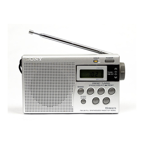
Sony XDR-S1 User manual

1
Ver 1.0 2004. 09
SERVICE MANUAL
AEP Model
UK Model
XDR-S1
SPECIFICATIONS
Time display
UK 12-hour system
Other countries/regions 24-hour system
Frequency range
Band Frequency Channel step
DAB (L-Band) 1452.960
– 1490.624 MHz
DAB (Band-III) 174.928
– 239.200 MHz
FM 87.5 – 108 MHz 0.05 MHz
MW 531 – 1,602 kHz 9 kHz
LW 153 – 279 kHz 3 kHz
Speaker: 8 cm (3 1/4 inches) dia., 3.2 Ω
Power output: 2.3 W+2.3 W (at 10% harmonic distortion)
Output: Headphone jack (stereo mini jack)
Power requirements: 230 V AC, 50 Hz
Power consumption: 13 W
Dimensions: Approx. 320 ×142 ×154 mm (w/h/d)
(Approx. 12 3/4 ×5 5/8 ×6 1/8 inches) incl.
projecting parts and controls
Mass: Approx. 2.5 kg (5 lb 8 oz)
Supplied accessories: AC power cord (1),
Remote control (RMT-CS1AD) (1)
Design and specifications are subject to change
without notice.
Sony Corporation
Personal Audio Company
Published by Sony Engineering Corporation
9-879-193-01
2004I04-1
© 2004. 09
DAB/FM/MW/LW DIGITAL RADIO
www.freeservicemanuals.info
23/7/2013
World of free manuals

2
XDR-S1
SAFETY-RELATED COMPONENT WARNING!!
COMPONENTS IDENTIFIED BY MARK 0OR DOTTED LINE
WITH MARK 0ON THE SCHEMATIC DIAGRAMS AND IN
THE PARTS LIST ARE CRITICAL TO SAFE OPERATION.
REPLACE THESE COMPONENTS WITH SONY PARTS WHOSE
PART NUMBERS APPEAR AS SHOWN IN THIS MANUAL OR
IN SUPPLEMENTS PUBLISHED BY SONY.
Flexible Circuit Board Repairing
•Keep the temperature of the soldering iron around 270˚C during
repairing.
•Do not touch the soldering iron on the same conductor of the
circuit board (within 3 times).
•Be careful not to apply force on the conductor when soldering
or unsoldering.
Notes on Chip Component Replacement
•Never reuse a disconnected chip component.
•Notice that the minus side of a tantalum capacitor may be dam-
aged by heat.
•UNLEADED SOLDER
Boardsrequiring useof unleadedsolder areprinted withthe lead-
free mark (LF) indicating the solder contains no lead.
(Caution:Some printed circuitboards maynot comeprinted with
the lead free mark due to their particular size.)
: LEAD FREE MARK
Unleaded solder has the following characteristics.
•Unleaded solder melts at a temperature about 40°C higher
than ordinary solder.
Ordinary soldering irons can be used but the iron tip has to
be applied to the solder joint for a slightly longer time.
Soldering irons using a temperature regulator should be set
to about 350°C.
Caution: The printed pattern (copper foil) may peel away if
the heated tip is applied for too long, so be careful!
•Strong viscosity
Unleaded solder is more viscous (sticky, less prone to flow)
than ordinary solder so use caution not to let solder bridges
occur such as on IC pins, etc.
•Usable with ordinary solder
It is best to use only unleaded solder but unleaded solder
may also be added to ordinary solder.
TABLE OF CONTENTS
1. GENERAL
2. DISASSEMBLY
2-1. Cabinet (Rear) Assy ............................................................ 4
2-2. Wires ................................................................................... 5
2-3. Cabinet Upper Assy ............................................................ 5
2-4. Key Board ........................................................................... 6
2-5. Tuner Board......................................................................... 6
2-6. Micon Board ....................................................................... 7
2-7. Power Board, Jack Board ....................................................7
3. ELECTRICAL ADJUSTMENTS................................... 8
4. DIAGRAMS
4-1. Printed Wiring Board –Tuner Section– ............................. 10
4-2. Printed Wiring Boards –Micon Section– .......................... 11
4-3. Schematic Diagram –Tuner, Micon Section– ................... 12
4-4. Printed Wiring Boards –Audio, Power Supply Section– .. 13
4-5. Schematic Diagram –Audio, Power Supply Section–....... 14
5. EXPLODED VIEWS
5-1. Cabinet (Rear) Section ...................................................... 17
5-2. Cabinet Front Section........................................................ 18
5-3. Chassis Section ................................................................. 19
6. ELECTRICAL PARTS LIST ........................................ 20
www.freeservicemanuals.info
23/7/2013
World of free manuals

3
XDR-S1
SECTION 1
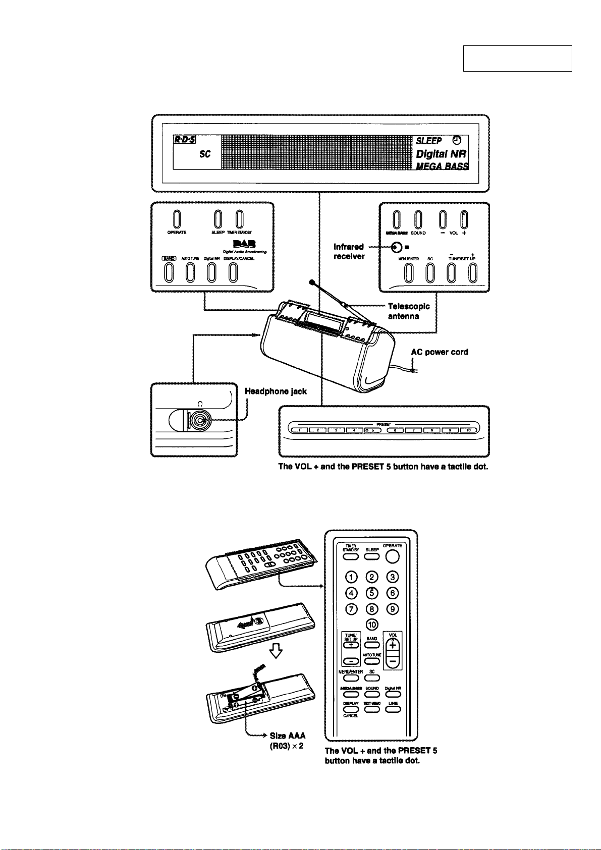
GENERAL This section is extracted
from instruction manual.
• LOCATION OF CONTROLS
www.freeservicemanuals.info
23/7/2013
World of free manuals

4
XDR-S1
• The equipment can be removed using the following procedure.
SECTION 2
DISASSEMBLY
2-1. CABINET (REAR) ASSY
Note : Follow the disassembly procedure in the numerical order given.
2-1. CABINET (REAR) ASSY
(Page 4)
2-2. WIRES
(Page 5)
SET
2-3. CABINET UPPER ASSY
(Page 5)
2-4. KEY BOARD
(Page 6)
2-5. TUNER BOARD
(Page 6)
2-6. MICON BOARD
(Page 7) 2-7. POWER BOARD,
JACK BOARD
(Page 7)
1
net assy
2
four
screws
(+
BV tapping (B3)
)
3
four
screws
(+
BV tapping (B3)
)
4
two
screws
(+
BV tapping (B3)
)
5
two
screws
(+
BV tapping (B3)
)
6
cabinet (rear) assy
four claws
www.freeservicemanuals.info
23/7/2013
World of free manuals

5
XDR-S1
2-3. CABINET UPPER ASSY
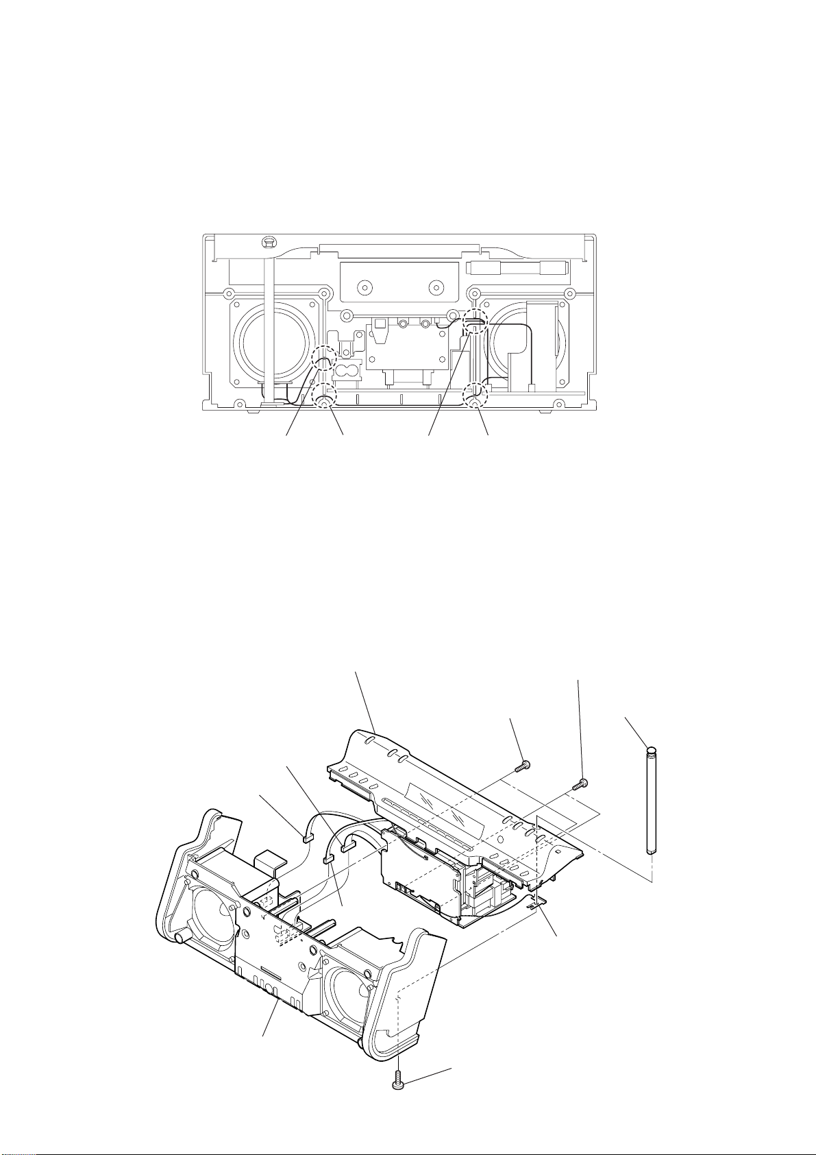
2-2. WIRES
Put flat cable and wires between the cabinets and push them in the
grooves located at A to D in the figure to prevent disconnection
before assembling the set.
AB CD
front side
6
two
screws
(+
BV tapping (B3)
)
7
two
screws
(+
BV tapping (B3)
)
terminal (antenna)
cabinet front assy
8
cabinet upper assy
4
screw
(M3x6 lock ace)
5
telescopic antenn
a
1
CN302 (4P)
2
CN304 (9P)
3
CN301 (6P)
www.freeservicemanuals.info
23/7/2013
World of free manuals

6
XDR-S1
2-5. TUNER BOARD
2-4. KEY BOARD
2
two
screws
(+
P tapping (B2.6)
)
3
two
screws
(+
P tapping (B2.6)
)
5
three
screws
(+
P tapping (B2.6)
)
6
five
screws
(+
P tapping (B2.6)
)
4
cabinet upper assy (SVX)
7
KEY board
1
CN702 (4P)
4
two
screws
(+
P tapping (B2.6)
)
3
two
screws
(+
P tapping (B2.6)
)
5
1
CN501
2
CN504 (3P)
8
CN502 (22P)
9
TUNER board
6
CN503 (9P)
7
CN704 (6P)
www.freeservicemanuals.info
23/7/2013
World of free manuals

7
XDR-S1
2-6. MICON BOARD
2-7. POWER BOARD, JACK BOARD
1
screw
(+
P tapping (B2.6)
)
2
helical antenna
4
three
screws
(+
P tapping (B2.6)
)
5
three
screws
(+
P tapping (B2.6)
)
6
MICON board
3
Remove the five solderings.
red
greenblackyellow
natural
claw
claw
1
two
screws
(+
PWH tapping (B2.6)
)
2
JACK board
chassis
6
two
screws
(+
BV tapping (B3)
)
7
POWER board
5
two
screws
(+
BV tapping (B3)
)
3
two
screws
(+
BV tapping (B3)
)
4
bracket (AC inlet)
www.freeservicemanuals.info
23/7/2013
World of free manuals

8
XDR-S1 SECTION 3
ELECTRICAL ADJUSTMENTS
TRACKING ADJUSTMENT
This set has the calibration function for tracking adjustment. It is
calibrated on each of LW and MW bands using frequencies at 7
points or 9 points.
Setting:
BAND: MW or LW
• LW
1. With the power off, press the 4 keys: [TIMER STANDBY], [SC],
0and [DISPLAY] simultaneously for 3 seconds. The LCD
display shows “Calibration Mode” on the top and “LW MW
EXIT” on the bottom.
Put the lead-wire
antenna close to
the set.
AM RF signal
generator
30% amplitude
modulation by
400 Hz signal
Calibration Mode
LW MW EXIT
Calibration
153kHz
2. Select “LW” using the TUNE/SET UP [+]/[--] key, and press
the [MENU/ENTER] key.
3. The LCD display shows “Calibration” on the top and the
frequency at 1st point “153 kHz” on the bottom.
4. Set the output frequency of the signal generator to 153 kHz.
5. When adjustment at 1st point is completed (it takes for about 3
seconds), press the [MENU/ENTER] key.
6. Repeat steps 3 to 5 until adjustment at 2nd point to 7th point is
completed.
Frequency at each point:
1st point: 153 kHz
2nd point: 162 kHz
3rd point: 174 kHz
4th point: 186 kHz
5th point: 195 kHz
6th point: 243 kHz
7th point: 279 kHz
7. Once adjustment at all the points is completed, the LCD display
shows “Complete Cancel” on the top. Select either of the
followingoptions usingtheTUNE/SET UP[+]/[--] keyand press
the [MENU/ENTER] key.
Complete: Writes the data and returns to the menu.
Cancel: Aborts the data and returns to the menu.
• MW
1. Select “MW” using the TUNE/SET UP [+]/[--] key, and press
the [MENU/ENTER] key.
2. The LCD display shows “Calibration” on the top and the
frequency at 1st point “531 kHz” on the bottom.
3. Set the output frequency of the signal generator to 531 kHz.
4. When adjustment at 1st point is completed (it takes for about 3
seconds), press the [MENU/ENTER] key.
5. Repeat steps 2 to 4 until adjustment at 2nd point to 9th point is
completed.
Frequency at each point:
1st point: 531 kHz
2nd point: 603 kHz
3rd point: 702 kHz
4th point: 801 kHz
5th point: 900 kHz
6th point: 999 kHz
7th point: 1305 kHz
8th point: 1503 kHz
9th point: 1602 kHz
6. Once adjustment at all the points is completed, the LCD display
shows “Complete Cancel” on the top. Select either of the
following optionsusingtheTUNE/SET UP[+]/[--] key andpress
the [MENU/ENTER] key.
Complete: Writes the data and returns to the menu.
Cancel: Aborts the data and returns to the menu.
• Termination of Adjustment
1. Select “EXIT” using the TUNE/SET UP [+]/[--] key, and press
the [MENU/ENTER] key.
2. The LCD display shows “Please Reset”. Press the [RESET] key
to terminate the Calibration Mode.
www.freeservicemanuals.info
23/7/2013
World of free manuals

99
XDR-S1
XDR-S1
SECTION 4
DIAGRAMS
• CIRCUIT BOARDS LOCATION • NOTE FOR PRINTED WIRING BOARDS AND SCHEMATIC DIAGRAMS
THIS NOTE IS COMMON FOR PRINTED WIRING
BOARDS AND SCHEMATIC DIAGRAMS.
(In addition to this, the necessary note is
printed in each block.)
for schematic diagram:
•All capacitors are in µF unless otherwise noted. (p: pF)
50 WV or less are not indicated except for electrolytics
and tantalums.
•All resistors are in Ωand 1/4W or less unless otherwise
specified.
•C: panel designation.
•A: B+ Line.
•Voltage and waveforms are dc with respect to ground
under no-signal conditions.
no mark : FM
():MW
<>:LW
•Voltagesaretaken witha VOM(Input impedance10 MΩ).
Voltage variations may be noted due to normal produc-
tion tolerances.
•Waveforms are taken with a oscilloscope.
Voltage variations may be noted due to normal produc-
tion tolerances.
•Circled numbers refer to waveforms.
•Signal path.
F: FM
f: MW
E: DAB
j: LW
for printed wiring boards:
•X: parts extracted from the component side.
•Y: parts extracted from the conductor side.
•: Pattern from the side which enables seeing.
(The other layer’s patterns are not indicated.)
Note: The components identified by mark 0or dotted line
with mark 0are critical for safety.
Replace only with part number specified.
Caution:
Pattern face side: Partson thepatternfacesideseen from
(Side B) the pattern face are indicated.
Parts face side: Parts on the parts face side seen from
(Side A) the parts face are indicated.
✩When IC701 is damaged, replace the MICON board.
AUDIO board
JACK board
KEY board
POWER board
TUNER boar
d
MICON board
VIN1
VIN2
SEL2
SEL1
A1
A2
B1
B2
C1
C2
FILTER
GND
CAP
TNF1
TNF2
BNF2
BOUT2
BNF1
BOUT1
OUT1
OUT2
SI
SC
VCC
BASS1
f
0
=80Hz
BASS2
f
0
=80Hz
21 20 19 18 17 16 15 14 13
TREBLE2
f
0
=8kHz
22
TREBLE1
f
0
=8kHz
23
SURROUND
24
1 2 3 4
LOGIC
VCC/2
VCC/2
VCC/2 VCC/2 VCC/2
5 6 7 8 9 10 11 12
1
2
IC701
uk
(XOA)
IC701
i;
(XO)
1.3Vp-p
1.8Vp-p
32.768kHz
4.19MHz
500 mV/DIV 0.1 msec/DIV
500 m V/DIV 0.5
µ
sec/DIV
• IC BLOCK DIAGRAM
IC303 BD3870FS-E2 (AUDIO Board)
• WAVEFORMS — MICON BOARD —
www.freeservicemanuals.info
23/7/2013
World of free manuals

1010
XDR-S1
XDR-S1
4-1. PRINTED WIRING BOARD — TUNER SECTION — • Refer to page 9 for Circuit Boards Location. : Uses unleaded solder.
(Page 11)
Ref. No. Location
D501 D-11
D502 F-8
IC501 D-11
IC502 F-9
IC503 G-9
Q501 E-10
Q502 D-10
Q504 G-10
• Semiconductor
Location
1
A
B
C
D
E
F
G
H
I
23456789101112
IC501
Q502
B C E
Q501
B C E
Q504
L501
B C E
D501
CN501
C512
C510
C519
C524
C509
C529
R515
R504
R514
R512
1-863-599-
11
(11)
1-863-599-
11
(11)
C513
C530
C531
C532
CN503
C520
C506
C525
CN504
R505
C527
R510
FB501
C517
IC503
IC502
C522
C521
C514
R508
R509
R507
R511
C515
C526
C533
C507
C518
R503
C528
R513 C511
R506
C516
D502
C508
R502
R501
C504
C501
C503
C502
TH502
R517
TH501
R516
C505
B
AUDIO BOARD
CN304
11 1
KH501
TU501
TUNER MODULE
C
POWER BOARD
KH902
A
JACK BOARD
KH302
9131
D
MICON
BOARD
CN704
ANT501
DAB/FM
TELESCOPIC
ANTENNA
ANT502
DAB
HELICAL
ANTENNA
1
1
1
1
5
6
3
16
4
XH502
E
MICON
BOARD
CN703
22
21
12
26 25 2
4
5
3
1
1
23
1
CN502
TUNER BOARD (SIDE A) TUNER BOARD
(SIDE B)
(Page 11)
(Page 13)
(Page 13)(Page 13)
www.freeservicemanuals.info
23/7/2013
World of free manuals

11 11
XDR-S1
XDR-S1
4-2. PRINTED WIRING BOARDS — MICON SECTION — • Refer to page 9 for Circuit Boards Location. : Uses unleaded solder.
1
A
B
C
D
E
F
G
H
234567891011 12 13 14
BCE
BCE
BCE
BCEBCEBCE
BCEBCE
D
TUNER BOARD
XH502
E
TUNER BOARD
CN502
1-863-598-
11
(11)
1-863-595-
11
(11)
1-863-595-
11
(11)
KEY BOARD
MICON BOARD (SIDE A)
MICON BOARD (SIDE B)
R621
BAND
S618
DISPLAY
S615
RESET
S701
1
S614
2
S613
3
S612
4
S611
5
PRESET
S610
6
S609
7
S608
8
S607
9
14
KH601
S606
10
S605
S604S603
SC
TUNE/SET UP
S602
AUTO
TUNE
S617
MENU/
ENTER
S601
Digital
NR
S616
R622
R619
R620 R618 R617
R616
D702
D701
C771
13 54
IC703
R774
R767
C760
133
CN701
LCD701
LIQUID CRYSTAL DISPLAY PANEL
L701
MW/LW FERRITE BAR ANTENNA
IC701
R770
R769
OPERATE
S702
SLEEP
S703
TIMER
STANDBY
S704
C769
R802 R801
R776
Q707
Q710
Q711
Q709
Q708
Q706
R777
R775
R746
R745
R744
R743
R741
R739
R737
R735
R733
R731
R766
R710
R794
R795
R742
R740
R738
R736
R734
R732
R730
R792
Q712
Q713
C785
R747
C746
C749
R761
R763
R759
R762
R764
R758
R799
R814
R820
R817
R819
R811
R808
R810
R809
1
100 76
76
51
5026
25
R818
R702
R701
R703
R816
R815 R704
R813
R812
R705
R706
R800
R797
R796
R803
CN704
CN703
11
2
21
22
1
3
4
1
5
4
CN702
R806
D704
(LCD BACK LIGHT)
D703
(LCD BACK LIGHT)
6
R778
D703
D704
13
R783
R782
R781 R780
SOUND
VOL
S706 S707 S708
MEGA
BASS
S705
R798
C781
D705
C782
C775
C776
D708
R821
C790 R822
C789
D706
D707
R705
C707
C752
R771
R751
C738
R750
C734
R772
C758
C756
C754
R773
C722 C724
C726
C728
C730
C732
C723
C725
C727
C729
C731
C733
C714 Q702
R707
R713
R804
Q701
C788
C791
C704
C703
C702
R807
C706
C787
IC702
C705 R748
R752
R749
R728
R718
R779
C772
R789
R784 R785
R786
R787
R788
R790
IC704
C773
C735
C736
FB702
C733
C737
C779
C701
R729
C719
C708
Q705
C770
FB701
C742
C740
C739
C715
C718
C712
C716
C710
C713
C711
C709
C717
R793
C720
C721
C780
C759
C757
C755
C753
C783
C745
R755
C768
R768
NAT
BLU
BLK
ORN
RED
C766
C764
C767
C763
C765
C762
C761
R708
R709
R711
R722
R719 R716
R720
R717
R721
R715
R714
R712
R726
R725
C784
R727
C786
R791
C743
C744
X702
X701
R765
R760
R614 R615 R612 R613 R610 R611 R605R607
R601 R602 R603 R604
R608R609 R606
(Page 10) (Page 10)
D701 C-7
D702 C-7
D703 H-4
D704 H-10
D705 G-5
Ref. No. Location
• Semiconductor Location
Ref. No. Location
D706 G-5
D707 G-6
D708 G-5
IC701 D-8
IC702 H-8
IC703 C-7
IC704 H-11
Q701 G-8
Ref. No. Location Ref. No. Location
Q702 G-8
Q705 G-8
Q706 C-10
Q707 C-10
Q708 C-10
Q709 C-10
Q710 C-10
Q711 C-10
Q712 D-9
Q713 D-9
Ref. No. Location
www.freeservicemanuals.info
23/7/2013
World of free manuals

1212
XDR-S1
XDR-S1
4-3. SCHEMATIC DIAGRAM — TUNER, MICON SECTION — • Refer to page 9 for Waveforms. • Refer to page 15 for IC Pin Description of IC701. ✩When IC701 is damaged, replace the MICON board.
R706
R705
R704
R703
R702
C703
C705
C707
R707
TP701
TP702
TP703
R714
R715
R716
R717
R722
R719
R720
R721
C714
R713
TP705
R731
R733
R748
R749
C720
C722
R765
R764
R758
R759
R760
R761
R762
R763
C752
C753
C754
C755
C756 C757
C758
C759
TP708
TP707
R755
R766
R769
R770
R768
C761
C762
C763
C764
C765
C766
C767
C768
S701
TP710
C770
R772
D701
C771
R773
R774
SL
FB702
C739 C740
R778R779
Q708 Q707 Q706
Q711 Q710 Q709
R777 R776 R775
IC704
R789
C772C773
R790
R791
R792R793
R794
R795
R780R781R782R783R784R785R786R787R788
D706D707 C776
C775
C701
FB701
X701
CN701
CN501
C501
C502
C503
C505
Q501
Q502
R501
R502
IC702
IC703
C517
FB501
R509R508
IC503
C516
CN504
CN503
D501
C507 C508
R507
C513
C514
C515
C511
R503
C512
R506
R505
CN502
S604 S603 S601
S602
S605
S606
S607
S608
S609
S610
S611
S612
S613
S614
S615
S616S617
S618
R601R602R603R604
R607R608R609R611R610R612 R613
R614 R615R616R617R618
R619 R620R621 R622
R797R798
CN704
CN703
CN702
R718
C760
C738
R728
S702
S703
S704
S705S706S707
S708
KH601
R606R605
R510
R511
C521
C522
C525
C520
C526
KH501
C782
D708
R800
R803
TP706
TP704
C786
R725
R726
R727
C784
C785
R729
ANT502
Q702
Q504
C781
R796
L701
C718
C717
C716
C715
Q701
R701
R801
R802
R711
R712
C749
C746
TP709
X702
R739
R740
R743
R744
C734
C735
C736
R771
C737
Q712
Q713
R710
R709
R708
Q705
ANT501
TU501
C504
IC501
D502
C506
IC502
D705
C708
IC701
C745
C783
C744
C743
D702
D704 D703
R805
L501
C518
C519
C704
C779
C769
R767
C742
R732
C721
R730
R734
R735
R736
R737
R738
R741
R742
R750
R745
R746
R747
R751
XH502
TH502 TH501
R516
C788
C790C789
R822 R821
C533
C530 C531C532
R512
R513
R514
R515 C529
C509
C510
C524
C528
C527
R504
C713C712
C709
C710
C711
C702
C706
R808
R810
R811
R812
R809
R813
R814
R815
R816
R817
R818
R819
R820
R806
R799
C780
R804R807
C787
C719
C723
C724
C725
C726
C727
C730
C731
C732
C733
C729
C728
C791
R517
R752
(Page 14)
(Page 14)
(Page 14)
www.freeservicemanuals.info
23/7/2013
World of free manuals

13 13
XDR-S1
XDR-S1
4-4. PRINTED WIRING BOARDS — AUDIO, POWER SUPPLY SECTION — • Refer to page 9 for Circuit Boards Location. : Uses unleaded solder.
1
A
B
C
D
E
F
G
234567891011 12 13 14
B C E
B C E
B C E
B C E
Q301
B C E
B C E
B C E
B C E
B C E
B C E
B C E
B C E
B C E
B C E
B C E
B C E
B C E
B C E
B C E
B C E
B C E
Q204
Q312
Q311
CN303
B C E
B C E
B C E
B C E
Q309
B C E
D904
D917
D916
T901
POWER
TRANSFORMER
T902
POWER
TRANSFORMER
1-863-597-
11
(11)
1-863-601-
11
(11) 1-863-600-
11
(11)
ATUNER
BOARD
CN504
B
TUNER
BOARD
KH501
CTUNER
BOARD
CN503
JACK BOARD
AUDIO BOARD POWER BOARD
C318
C317
KH301
KH302
J301
LINE
IN
J302
MD LINK
LINE
OUT
IC301
OPTICAL
DIGITAL
OUT
1
1
3
CN304
CN302
11
15
1
1
1
13
4
1
58
41
4
1
6
6
R314
D302
R313
R103
FB202 FB201
C224
C223
C123
C216
C116
R311
C311
C219
FB102
R121
IC304
C113
R120
R315
R316
R220
R310 R124
D923
RY901
CN901
~
AC IN
R224
R223
J303
i
D102
D202
JC302
R111
R108
R208
R104
R203
R209
IC302
IC303
R205
R206
R207
C221
R225
C121
R125
JC305
C306
24 13
112
C208
R219
R306
R301
C109
D301 R304
C915
C912
C918
R902
Q908
ECB
IC902
Q902
3
4
5
6
7
8
14
1
3
1
2
9
1
2
Q906
C907
C921
C922
C906
D915
F901
F902
KH901
KH902
Q905
F903
D918
C905
C923
C911
D909
C917
R910
R901
Q901
Q903
D924
R921
R922 R923
C928
C929
C927
R924
R920
R913
Q904
Q910
Q912
R925
C919
C930
C925
C916
C914
R914
R912
R907
D908
D902
R903
R906
R905
D903
C910
C926
C913
D910
R917
R918
R919
R908
R909
R904
R211
Q302
R212
R214 C112 R112
R113 R114
C122
R312
R210
R110
R109
JC306
JC307
R350
R221
FB101
C213
R226
R126
R118
R227
R216
R215
R217
R115
R117
R127
R123
R213
C212
C222
R305
JC304
R303
R302
C209
C210
C110
R307
R308
JC301
R309
R107
C108
R105
R106
R101
R201
R202
C207
C107
R102
C302
C303
R119
R116
C119
R122
R222
C124
R218
R204
JC308
C225
C125
R228
R128
C315
C314
C316
FB301
Q104
Q308
C308
Q307
Q201
Q101
Q306
Q310
Q202
Q304
Q305
Q102
C319
C118
C312
C218
C120
C114
C202
C217
C301
C215
C115
C309
C117
C214
C105
CN301
C103
C104
C101
C201
C102
C310
C305
C205
C206
C106
C304
C920
C909
D919
D912 D914
D913
C903
C908
D911
D921
D922
D920
C901
C904
C924
C307
C203
C204
C220
C313
C211
C111
Q303
SP201
SPEAKER
L-CH
SP101
SPEAKER
R-CH
(Page 10)
(Page 10)
(Page 10)
D102 E-6
D202 E-6
D301 F-4
D302 D-2
D902 G-12
D903 F-13
D904 C-12
D908 G-8
D909 D-13
D910 E-13
D911 G-11
D912 F-11
Ref. No. Location
• Semiconductor Location
Ref. No. Location
D913 G-11
D914 F-11
D915 D-13
D916 E-12
D917 E-13
D918 D-13
D919 G-10
D920 G-10
D921 G-11
D922 G-10
D923 E-7
D924 G-13
IC302 F-2
IC303 F-4
IC304 D-4
IC902 F-12
Q101 E-4
Q102 E-3
Q104 E-2
Q201 E-4
Q202 E-3
Q204 E-2
Ref. No. Location Ref. No. Location
Q301 F-5
Q302 F-4
Q303 E-4
Q304 E-3
Q305 F-3
Q306 D-3
Q307 D-3
Q308 D-2
Q309 D-2
Q310 E-2
Q311 F-2
Q312 E-3
Q901 G-13
Q902 E-12
Q903 G-13
Q904 G-8
Q905 F-13
Q906 E-12
Q908 E-13
Q910 G-9
Q912 F-8
Ref. No. Location
www.freeservicemanuals.info
23/7/2013
World of free manuals

1414
XDR-S1
XDR-S1
(Page 12)
4-5. SCHEMATIC DIAGRAM — AUDIO, POWER SUPPLY SECTION — • Refer to page 9 for IC Block Diagram.
IC B/D
C305
C307
C111
C211
C204
C105
C205
C106
C206
C304
C108
C208
C209
C210
C109
C110
C306
C302
C303
R211 R111
R219
R119
JW306
C107
C207
R201
R101 R102 R202
R103R203
CN301
R104
R204 R105 R106 R107
R108
R301
R205 R206
R207
R208
C102
C301C101
C201
JW305
JW304
JC304
JC305
R302 R303
IC301
C314
KH302
KH301
C317 C318
J301
J302
R315
C308
Q102
Q202
Q101
Q201
C114
C214
R127
R227
R116
R115
R216
R215
JC302 C122 R118R112C112
R113 R114
R117
R217
C113
C213
R120
R220
C222 R218
R214R213
R212
R305
IC304
C123
C223
FB101
C309
C217
R221 R121
FB102
FB202
C215
C224
C115
C124
FB201
C216 C116
C117
C118
C218 C220
C120
R222R122
C219C119
JW310
Q303
Q305
Q306
Q307
R307
R308 R310
R309
JW301
JW309
R311
R312
JW302
D301
C310
C311 C319
R316
Q309
Q308
JW303
R304
R223
R123
JW307
D102 D202
C313 C121 R125
C221
R225
R126
R226
R314
R313
C312
RY901
C923
D923
D908
C920
Q912
Q904 R914
R907
R912
R913
Q910
C909
D919 D920
D922 D921
SP101
SP201
R917
R918
R919
D904
C911
C907C921D909
R908
C917
C910
C906
D916 D917
D915
D918
C913
C918
D911 D912
C912
D913
D914
C914
C908
Q905
Q902
Q906
R910
R909
R905
R904
D903
C905
R902
R906
D910C922
R903
D902C903
R920
IC902
JW902
JW905
JW901
C901 R901
R921 R923
R922 R924
C904C924
JW904
CN302
KH901
KH902
FB301
J303
C316 C315
C203
C103
R306 Q304
JC301
CN303
JW308
R224
R124
R110
R210
C125
C225 R128 R228
R350
JC306
JC307
Q311
Q310
Q104 Q204
Q312
JC308
C202
CN304
Q301
Q302
R109R209
C104
D302
CN901
T902
T901
Q908
Q903
Q901
IC303
C212
D924
IC302
F902
F901
F903
C926
R925
C930
JW906
JW907
C925
C927
C929
C928
C915 C919
C916
(Page 12)
(Page 12)
www.freeservicemanuals.info
23/7/2013
World of free manuals

15
XDR-S1
• IC PIN DESCRIPTION
• IC701 MB90F474HPFV-GE1 (SYSTEM CONTROL) (MICON BOARD)
Pin No. Pin Name I/O Pin Description
1P22 I/O Data for EEPROM (Not used)
2P23 O Clock for EEPROM (Not used)
3P24/BEEP O BEEP output
4 to 8 P25 to 31 O Not used
9VSS — Ground
10 P32 O Not used
11 P33/LCD_RD O LCD parallel read data
12 P34/LCD_WR O LCD parallel write data
13 P35/LCD_A0 O LCD data/command changeover
14 P36/LCD_RES O RES control output to LCD driver
15 P37/LCD_CS O CS control output to LCD driver
16 to 20 P40 to 44 O Not used
21 VCC5 — Power supply pin (+3.3V)
22 P45/P_CON_AF O Power control (AF)
23 P46/P_CON_RF O Power control (RF)
24 P47/P_CON_RELAY O Power control (relay)
25 RXD/SIN0 I Serial transmission in test mode (Usually : Not connected)
26 P71/TDX O Serial transmission in test mode (Usually : Not connected)
27 P72/SCLK I/O Serial transmission in test mode (Usually : Not connected)
28 P73/MUTE2 O Mute control
29 P74/DAB_FM O DAB/FM changeover
30 to 32 P75 to 77 O Not used
33 AVCC — Power supply forA/D converter
34 AVRH I External reference power supply for A/D converter
35 AVRS — Ground for A/D converter
36 to 39 AN0/KEY1 toAN3/KEY4 I Key input
40 VSS — Ground
41 to 44 AN4 to 7 O Not used
45 IRQ0 I For FLASH writing (Always : Low)
46 IRQ1 I For FLASH writing (Always : Low)
47 MD0 I Normally : High, FLASH writing : Low
48 MD1 I Normally : High, FLASH writing : High
49 MD2 I Normally : Low, FLASH writing : High
50 IRQ2/KEY_INT O Key input interruption
51 IRQ3/DSP_INT I Interruption from DSP
52 IRQ4/RMT I Remote control input
53 IRQ5 I Not used
54 IRQ6/VDET I Reduced voltage detection (Radio : off)
55 IRQ7 O Not used
56 SIN1/DSP_SI I Input of data for DSP
57 SOT1/DSP_SO O Output of data for DSP
58 SCK1/DSP_SCK O Clock for DSP
59 P93/DSP_FR O Notification of start of data transfer from MCU to DSP
60 P94/DSP_FX O Notification of start of data transfer from DSP to MCU
61 P95/DSP_RES1 O Resetting to DSP (AFE8130)
62 P96/DSP_RES2 O Resetting to DSP (DA255)
63 P97 O Not used
64 PA0/VOL_CLK O Electronic volume serial clock output (BD3870)
65 PA1/VOL_DA O Electronic volume serial data output
66 PA2/DBB O MAGA BASS control
67 PA3/MUTE1 O Mute output
www.freeservicemanuals.info
23/7/2013
World of free manuals

16
XDR-S1
Pin No. Pin Name I/O Pin Description
68 P50/KEY_OFF O KEY power control
69 P51/LIGHT_ON1 O Back light control
70 P52/LIGHT_ON2 O Back light control
71 P53/LIGHT_ON3 O Back light control
72 P54/SHIMUKE_1 I Destination selection
73 P55/SHIMUKE_2 I Destination selection
74 P56/SHIFT_CLOCK O Shift clock output
75 RST I Reset input
76 P57 O Not used
77 X1A O Cristal oscillator output (Sub)
78 X0A I Cristal oscillator input (Sub)
79 VSS — Ground
80 X0 I Seramic oscillator input (Main)
81 X1 O Seramic oscillator output (Main)
82 VCC3 — Power supply pin (+3.3 V)
83 to 90 PO0 to 7 O Not used
91 to 98
P10/LCD_AD0 to P17/LCD_AD7
I/O Parallel data output to LCD driver
99 P20 O Not used
100 P21/DX/LO O AM sensitivity select
www.freeservicemanuals.info
23/7/2013
World of free manuals

17
XDR-S1
SECTION 5
EXPLODED VIEWS
Ref. No. Part No. Description Remark
5-1. CABINET (REAR) SECTION
Ref. No. Part No. Description Remark
1X-2021-927-1 NET SUB ASSY
22-055-898-01 RUBBER (SP)
33-254-145-01 SCREW (B3), (+) BV TAPPING
43-254-070-01 SCREW
52-055-867-01 TRIM, LOWER (L)
6X-2021-929-1 CABINET (REAR) SUB ASSY
72-055-868-01 TRIM, LOWER (R)
NOTE:
•The mechanical parts with no reference
number in the exploded views are not supplied.
•Items marked “*” are not stocked since
they are seldom required for routine service.
Some delay should be anticipated
when ordering these items.
•Color Indication of Appearance Parts
Example :
KNOB, BALANCE (WHITE) ... (RED)
Parts Color Cabinet’s Color
•Accessories are given in the last of this parts list.
RR
12
23
3
3
3
4
4
5
6
7
The components identified by
mark 0or dotted line with mark
0are critical for safety.
Replace only with part number
specified.
www.freeservicemanuals.info

23/7/2013
World of free manuals

18
XDR-S1
5-2. CABINET FRONT SECTION
Ref. No. Part No. Description Remark Ref. No. Part No. Description Remark
51 3-918-696-11 SCREW (M3X6 LOCK ACE)
52 3-246-344-11 FOOT, RUBBER
53 2-055-892-01 TERMINAL (ANTENNA)
54 2-055-890-01 LID (JACK)
55 2-055-869-01 BRACKET (PWB)
56 3-254-143-01 SCREW (B3), (+) BV TAPPING
57 A-1065-100-A AUDIO BOARD, COMPLETE
58 3-254-151-01 SCREW (B2.6), (+) P TAPPING
59 A-1065-106-A KEY BOARD, COMPLETE
60 X-2021-930-1 CABINET UPPER ASSY (SVX)
ANT501 1-754-282-11 ANTENNA, TELESCOPIC (FM)
SP101 1-825-812-11 SPEAKER (8cm) (L-CH)
SP201 1-825-812-11 SPEAKER (8cm) (R-CH)
51
53
52
52
54
55
SP101
not supplied
ANT501
SP201
56
56
56
56
56
56
56
56
57 58
58 58
58
59
60
A
A
www.freeservicemanuals.info
23/7/2013
World of free manuals

19
XDR-S1
5-3. CHASSIS SECTION
Ref. No. Part No. Description Remark Ref. No. Part No. Description Remark
101 X-2023-184-1 MICON BOARD, COMPLETE
102 3-254-151-01 SCREW (B2.6), (+) P TAPPING
103 2-055-891-01 CASE, SHIELD (LCD)
104 2-055-897-01 DIFFUSER (LCD)
105 2-055-872-01 ILLUMINATOR (LCD)
106 2-055-896-01 REFLECTOR (LCD)
107 2-055-870-01 HOLDER (LCD)
108 2-055-871-01 HOLDER (REMOTE)
109 A-1065-118-A TUNER BOARD, COMPLETE
110 1-829-190-11 CABLE, FLEXIBLE FLAT (22 CORE)
111 2-055-857-01 CHASSIS
112 A-1065-120-A JACK BOARD, COMPLETE
113 2-055-895-01 BRACKET (AC INLET)
114 3-252-828-01 SCREW (B2.6), (+) PWH TAPPING
115 3-254-143-01 SCREW (B3), (+) BV TAPPING
116 A-1065-110-A POWER BOARD, COMPLETE
ANT502 1-754-349-11 ANTENNA, HELICAL (DAB)
C506 1-125-701-11 DOUBLE LAYERS 0.047F 5.5V
C520 1-126-926-11 ELECT 1000uF 20% 10V
C525 1-126-926-11 ELECT 1000uF 20% 10V
*CN501 1-764-243-11 CONNECTOR (COAXIAL)
0F901 1-532-463-32 FUSE (T1AL/250V)
0F902 1-532-464-32 FUSE (T2.5AL/250V)
0F903 1-532-469-32 FUSE (T0.1AL/250V)
IC704 6-701-681-01 IC RPM7140-V4 (IR)
L501 1-400-821-11 INDUCTOR 32uH
L701 1-456-785-11 COIL, FERRITE-ROD ANTENNA (MW/LW)
LCD701 1-805-656-11 DISPLAY PANEL, LIQUID CRYSTAL
0Q905 8-729-033-96 TRANSISTOR 2SD2395E
0T901 1-443-291-11 TRANSFORMER, POWER (SUB)
0T902 1-443-290-11 TRANSFORMER, POWER (MAIN)
TU501 X-2023-183-1 MODULE (SVX), TUNER
101
102
102
102
102
102
103
104
105 106
108
107
109 110
111
112
114
115
115
116
113
115
not supplied
not
supplied
TU501
CN501
C506
C525
C520 L501
LCD701
L701
Q905 F901
F902
F903
T902
T901
IC704
ANT502
The components identified by
mark0or dotted line with mark
0are critical for safety.
Replace only with part number
specified.
www.freeservicemanuals.info
23/7/2013
World of free manuals

20
XDR-S1 SECTION 6
ELECTRICAL PARTS LIST
Ref. No. Part No. Description Remark Ref. No. Part No. Description Remark
A-1065-100-A AUDIO BOARD, COMPLETE
**********************
2-055-869-01 BRACKET (PWB)
3-254-143-01 SCREW (B3), (+) BV TAPPING
< CAPACITOR >
C101 1-126-964-11 ELECT 10uF 20% 50V
C102 1-126-964-11 ELECT 10uF 20% 50V
C103 1-126-963-11 ELECT 4.7uF 20% 50V
C104 1-126-794-11 ELECT 4.7uF 20% 50V
C105 1-115-871-11 ELECT 1uF 20% 50V
C106 1-115-871-11 ELECT 1uF 20% 50V
C107 1-162-962-11 CERAMIC CHIP 470PF 10% 50V
C108 1-162-966-11 CERAMIC CHIP 0.0022uF 10% 50V
C109 1-164-156-11 CERAMIC CHIP 0.1uF 25V
C110 1-164-156-11 CERAMIC CHIP 0.1uF 25V
C111 1-126-794-11 ELECT 4.7uF 20% 50V
C112 1-162-970-11 CERAMIC CHIP 0.01uF 10% 25V
C113 1-162-964-11 CERAMIC CHIP 0.001uF 10% 50V
C114 1-126-960-11 ELECT 1uF 20% 50V
C115 1-126-960-11 ELECT 1uF 20% 50V
C116 1-162-962-11 CERAMIC CHIP 470PF 10% 50V
C117 1-126-947-11 ELECT 47uF 20% 35V
C118 1-104-658-11 ELECT 100uF 20% 10V
C119 1-164-156-11 CERAMIC CHIP 0.1uF 25V
C120 1-126-926-11 ELECT 1000uF 20% 10V
C121 1-162-970-11 CERAMIC CHIP 0.01uF 10% 25V
C122 1-165-908-11 CERAMIC CHIP 1uF 10% 10V
C123 1-162-927-11 CERAMIC CHIP 100PF 5% 50V
C124 1-162-964-11 CERAMIC CHIP 0.001uF 10% 50V
C125 1-165-908-11 CERAMIC CHIP 1uF 10% 10V
C201 1-126-964-11 ELECT 10uF 20% 50V
C202 1-126-791-11 ELECT 10uF 20% 35V
C203 1-126-794-11 ELECT 4.7uF 20% 50V
C204 1-126-794-11 ELECT 4.7uF 20% 50V
C205 1-115-871-11 ELECT 1uF 20% 50V
C206 1-115-871-11 ELECT 1uF 20% 50V
C207 1-162-962-11 CERAMIC CHIP 470PF 10% 50V
C208 1-162-966-11 CERAMIC CHIP 0.0022uF 10% 50V
C209 1-164-156-11 CERAMIC CHIP 0.1uF 25V
C210 1-164-156-11 CERAMIC CHIP 0.1uF 25V
C211 1-126-794-11 ELECT 4.7uF 20% 50V
C212 1-162-970-11 CERAMIC CHIP 0.01uF 10% 25V
C213 1-162-964-11 CERAMIC CHIP 0.001uF 10% 50V
C214 1-126-960-11 ELECT 1uF 20% 50V
C215 1-126-960-11 ELECT 1uF 20% 50V
C216 1-162-962-11 CERAMIC CHIP 470PF 10% 50V
C217 1-126-947-11 ELECT 47uF 20% 35V
C218 1-104-658-11 ELECT 100uF 20% 10V
C219 1-164-156-11 CERAMIC CHIP 0.1uF 25V
C220 1-126-926-11 ELECT 1000uF 20% 10V
C221 1-162-970-11 CERAMIC CHIP 0.01uF 10% 25V
C222 1-165-908-11 CERAMIC CHIP 1uF 10% 10V
C223 1-162-927-11 CERAMIC CHIP 100PF 5% 50V
C224 1-162-964-11 CERAMIC CHIP 0.001uF 10% 50V
C225 1-165-908-11 CERAMIC CHIP 1uF 10% 10V
C301 1-126-964-11 ELECT 10uF 20% 50V
C302 1-164-156-11 CERAMIC CHIP 0.1uF 25V
C303 1-164-156-11 CERAMIC CHIP 0.1uF 25V
C304 1-126-785-11 ELECT 47uF 20% 10V
C305 1-115-870-11 ELECT 0.47uF 20% 50V
C306 1-162-970-11 CERAMIC CHIP 0.01uF 10% 25V
C307 1-126-382-11 ELECT 100uF 20% 16V
C308 1-126-964-11 ELECT 10uF 20% 50V
C309 1-104-658-11 ELECT 100uF 20% 10V
C310 1-128-499-11 ELECT 220uF 20% 16V
C311 1-162-970-11 CERAMIC CHIP 0.01uF 10% 25V
C312 1-126-937-11 ELECT 4700uF 20% 16V
C313 1-126-964-11 ELECT 10uF 20% 50V
C319 1-126-382-11 ELECT 100uF 20% 16V
< CONNECTOR >
*CN301 1-785-658-11 PIN, CONNECTOR (PC BOARD) 6P
*CN302 1-785-656-11 PIN, CONNECTOR (PC BOARD) 4P
*CN303 1-785-656-11 PIN, CONNECTOR (PC BOARD) 4P
*CN304 1-785-663-11 PIN, CONNECTOR (PC BOARD) 11P
< DIODE >
D102 8-719-988-61 DIODE 1SS355TE-17
D202 8-719-988-61 DIODE 1SS355TE-17
D301 8-719-069-60 DIODE UDZSTE-179.1B
D302 8-719-988-61 DIODE 1SS355TE-17
< FERRITE BEAD >
FB101 1-414-760-21 BEAD, FERRITE (CHIP) (1608)
FB102 1-414-760-21 BEAD, FERRITE (CHIP) (1608)
FB201 1-414-760-21 BEAD, FERRITE (CHIP) (1608)
FB202 1-414-760-21 BEAD, FERRITE (CHIP) (1608)
NOTE:
•Due to standardization, replacements in
the parts list may be different from the
parts specified in the diagrams or the
components used on the set.
•-XX and -X mean standardized parts, so
they may have some difference from the
original one.
•RESISTORS
All resistors are in ohms.
METAL:Metal-film resistor.
METAL OXIDE: Metal oxide-film resistor.
F:nonflammable
•Items marked “*” are not stocked since
they are seldom required for routine service.
Some delay should be anticipated
when ordering these items.
•SEMICONDUCTORS
In each case, u : µ, for example:
uA.. : µA.. uPA.. : µPA..
uPB.. : µPB.. uPC.. : µPC.. uPD.. : µPD..
•CAPACITORS
uF : µF
•COILS
uH : µH
AUDIO
The components identified by
mark 0or dotted line with mark
0are critical for safety.
Replace only with part number
specified.
When indicating parts by reference
number, please include the board.
www.freeservicemanuals.info
23/7/2013
World of free manuals
Other manuals for XDR-S1
1
Table of contents
Other Sony Radio manuals

Sony
Sony ICF-303 User manual

Sony
Sony TFM-8100W User manual

Sony
Sony ICF-M88B User manual

Sony
Sony ICF-M770L User manual

Sony
Sony XDR-S60DBP User manual

Sony
Sony SRF-18 User manual

Sony
Sony XDR-S3HD - HD / AM User manual

Sony
Sony ICF-R45 User manual

Sony
Sony ICF-9740W User manual

Sony
Sony SRF-M37W User manual

Sony
Sony ICF-SW12 User manual

Sony
Sony CFM-S1 User manual

Sony
Sony Walkman SRF-59SILVER User manual

Sony
Sony SRF-M95 walkman User manual

Sony
Sony SRF-M73 Operating Instructions (primary... User manual

Sony
Sony SRF-46 User manual

Sony
Sony ICF-M770S User manual

Sony
Sony ICF-M600 User manual

Sony
Sony SRF 59 - Sports Radio Walkman Personal User manual

Sony
Sony ICF-M260 User manual