Sony STR-KM2 User manual

SERVICE MANUAL
Sony Corporation
Published by Sony EMCS (Malaysia) PG Tec
MULTI CHANNELAV RECEIVER
STR-KM2/KM3
9-890-591-04
2014C80-1
© 2014.03
Ver. 1.3 2014.03
This receiver incorporates Dolby* Digital and Pro Logic Surround and the DTS** Digital Surround System.
* Manufactured under license from Dolby Laboratories. Dolby, Pro Logic, and the double- D symbol are trademarks of Dolby Laboratories.
** Manufactured under license under U.S. Patent Nos: 5,956,674; 5,974,380; 6,226,616; 6,487,535 & other U.S. and worldwide patents issued & pending.
DTS, the Symbol, & DTS and the Symbol together are registered trademarks & DTS Digital Surround | 96/24 is a trademark of DTS, Inc. Product
includes software. © DTS, Inc. All Rights Reserved.
This receiver incorporates High-Definition Multimedia Interface (HDMITM) technology.
HDMI, the HDMI Logo, and High-Definition Multimedia Interface are trademarks or registered trademarks of HDMI Licensing LLC in the United States
and other countries.
“x.v.Color (x.v.Colour)” and “x.v.Color (x.v.Colour)” logo are trademarks of Sony Corporation.
“BRAVIA” is a trademark of Sony Corporation.
“PlayStation” is a registered trademark of Sony Computer Entertainment Inc.
MPEG Layer-3 audio coding technology and patents licensed from Fraunhofer IIS and Thomson.
“WALKMAN” is a registered trademark of Sony Corporation.
MICROVAULT is a trademark of Sony Corporation.
Windows Media is either a registered trademark or trademark of Microsoft Corporation in the United States and/or other countries.
This product contains technology subject to certain intellectual property rights of Microsoft. Use or distribution of this technology outside of this product is
prohibited without the appropriate license(s) from Microsoft.
SPECIFICATIONS
Amplifier section
Power Output
E51 and AR models
Stereo mode output (rated) (6 ohms, 1 kHz, THD 1%)
104 W + 104 W1)
Surround mode output2) (reference) (6 ohms,
1 kHz, THD 30%)
RMS output
FRONT: 220 W per channel1)
CENTER: 220 W1) (STR-KM3)
SURROUND: 220 W per channel1)
Surround mode2) (reference) (6 ohms, 100 Hz,
THD 30%)
SUBWOOFER: 220 W per channel1)
Other models
Stereo mode output (rated) (6 ohms, 1 kHz, THD 1%)
104 W + 104 W1)
Surround mode output2) (reference) (6 ohms,
1 kHz, THD 10%)
RMS output
FRONT: 170 W per channel1)
(STR-KM3)
165 W per channel1)
(STR-KM2)
CENTER: 170 W1) (STR-KM3)
SURROUND: 170 W per channel1)
(STR-KM3)
165 W per channel1)
(STR-KM2)
Surround mode2) (reference) (6 ohms, 100 Hz,
THD 10%)
SUBWOOFER: 175 W per channel1)
(STR-KM3)
170 W per channel1)
(STR-KM2)
1)Measured under the following conditions:
Area Power requirements
SAF, E51, SP 240 VAC, 50 Hz
MX 127 VAC, 60 Hz
AR, TH,AUS, RU 230 V AC, 50 Hz
EA 127 VAC, 50 Hz
2) Reference power output for front, center,
surround speakers and subwoofers. Depending
on the sound field settings and the source,
there may be no sound output.
Inputs
Analog Sensitivity: 800 mV/
50 kilohms
Digital (Coaxial) Impedance: 75 ohms
Outputs (Analog)
AUDIO OUT Voltage: 800 mV/
1 kilohm
Tone
Gain levels ±6 dB, 1 dB step
Reproduction frequency range:
28 Hz – 20,000 Hz
FM tuner section
Tuning range 87.5 MHz – 108.0 MHz
Antenna (aerial) FM wire antenna (aerial)
Antenna (aerial) terminals
75 ohms, unbalanced
Russian Model
Australian Model
Mexican Model
Singapore Model
Saudi Arabia Model
Thai Model
STR-KM3
E Model
STR-KM2/KM3
• STR-KM2 is the receiver section in HT-M2.
• STR-KM3 is the receiver section in HT-M3.
Photo: STR-KM3
– Continued on next page –

STR-KM2/KM3
2
AM tuner section
Tuning range
Area Tuning scale
10 kHz step 9 kHz step
E51, AR, MX 530 kHz – 531 kHz –
1,710 kHz 1,710 kHz
EA, SAF, AUS,
TH, SP, RU –531 kHz –
1,602 kHz
Antenna (aerial) Loop antenna (aerial)
USB section
(except SAF, AR)
Supported bit rate* MP3 (MPEG 1 Audio
Layer-3):
32 kbps – 320 kbps, VBR
WMA: 48 kbps – 192 kbps
AAC: 48 kbps – 320 kbps
* Compatibility with all
encoding/writing
software, recording
devices and recording
media cannot be
guaranteed.
Transfer speed Full-speed
Supported USB device
Mass Storage Class
Maximum current 500 mA
General
Power requirements
Area Power requirements
SAF, TH, SP 230 VAC – 240 VAC, 50/60 Hz
MX 127 VAC, 60 Hz
E51 120/220/240 VAC, 50/60 Hz
AR 220 VAC – 230 VAC, 50/60 Hz
EA 120 VAC – 127/220/230 V
AC – 240 VAC, 50/60 Hz
AUS 230 VAC, 50 Hz
RU 230 VAC, 50/60 Hz
Power consumption 175 W (STR-KM3)
155 W (STR-KM2)
Power consumption (during standby mode)
0.3 W (When
“CTRL.HDMI” is set to
“CTRL OFF” (STR-KM3))
Dimensions (width/height/depth) (Approx.)
430 mm × 178 mm ×
336 mm
including projecting parts
and controls
Mass (Approx.) 8.1 kg (STR-KM3)
8.0 kg (STR-KM2)
Design and specifications are subject to
change without notice.
• Abbreviation
AR : Argentina model
AUS : Australian model
E51 : Chilean and Peruvian models
EA : Saudi Arabia model
MX : Mexican model
RU : Russian model
SAF : South African model
SP : Singapore model
TH : Thai model
Ver. 1.1

STR-KM2/KM3
3
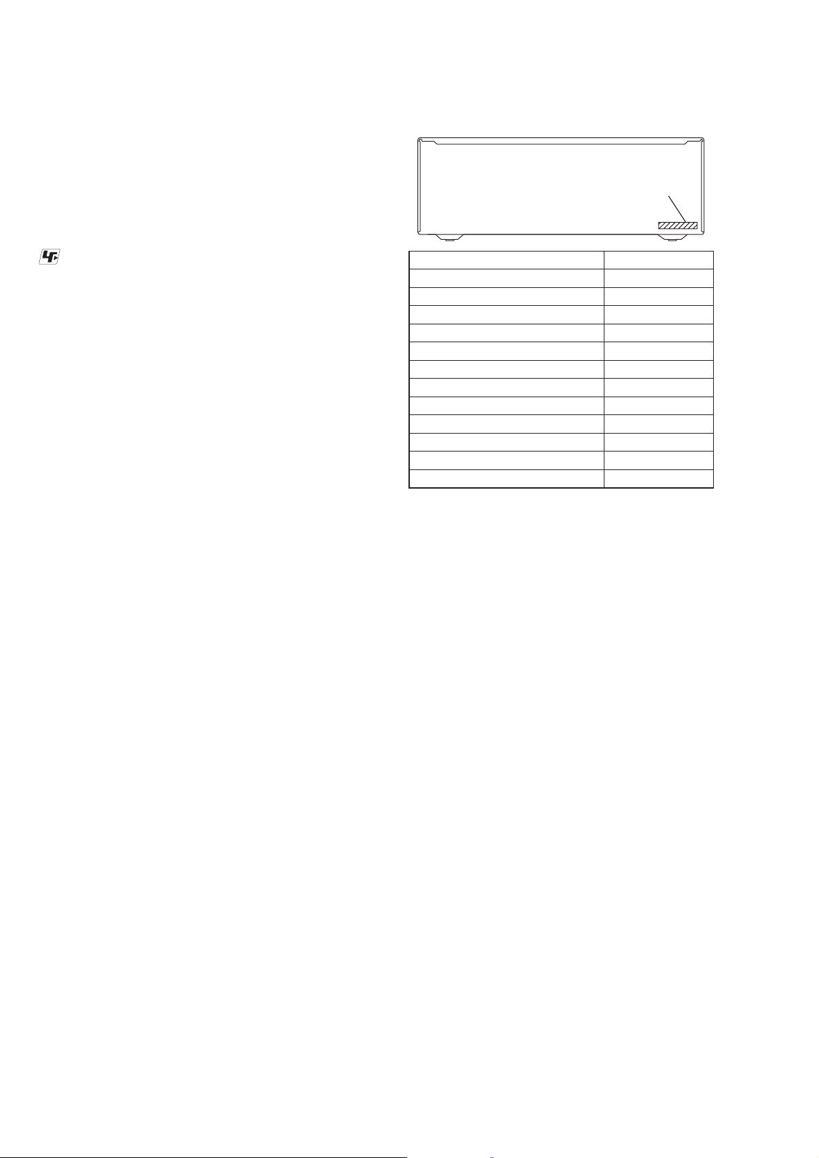
SAFETY-RELATED COMPONENT WARNING!
COMPONENTS IDENTIFIED BY MARK 0OR DOTTED LINE
WITH MARK 0ON THE SCHEMATIC DIAGRAMS AND IN
THE PARTS LIST ARE CRITICAL TO SAFE OPERATION.
REPLACE THESE COMPONENTS WITH SONY PARTS
WHOSE PART NUMBERS APPEAR AS SHOWN IN THIS
MANUAL OR IN SUPPLEMENTS PUBLISHED BY SONY.
1. SERVICING NOTES................................................. 4
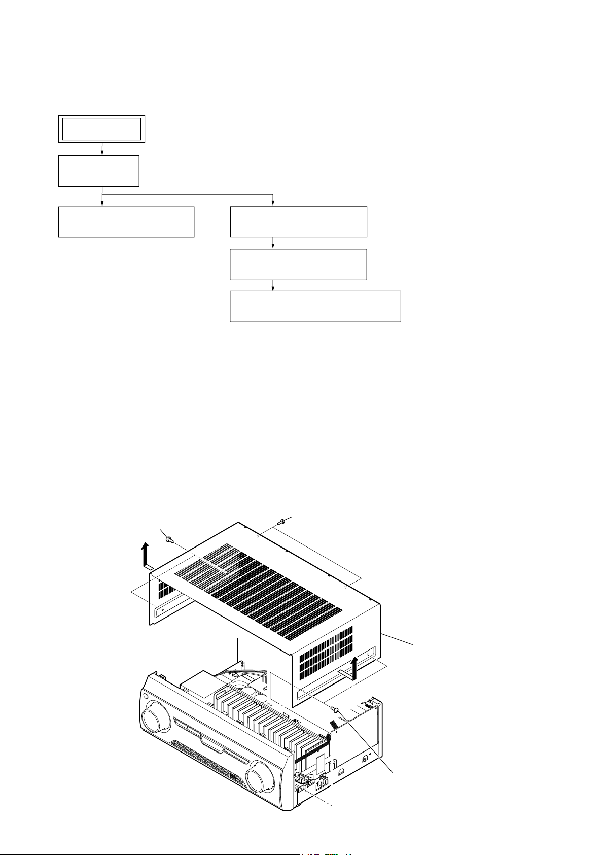
2. DISASSEMBLY
2-1. Disassembly Flow.............................................................. 6
2-2. Case.................................................................................... 6
2-3. Front Panel Section............................................................ 7
2-4. Back Panel Section ............................................................ 7
2-5. Main Block Section ........................................................... 8
2-6. MAIN Board, THERMAL Board...................................... 8
3. TEST MODE................................................................ 9
4. ELECTRICAL CHECK............................................11
5. DIAGRAMS
5-1. Block Diagram - TUNER/AUDIO Section -................... 13
5-2. Block Diagram - DIGITAL Section -............................... 14
5-3. Block Diagram - HDMI Section -.................................... 15
5-4. Block Diagram - KEY/DISPLAY/USB Section -............ 16
5-5. Block Diagram - POWER KEY Section -....................... 17
5-6. Printed Wiring Board
- DIGITALAUDIO Board (Side A) -.............................. 19
5-7. Printed Wiring Board
- DIGITALAUDIO Board (Side B) -.............................. 20
5-8. Schematic Diagram
- DIGITALAUDIO Board (1/4) -.................................... 21
5-9. Schematic Diagram
- DIGITALAUDIO Board (2/4) -.................................... 22
5-10. Schematic Diagram
- DIGITALAUDIO Board (3/4) -.................................... 23
5-11. Schematic Diagram
- DIGITALAUDIO Board (4/4) -.................................... 24
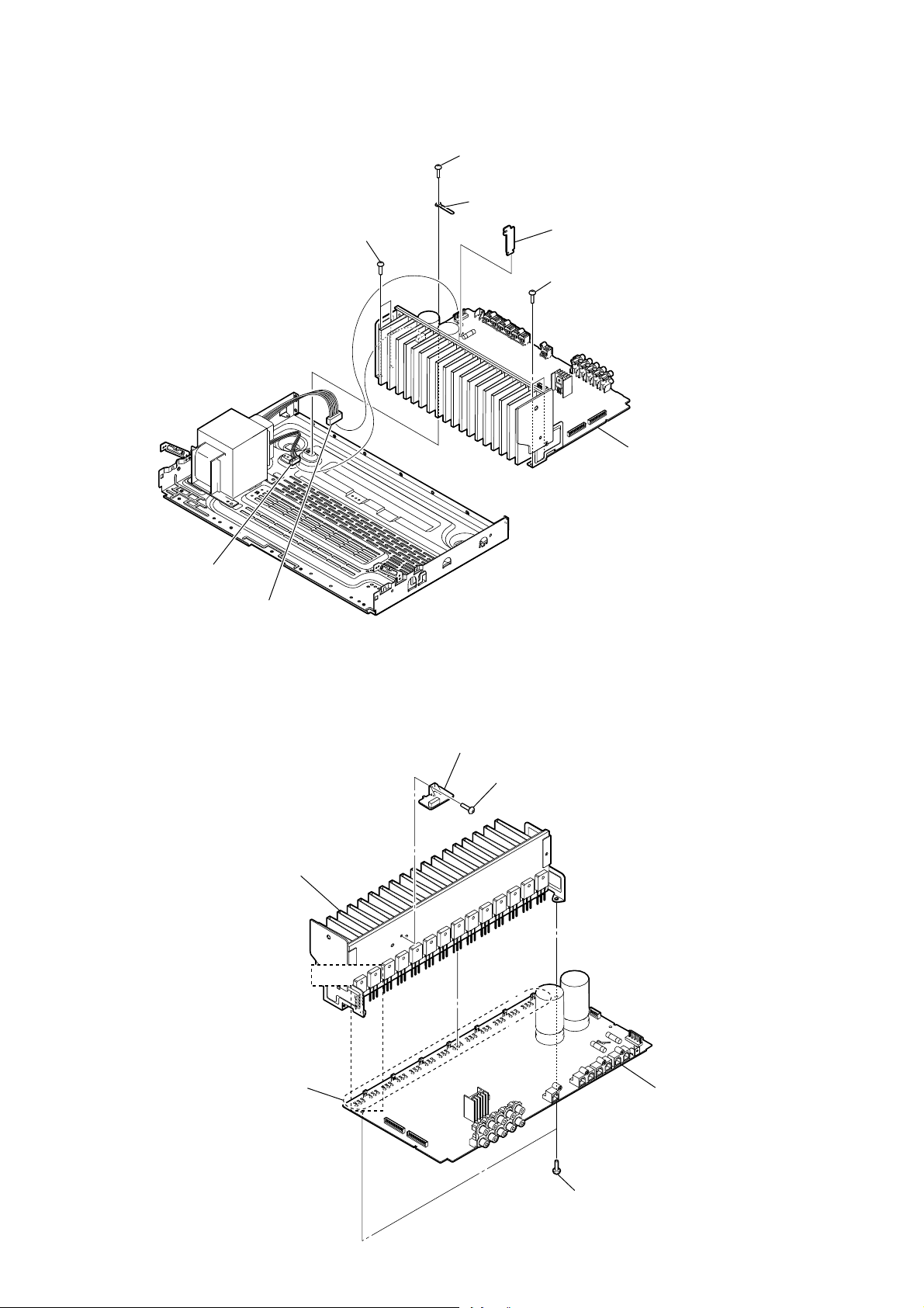
5-12. Printed Wiring Board - MAIN Board -............................ 25
5-13. Schematic Diagram - MAIN Board (1/4) -...................... 26
5-14. Schematic Diagram - MAIN Board (2/4) -...................... 27
5-15. Schematic Diagram - MAIN Board (3/4) -...................... 28
5-16. Schematic Diagram - MAIN Board (4/4) -...................... 29
TABLE OF CONTENTS
5-17. Printed Wiring Board
- HDMI RE Board (Side A) (KM3) -............................... 30
5-18. Printed Wiring Board
- HDMI RE Board (Side B) (KM3) - .............................. 31
5-19. Schematic Diagram
- HDMI RE Board (1/2) (KM3) - .................................... 32
5-20. Schematic Diagram
- HDMI RE Board (2/2) (KM3) - .................................... 33
5-21. Printed Wiring Board - POWER AVIDEO Board -......... 34
5-22. Schematic Diagram - POWER AVIDEO Board -............ 35
5-23. Printed Wiring Board - DISPLAY Board -...................... 36
5-24. Schematic Diagram - DISPLAY Board -......................... 37
5-25. Printed Wiring Board - DCDC Board - ........................... 38
5-26. Schematic Diagram - DCDC Board -.............................. 39
5-27. Printed Wiring Board - LED BAR Board -...................... 40
5-28. Schematic Diagram - LED BAR Board - ........................ 40
5-29. Printed Wiring Board
- USB Board (EXCEPT SAF, AR) -................................ 41
5-30. Schematic Diagram
- USB Board (EXCEPT SAF, AR) -................................ 42
5-31. Printed Wiring Board - TUNER1 Board - ....................... 43
5-32. Schematic Diagram - TUNER1 Board -.......................... 43
5-33. Printed Wiring Board - POWER KEY Board -................ 44
5-34. Schematic Diagram - POWER KEY Board -.................. 44
5-35. Printed Wiring Board - THERMAL Board - ................... 44
5-36. Schematic Diagram - THERMAL Board - ...................... 44
6. EXPLODED VIEWS
6-1. Case Section..................................................................... 58
6-2. Front Panel Section.......................................................... 59
6-3. Back Panel Section .......................................................... 60
6-4. Chassis Section ................................................................ 61
6-5. Heatsink Section .............................................................. 62
7. ELECTRICAL PARTS LIST................................ 63

STR-KM2/KM3
4
SECTION 1
SERVICING NOTES
Notes on chip component replacement
• Never reuse a disconnected chip component.
• Notice that the minus side of a tantalum capacitor may be da-
maged by heat.
UNLEADED SOLDER
Boards requiring use of unleaded solder are printed with the lead-
free mark (LF) indicating the solder contains no lead.
(Caution: Some printed circuit boards may not come printed with
the lead free mark due to their particular size)
: LEAD FREE MARK
Unleaded solder has the following characteristics.
• Unleaded solder melts at a temperature about 40 °C higher
than ordinary solder.
Ordinary soldering irons can be used but the iron tip has to be
applied to the solder joint for a slightly longer time.
Soldering irons using a temperature regulator should be set to
about 350 °C.
Caution: The printed pattern (copper foil) may peel away if the
heated tip is applied for too long, so be careful!
• Strong viscosity
Unleaded solder is more viscou-s (sticky, less prone to flow)
than ordinary solder so use caution not to let solder bridges
occur such as on IC pins, etc.
• Usable with ordinary solder
It is best to use only unleaded solder but unleaded solder may
also be added to ordinary solder.
Special Component Notice
The components identified by mark 9contain confidential
information.
Strictly follow the instructions whenever the components are
repaired and/or replaced.
NOTE OF REPLACING THE IC2036 AND IC2811 ON
THE DIGITAL AUDIO BOARD
IC2036 and IC2811 on the DIGITAL AUDIO board cannot
exchange with single. When these parts on the DIGITAL AUDIO
board are damaged, exchange the entire mounted board.
NOTE OF REPLACING THE IC3500 AND IC3501 ON
THE HDMI RE BOARD (KM3)
IC3500 and IC3501 on the HDMI RE board cannot exchange
with single. When these parts on the HDMI RE board are
damaged, exchange the entire mounted board.
MODEL IDENTIFICATION
- Rear View -
Part NO.
Model Part No.
KM3: SAF 4-409-905-0[]
KM3: TH 4-409-905-2[]
KM3: AUS 4-409-905-3[]
KM3: EA 4-409-905-4[]
KM3: E51 4-409-905-6[]
KM3: MX 4-409-905-7[]
KM3: AR 4-409-905-8[]
KM3: SP 4-409-905-9[]
KM2: SAF 4-409-906-0[]
KM2: E51 4-409-906-1[]
KM2: AR 4-409-906-2[]
KM3: RU 4-430-214-1[]
• Abbreviation
AR : Argentina model
AUS : Australian model
E51 : Chilean and Peruvian models
EA : Saudi Arabia model
MX : Mexican model
RU : Russian model
SAF : South African model
SP : Singapore model
TH : Thai model
Ver. 1.1

STR-KM2/KM3
5
MICOM (IC2105) ON DIGITAL AUDIO BOARD SERVICE POSITION
• In checking the MICOM (IC2105) on the DIGITAL AUDIO board, prepare a set of extension jigs (A-1870-129-A) which consists of
three extension cables and one RCA cord / audio cord (for grounding purpose).
HDMI RE board (KM3)
Extension jigs
(A-1870-129-A)
DCDC board
DIGITAL AUDIO board
THERMAL board
Connect jig to the HDMI RE board (CN3510 (5P)) (KM3),
DCDC board (CN1503 (13P)) and
DIGITAL AUDIO board (CN2502 (8P))
Connect jig to the POWER AVIDEO board (CN271 (12P)),
and DIGITAL AUDIO board (CN2103 (12P))
Connect jig to the MAIN board (CN300 (14P)), (CN301 (14P)) and
DIGITAL AUDIO board (CN2105 (14P)), (CN2104 (14P))
Connect RCA cord / audio cord to the
DIGITAL AUDIO board (J2301
(DIGITAL COAXIAL BD/DVD IN))
and MAIN board (J302
(VIDEO AUDIO OUT/IN))
MAIN board
POWER AVIDEO board
Ver. 1.1

STR-KM2/KM3
6
SECTION 2
DISASSEMBLY
• This set can be disassembled in the order shown below.
2-1. DISASSEMBLY FLOW
Note: Follow the disassembly procedure in the numerical order given.
2-2. CASE
3two screws
(+BVTP 3 u8)
4
4
2two screws
(+BVST 4 u8)
5case
1two screws
(+BVST 4 u8)
2-2. CASE
(Page 6)
2-3. FRONT PANEL SECTION
(Page 7) 2-4. BACK PANEL SECTION
(Page 7)
2-5. MAIN BLOCK SECTION
(Page 8)
2-6. MAIN BOARD, THERMAL BOARD
(Page 8)
SET

STR-KM2/KM3
7
2-3. FRONT PANEL SECTION
2-4. BACK PANEL SECTION
1CN2504 (13P)
3wire (flat type)
(15 core) (CN2503)
2saranet cushion
4one screw
(+BVTP 3 u8)
4one screw
(+BVTP 3 u8)
5one screw
(+BVTP 3 u8)
5one screw
(+BVTP 3 u8)
6five screws
(+BVTP 3 u8)
7one screw
(+BVTP 3 u8)
9front panel block
8claw
8claw
(except SAF, AR)
(except SAF, AR)
• Abbreviation
AR : Argentina model
SAF : South African model
1CN2501 (4P)
2CN911 (4P)
3CNP902 (4P)
4CNP903 (3P)
5five screws
(+BVTP 3 u8)
6six screws
(+BVTP 3 u8)
7one screw
(+BVTP 3 u8)
(KM3)
(KM3)
(KM2: E51)
(KM3: E51, EA, MX)
0back panel block
9CN2104 (14P)
8CN2105 (14P)
• Abbreviation
E51 : Chilean and Peruvian models
EA : Saudi Arabia model
MX : Mexican model

STR-KM2/KM3
8
2-5. MAIN BLOCK SECTION
2-6. MAIN BOARD, THERMAL BOARD
4one screw
(+BVTP 3 u8)
6two screws
(+BVTP 3 u8) 1LOCK board
8MAIN block
2CN951
(5P)
3CN950
(5P)
7two screws
(+BVTP 3 u8)
5clamp
6heatsink block
4two screws
(+BVTP 3 u8)
5MAIN board
3Remove the thirty-six solders.
(KM2)
Remove the forty-two solders.
(KM3)
1one screw
(+BVTP 3 u8)
2THERMAL board
(KM3)

STR-KM2/KM3
9
SECTION 3
TEST MODE
FL CHECK MODE
All fluorescent segments are tested. When this test is activated, all
segments turn on at the same time, then each segment turns on one
after another.
Procedure:
1.
When pressing the [SURROUND SPEAKER] and [M-TURBO]
buttons, press the [?/1] button to turn on the main power.
2. All segments turn on.
L C R
SL S SR
SBL SB SBR
LH RH SW COAX OPT
HDMILFE DTS -ES NEO:6 USB
96/24
DTS-HD MSTR HI RES LBR LPCM
RDS
AAC
TrueHD
SLEEP
D.RANGE
ST
D
PL II
+ EX
MHz
ft.
k Hz m
x z
dB
3. Turn the [INPUT SELECTOR] dial.
4. Test pattern 1 turn on.
LCR
SL SSR
SBL SB SBR
LH RH SW COAX OPT
HDMILFE DTS -ES NEO:6 S-AIR
96/24
DTS-HD MSTR HI RES LBR LPCM AAC
TrueHD
SLEEP
D.RANGE
PL+
ft.
k m
z
dB
5. Turn the [INPUT SELECTOR] dial once again.
6. Test pattern 2 turn on.
L R
S
SBL SBR
LH RH SW COAX OPT
HDMILFE DTS -ES NEO:6 USB
96/24
DTS-HD MSTR HI RES LBR LPCM
RDS
TrueHD
SLEEP
D.RANGE
ST
D
PL IIEX
MHz
Hz
x
7. Turn the [INPUT SELECTOR] dial once again. All segments
turn off.
8. Every turning of the [INPUT SELECTOR] dial turns on each
segment one after another on the same order.
S.F. CLEAR MODE
The preset sound filed is cleared when this mode is activated. Use
this mode before returning the product to clients upon completion
of repair.
Procedure:
1. While pressing the [MUSIC] button, press the [?/1] button to
turn on the main power.
2. The message “S.F. CLEAR” appears and initialization is per-
formed.
USER INITIALIZE MODE
All preset contents are cleared when this mode is activated. Use
this mode before returning the product to clients upon completion
of repair.
Procedure:
1. Hold the [?/1] for 5 seconds.
2. The message “CLEARING” appears on the display.
3. After a few seconds, “CLEARED” appears.
SOFTWARE VERSION DISPLAY MODE
The software version is displayed.
Procedure:
1. While pressing the [SURROUND SPEAKER] and [MUSIC]
buttons, press the [?/1] button to turn on the main power.
2.
The message “M2**Mx.xx” appears. This is main micropro-
cessor version (KM2).
The message “M3**Mx.xx” appears. This is main micropro-
cessor version (KM3).
**: destination, x.xx: software version
3. Press the [DISPLAY] button on the remote commander,
DSP firmware version
“S. VER x.xx” appears.
Sound tuning version
“M2 ST x.xx” appears (KM2).
“M3 ST x.xx” appears (KM3).
Tuner Version
“T.VER x.xx” appears.
SPDIF UPDATE MODE
User plays the CD that contains u-com/DSP data with CD/DVD
player.
Update u-com/DSP etc. firmware from SPDIF input.
Connection:
CD/DVD
player
DIGITAL board
COAXIAL BD/DVD IN jack (J2301)
set
Procedure:
Normal case
1. While pressing [MOVIE] and [M-TURBO] buttons, press the
[?/1] button to turn on the main power.
2. The messages “UPDATE” and “PLAY.DISC” are displayed
alternately every one second.
After this step, all user operation is prohibited except power
off. To cancel this mode, power off or AC power cord pull out
is required.
3. Connect CD player to COAXIAL BD/DVD IN jack (J2301 on
the DIGITAL board), and play update CD.
Update is started when DSP detect update signal. The message
“UPDATING” is displayed blinks every one second.
From this step, all user operation is prohibited. Power off is
also prohibited.
4. While main u-com is being updated, fluorescent indicator tube
is blacked out.
5. When update data error is detected or disc is not matched with
target model, error messages “DISC ERR” and “PLAY.DISC”
are displayed to restart playing valid CD.
When flash writing error is happened, error messages
“UPT. ERR” and “PLAY.DISC” are displayed to restart play-
ing CD.
6. When all update is finished, set is reboot automatically. After
reboot, complete message “COMPLETE” is displayed (dis-
played continuously until any user operation).

STR-KM2/KM3
10
Procedure:
After update is abnormal exit, and set is power on again
1. Enter update mode automatically after power on.
2. The messages “UPDATE” and “PLAY.DISC” are displayed
alternately every one second.
From this step, all user operation is prohibited. Power off is
also prohibited.
If main u-com was failed to update, nothing is displayed.
3. Connect CD player to COAXIAL BD/DVD IN jack (J2301 on
the DIGITAL board), and play update CD.
Update is started when DSP detect update signal. From this,
same as normal case.
SPDIF UPDATE VERSION MODE
Function that displays the version number to check whether SPDIF
update is necessary or not.
Procedure:
1. While pressing [MOVIE] and [MUSIC] buttons, press the
[?/1] button to turn on the main power.
2. The message “VER X.XXX” is displayed. “X.XXX” is calcu-
lated by adding all firmware version.
Example:
(MAIN ver. + DSP ver. + SOUND TUNE ver. + 7)/10 =
Displayed version
MAIN = 1.02, DSP = 1.01, SOUND TUNE = 1.00
↓
(1.02 + 1.01 + 1.00 + 7)/10 = 1.003
1.003 = X.XXX
HISTORY MODE
The state that the set is used is memorized.
Procedure:
1. While depressing the [SURROUND SPEAKER] and the
[GAMING] buttons simultaneously, press the [?/1] button to
turn on the main power.
2. “HISTORY” appears.
3. Each time the [V] / [v] buttons on the remote control is pressed,
the item is switched in order as follows.
Items Display
Protector Count COUNT xx
Total Single Power On Time xxxxxHxx 01
Surround Speaker Position SURPOS X
Sound Field SND FLD
Input Function FUNCTION
Input Mode INP MODE
Digital Select DIG IN
Stream Information STREAM
Signal Configuration CO xxxxx
Headphone HP xxx
Volume VOL xx
Bass BASS xxx
Treble TREB xxx
Level FL/FR F xxxxxx
Level SL/SR S xxxxxx
Level CT/SW CWxxxxxx
Level BL/BR B xxxxxx
Total Power ON Time xxxxxHxx 02
Muting MUTE xxx
Power ON Counter (Rebox Test Mode) REBXxxxx
Protector Type PROTxxxx
Temperature Record TEM xxxx
VACS Step VACS xx
PROTECTOR ON/OFF
*To disable auto off after protector occur.
Procedure:
1. While depressing the [MOVIE] and the [GAMING] buttons
simultaneously, press the power [?/1] button to turn on the
main power.
2. “PROTEVER” appears.

STR-KM2/KM3
11
SECTION 4
ELECTRICAL CHECK
FM AUTO STOP CHECK
signal
generator set
Procedure:
1. Turn on the set.
2. Input the following signal from signal generator to FM antenna
input directly.
Carrier frequency: A = 87.5 MHz, B = 98 MHz, C = 108 MHz
Deviation : 75 kHz
Modulation : 1 kHz
Note: Use 75 ohm coaxial cable to connect signal generator and the set.
You cannot use video cable for checking.
Use signal generator whose output impedance is 75 ohm.
3. Set to FM tuner function and scan the input FM signal with
automatic scanning.
4. Confirm that input frequency of A, B and C are detected and
automatic scanning stops.
When the station signal is received in good condition, automatic
scanning stops.

STR-KM2/KM3
12
• Abbreviation
AR : Argentina model
SAF : South African model
SECTION 5
DIAGRAMS
• Circuit Boards Location
POWER KEY board
LED BAR board
DISPLAY board
POWER AVIDEO board
DCDC board
TUNER1 board
HDMI RE board
(KM3)
DIGITAL AUDIO board
MAIN board
THERMAL board
USB board
(except SAF, AR)

5-1. BLOCK DIAGRAM – TUNER/AUDIO Section –
C-CH
SR-CH
FR-CH
SL-CH
FL-CH
R-IN
L-IN
SW
SEL
C
SEL
SL
SEL
R-CH
INR2
INL2
ROUT
LOUT
R-CH
R-CH
DIR
FUNCTION SELECT
IC300
VCCVEE
+7V
SEL
SW
MCU
I/F
-7V
SW OUT
C OUT
SLOUT
FLOUT
SYSTEM
CONTROL
IC2105 (1/4)
FM RECEIVER
IC101
CN104
CN103
EVOL_DATA
EVOL_CLK 98
97
12 8
10
62
11
75
14
13
18
17
SW-CH
16
71 70 68 69
SR OUT
FR OUT
72 73
54
53
50
49
58
57
46
45
15
76
25
26
L
SEL
14
6115
FRF1
ARF1
4
6
ARF2
7
X101
32.768kHz
19 18
X2
X1
+3.3V
+5V
+3.3V
REG 43
IC102
J302(1/2) J300
-1 -2 -4 -5
-4 -5 J302 (2/2)
-1 -2
SA-CD/CD
AUDIO IN
L R
TV
AUDIO IN
L R
-7 -8
PORTABLE
AUDIO IN
L R
L R
VIDEO
AUDIO IN
L R
VIDEO
AUDIO OUT
FM
AM
AM
&2$;,$/
FM
AM
ANTENNA
6LJQDOSDWK
: TUNER (FM/AM)
: TUNER
5FKLVRPLWWHGGXHWR
VDPHDV/FK
DIGITAL
SECTION
(Page 14)
DIGITAL
SECTION
(Page 14)
POWER KEY
SECTION
(Page 17)
A
B
C
MX
STR-KM2/KM3
STR-KM2/KM3
1313

5-2. BLOCK DIAGRAM – DIGITAL Section –
TUNER/
AUDIO
SECTION
(Page 13)
C
TUNER/
AUDIO
SECTION
(Page 13) A
HDMI
SECTION
(Page 15) D
L-IN
R-IN
3 - 5
14 - 16
19 - 21
75, 97,103
6 - 9
74, 95,101
6LJQDO SDWK
: TUNER (FM/AM)
: DVD (DIGITAL)
R-FK LV RPLWWHG GXH WR
VDPH DV L-FK
COAXIAL
BD/DVD IN
DIGITAL
OPTICAL
6AT/CATV
IN
J2301
OPTICAL
GAME IN X2800
25MHz
CN2508
12
13
16
11
14
7
9
10
21
18
15
44 13
45
73
94
86
X2801
24576MHz
CLKIN
6L/6RBOUT
C/6:1BOUT
L/RBOUT
24
XTAL2
25
92
BCLKBOUT
MCLKBIN 98
LRCLKBOUT
6PICLK
Y0
B0 Y3
Y1
6EL
MO6I
MI6O
IRQ/GPIO
FLAG1
FLAG2
99
70 71 68
31
32
88 89
37 38
INPUT DATA
DEMODULATOR
PD,PEDETECTION LOCK
DETECTION
MICROPROCE66OR
I/F
C ELW DETECTION
15
1
OUT
1
8
96
CKA
Q4B
DIGITAL OPTICAL
RECEIVE
IC2352
DIGITALAUDIO
INTERFACE RECEIVER
IC2806 (1/2)
23
:AVE 6HAPER
IC2303
IC2010
81
18
33V
REG
12V VDDI
33VVDDE
33V
TEMPB6EN6ORB1
VDD
33V
11V REG
IC2813
11V +4V
VOUT VIN
D6P
IC2801 (1/2)
COMBCLK
57
HDMIB6CL
COMBDATA
6CK COMBCLK
6I COMBDATA
63
58
TH251
6ELECTOR
IC3527
28
+33V
RE6ET 6IGNALGENERATOR
IC2034
12
+33V
D2722
D2723
TH252
26
TEMPB6EN6ORB2
27
XOUT
RXIN1
COAXIAL
RXIN6
OPTICAL6AT/ CATV
D6P LRCKLRCKOUT
1
OUT
IN2 OUT3
DIGITAL OPTICAL
RECEIVE
IC2351
59
RXIN5
OPTICALGAME
XIN
6Y6TEM
CONTROL
IC2105 (2/4)
1114
94
18
19
20
652
95
MUTE
LAT
MUTE
M/LAT
12
MC/CLK
13
MD/DATA
DIN3 FLOUT
R-CH
VO3L
VO3R
VO2L
VO2R
VO1L
VO1R
9
26
25
7
2MCK
3BCK
LRCK
4
D/ACONVERTER
IC2123
DIN2 C OUT
R-CH
23
DAC
DAC
DIN1 6L OUT
21
6: OUT
22
DAC
DAC
D6P
69
RXIN3 HDMI 6PDIF
ADINR
ADINL
D6P MCK MCKOUT
CEC 6:ITCH
IC2811
134
135
136
3
10 8
6
4
1
2
8
2
5
1
6CHMITTRIGGER
IC2009
6IGNAL
6ELECTOR
IC2032 (1/2)
EEPROM
IC2802
CN2506
4
5
6
FLA6H
PROGRAMMING
CN2509
4
5
6
FLA6H
PROGRAMMING
12
4
7
1
3
3Y
9
3A
11
CECBIN
CEC CECBOUT 2
1
4
MUTING
IC2804
BINARY
COUNTER
IC2007
3
3
61
RXIN4ARC 6PDIF
60
4746
HDMIBCECIN
HDMIBCECOUT
D6PBMI6O
D6PBMO6I
D6PB6PICLK
6EL
NPCM
ERROR
INT
F6RATE
60
6O
61
FLA6HBCLK
62
UARTB6EL
59
6I
38
39
40
UARTBOUT 49
UARTBIN 50
6CK
6I
6O
173
RE6ET Y0
Y1
Y2
A2
A1
A0
B0
CK
D
Q
6IGNAL6ELECTOR
IC2805
MUTE
6:ITCH
Q2706
1
6ELECT
24
KM3
STR-KM2/KM3
STR-KM2/KM3
1414

5-3. BLOCK DIAGRAM – HDMI Section –
125 R1X2+
DATA2+
DATA2–
DATA1+
DATA1–
DATA0+
DATA0–
CLOCK+
CLOCK–
SCL(5V)
SDA(5V)
HOT PLUG DET
CEC
+5V POWER
DATA2+
DATA2–
DATA1+
DATA1–
DATA0+
DATA0–
CLOCK+
CLOCK–
SCL(5V)
SDA(5V)
HOT PLUG DET
CEC
+5V POWER
DATA2+
DATA2–
DATA1+
DATA1–
DATA0+
DATA0–
CLOCK+
CLOCK–
SCL(5V)
SDA(5V)
HOT PLUG DET
CEC
+5V POWER
R1X2-
R1X1+
R1X1-
Q0
I
Q35
D0
I
D35
R1X0+
R1X0-
R1XC+
R1XC-
DSCL1
124
123
122
121
120
119
118
35
134 R2X2+
R2X2-
R2X1+
R2X1-
R2X0+
R2X0-
R2XC+
R2XC-
133
132
131
130
129
128
127 DSCL2
DSDA2
39
40 HPD2
R3X2+
R3X2-
R3X1+
R3X1-
R3X0+
R3X0-
R3XC+
R3XC-
DSCL3
DSDA3
HPD3
38
TX2+
TX2-
TX1+
TX1-
TX0+
TX0-
TXC+
TXC-
DSCL
DSDA
HPD
40
39
37
36
34
33
31
30
46
47
51
DSDA1
HPD1
36
34
DE
73
VSYNC 74
73
HSYNC 75
SCK/DCLK 100
WS/DR0 99
SD0/DL0 101
SD1/DR1 102
SD2/DL1 103
SD3/DR2 104
SPDIF/DL2 106
1
DE
VSYNC
HSYNC
DL2
48 CSCL
CSDA
49
21
MCLK
5
DR2
20
DL1
19
DR1
18
DL0
17
DCLK
15
DR0
16
R1PWR5V33
R2PWER5V37
R3PWR5V41
IC3500
HDMI RECEIVER
IC3501
HDMI TRANSMITTER (1/2)
23
24
IC3501
HDMI TRANSMITTER
(2/2)
CSDA
CSCL
DATA2+
DATA2–
DATA1+
DATA1–
DATA0+
DATA0–
CLOCK+
CLOCK–
SCL(5V)
SDA(5V)
HOT PLUG DET
CEC
+5V POWER
8 2
+4V REG
IC1500
1 8
+1.83V
REG
IC3530
+1.8V
1 6
+3.3V
REG
IC3532
+3.3V
+5V
+13V
143
142
141
140
139
138
137
136
43
44
42
96-88,
85-77,
70-62,
59-51
98-90,
86-77,
75-67,
63-56
4
5
XTALOUT
XTALIN X3501
27MHz
1
4
5
IC3533
+5V REG
2
8
IC1600
+6 REG
+5V
+13V
+5V
5
4
IC3509
+5V REG
CN3512
DIGITAL
SECTION
(Page 14)
7
8
9
10
11
12
13
15
1
18
A6
7
A7
8
A2
3
A3
4
A4
5
A5
6
A8
9
A1
Y1
Y8
2
IC3507
BUFFER
18
17
16
15
14
13
12
11
3
1
2
DCCPWR5V
45
D3529
1 8
+1.2V
REG
IC3531
+1.2V D3515
CN3503
4
6
1
3
7
9
10
12
15
16
19
13
18
CN3502
4
6
1
3
7
9
10
12
15
16
19
13
18
CN3500
4
6
1
3
7
9
10
12
15
16
19
13
18
TV OUT
ARC
CN3501
4
6
1
3
7
9
10
12
15
16
19
13
18
HDMI
SAT/CATV
IN
GAME
IN
BD/DVD
IN
WS
10
SCK
11
SD0
9
SD1
8
SD2
7
SD3
6
SPDIF
4
SLJQDO SDWK
: DVD (DIGITAL)
: VIDEO
D
KM3
STR-KM2/KM3
STR-KM2/KM3
1515

5-4. BLOCK DIAGRAM – KEY/DISPLAY/USB Section –
92
FL DISPLAY DRIVER
IC100
14
I
29
31
93
99
100
5
6
30
12
11
51
53
54
X1(X_OUT)
X0(X_IN)
E2P_SDA
E2P_SCL
POWER_KEY
MD2
MD0
RST
SDA
SCL
EEPROM
IC2106
SIRCS
22
FL_DATA 7DIN
21
FL_LAT 9STB
23
FL_CLK 8CLK
GRID1
I
GRID11
SEG1
I
SEG17
VOL_JOG
INPUT_JOG
AD_KEY_2
AD_KEY_1
31
2REMOTE
CONTROL
SIGNAL
RECEIVER
IC102
OUT
SIRCS
+6.3V DCDC
SYSTEM
CONTROL
IC2105 (3/4)
MD2
MD0
RESET
61
60 FLASH_CLK
SO
59 SI
CLK
SO
SI
41
2
34
36
RESET SWITCH
IC2019
DSP
IC2801 (2/2)
42
I
32
30
VEE
1
SW1
2
SW2
3
SW3
OUTIN
IN
Q2006
1
37
VOUT
USB_OVC
EXCEPT SAF, AR
REGISTOR CONTROL
IC4102
62
RXIN2 USB SPDIF
DIGITALAUDIO
INTERFACE RECEIVER
IC2806 (2/2)
64 Vout
1
Vin
FAULT
USB POWER SWITCH
IC4101
1
2
OUT
VDD RESET SIGNAL
GENERATOR
IC2020
41 OUT_YGate
2In
MAIN RESET SWITCH
IC2033
DATAPROCESSOR
IC4100
44
MD
47
RESET_MAIN
SPDIF
33
USB-DM 34
40
53
41
USB-DP
XIN-PLL
IRPTO,
KEY-ROW1/MCHNG,
KEY-ROW3/SCL,
KEY-ROW4/SDA
USB_IPOD_REQ,
USB_MCHNG,
USB_SDA,
USB_SCL
XOUT-PLL
13,12,10,8
39,48 - 50
IC4161
+3.3V
REG
+3.3V
+3.3V
STBY
+6.3V
DCDC
IC101
+3.3V
REG
+3.3V
CN4101
4
X2101
4MHz
X4102
16.9344MHz
CN2509
8
9
3
4
5
6
S100
_/1
SW NETWORK
S103-105
SW NETWORK
S101-102
T100
DC CONVERTER
TRANSFORMER
Q100
SWITCHING
TRANSISTOR
D120
D121
RV101
MASTER
VOLUME
2
3
RV100
INPUT
SELECTOR
2
3
ND100
VACUUM
FLUORESCENT
DISPLAY
D122
D123
SWITCHING
DIODE
INPUT LED
Q101 D100, D102 - D103,
D105, D107, D109
VOLUME LED
Q102 D139, D141 - D142,
D144, D146 - D147
BAR LED
Q103 D130, D132 - D133,
D135, D136, D138
FLASH
PROGRAMMING
D2019
3
4
2
D-
Vbus
D+
DATA
SWITCH
VD4170-
VD4171
D4107
E
ET4100
$EEUHYLDWLRQ
SAF : 6RXWK$IULFDQPRGHO
AR :$UJHQWLQDPRGHO
STR-KM2/KM3
STR-KM2/KM3
1616

5-5. BLOCK DIAGRAM – POWER KEY Section –
62
3
DRIVE
PRE DRIVER
IC701
IN 1 +VOUT1
-VOUT2
812
11
IN 2 +VOUT2
-VOUT2
FL-CH
FR-CH
FL-CH
FR-CH
SL-CH
SW-CH
SR-CH
SL-CH
SR-CH
+3.3V
(STBY)
-7V
+7V
1
62
3
DRIVE
PRE DRIVER
IC601
IN 1 +VOUT1
-VOUT2
812
11
IN 2 +VOUT2
-VOUT2
+5V
(STBY)
+3.3V
REG
IC2107
-15V
+15V
+7V
REG
IC951
+5V
REG
IC2812
-7V
REG
IC950
+5V
FRONT_SPK_A_RY
SBL-SBR_RY
C/SL-SR_RY
PROTECTOR
IO_EX_CLK
IO_EX_LAT
IO_EX_DATA
IO_EX_OE
FUSE_DET 82
SYSTEM
CONTROL
IC2105 (4/4)
PRE
DRIVE
C-CH 62
3
DRIVE
PRE DRIVER
IC501
IN 1 +VOUT1
-VOUT2
PRE
DRIVE
PRE
DRIVE
62
3
DRIVE
PRE DRIVER
IC801
IN 1 +VOUT1
-VOUT2
812
11
IN 2 +VOUT2
-VOUT2
PRE
DRIVE
VOLTAGE
DETECTION
IC2421
2-4,15
11-14
10-8,3
SHIFT REGISTER
IC2036
R
L
L
CENTER
SURROUND
SUBWOOFER
R
TB355
TB353
TB354
FRONT
SPEAKERS
T901
POWER TRANSFORMER
(MAIN)
F901
F902
POWER TRANSFORMER
(SUB)
T902
AC IN ~
RECT
D952
F952
F953
F954
F955
RY901
D904
F950
F951
F911
F912
RECT
D953-956
RECT
D912
PROTECTOR
D862-863
Q863-867
D520 -
523
POWERAMP
Q700-703,
Q750-753
POWERAMP
Q500-503,
Q550-553
POWERAMP
Q600-603,
Q650-653
POWERAMP
Q800-803
RY353
RY354
RELAY
DRIVER
Q354
RELAY
DRIVER
Q353
RY950
RELAY
DRIVER
Q950
D2110,
2302,
2303
RY355
RELAY
DRIVER
Q355
2
1
TB352
RY352
RELAY
DRIVER
Q352
CURRENT
DETECT
Q761,762
CURRENT
DETECT
Q711,712
CURRENT
DETECT
Q811,812
CURRENT
DETECT
Q561,562
CURRENT
DETECT
Q511,512
CURRENT
DETECT
Q661,662
CURRENT
DETECT
Q611,612
RELAY
DRIVER
Q901
AC IN
DETECT
Q902
RECT
D902,D903
240V
220V
120V
R
R
S901
VOLTAGE SELECTOR
SLJQDO SDWK
: TUNER (FM/AM)
R-FK LV RPLWWHG GXH WR
VDPH DV L-FK.
4
4
73
1
5 4
5 4
4 2
POWER_RY
80
STOP
TUNER/
AUDIO
SECTION
(Page 13)
B
SIGNAL
SELECTOR
IC2032 (2/2)
KM2: E51
KM3: E51, EA
KM2: E51
KM3: E51, EA, MX
EXCEPT MX
KM3
AEEUHYLDWLRQ
E51 : CKLOHDQ DQG PHUXYLDQ PRGHOV
EA : SDXGL AUDELD PRGHO
MX : MH[LFDQ PRGHO
STR-KM2/KM3
STR-KM2/KM3
1717

For Schematic Diagrams.
Note:
• All capacitors are in μF unless otherwise noted. (p: pF)
50 WV or less are not indicated except for electrolytics
and tantalums.
• All resistors are in and 1/4W or less unless otherwise
specified.
• f: internal component.
• 2: nonflammable resistor.
• 5: flusible resistor.
• C: panel designation.
THIS NOTE IS COMMON FOR PRINTED WIRING BOARDS AND SCHEMATIC DIAGRAMS.
(In addition to this, the necessary note is printed in each block.)
• A: B+ Line.
• B: B– Line.
• Voltages and waveforms are dc with respect to ground
under no-signal (detuned) conditions.
no mark : TUNER
• Voltages are taken with a VOM (Input impedance 10
M). Voltage variations may be noted due to normal pro-
duction tolerances.
• Waveforms are taken with a oscilloscope.
Voltage variations may be noted due to normal produc-
tion tolerances.
• Circled numbers refer to waveforms.
• Signal path.
F: TUNER (FM/AM)
f: TUNER
E: VIDEO
J: DVD (DIGITAL)
For Printed Wiring Boards.
Note:
• X: Parts extracted from the component side.
• Y: Parts extracted from the conductor side.
• f: Internal component.
• : Pattern from the side which enables seeing.
(The other layers' patterns are not indicated.)
• Indication of transistor.
C
BThese are omitted.
E
Q
CEBThese are omitted.
Note: The components identified by mark 0or dotted
line with mark 0are critical for safety.
Replace only with part number specified.
Caution:
Pattern face side:
(SIDE B)
Parts face side:
(SIDE A)
Parts on the pattern face side seen
from the pattern face are indicated.
Parts on the parts face side seen from
the parts face are indicated.
• Abbreviation
AR : Argentina model
AUS : Australian model
E51 : Chilean and Peruvian models
EA : Saudi Arabia model
MX : Mexican model
RU : Russian model
SAF : South African model
SP : Singapore model
TH : Thai model
• Abbreviation
AR : Argentina model
AUS : Australian model
E51 : Chilean and Peruvian models
EA : Saudi Arabia model
MX : Mexican model
RU : Russian model
SAF : South African model
SP : Singapore model
TH : Thai model
240m Vp-p
24.59 MHz
2IC2123 2(MCK)
100 mV/DIV, 10 ns/DIV
1.54 Vp-p
24.57 MHz
5IC2806 ea (XOUT)
500 mV/DIV, 10 ns/DIV
3.0 Vp-p
4.0 MHz
1IC2105 os (X1(X_OUT))
500 mV/DIV, 100 ns/DIV
3.0 Vp-p
3.1 MHz
3IC2123 3(BCK)
500 mV/DIV, 100 ns/DIV
3.4 Vp-p
47.81 kHz
4IC2123 4(LRCK)
500 mV/DIV, 5 Ps/DIV
• Waveforms
– DIGITAL AUDIO Board – – DISPLAY Board –
6IC100 5(OSC)
200 mV/DIV, 2.5 Ps/DIV
154.8 kHz 1.29 Vp-p
Ver. 1.1
STR-KM2/KM3
STR-KM2/KM3
1818

STR-KM2/KM3
STR-KM2/KM3
1919
5-6. PRINTED WIRING BOARD – DIGITAL AUDIO Board (Side A) – • See page 12 for Circuit Boards Location. • : Uses unleaded solder.
1
A
B
C
D
E
F
G
H
I
J
K
2 3 4 5 6 7 8 9 10 11 12 13 14 15 16
IC2106
IC2812
1100 8180
51
30
31
IC2105
50
IC2804
IC2036
IC2421
IC2007 IC2805
IC2123
IC2009
114
1528
IC2351 IC2352
IC2806
116
17
32
3348
49
64
IC2303
IC2813
133
132 88
89
45
44
1761
IC2801
177
IC2019
IC2033
IC2020
IC2802
IC2010
VCC O VCC O
R2860
R2861
R2863
R2864
R2865
R2866
R2867
R2868
R2099
R2872
R2875
R2876
RB2010
R2880
R2881
R2882
R2886
R2889
R2895
R2897
R2898
R2899
112
CN2103
CN2104
CN2105 111414
C2101
1
113
4
CN2501
18
CN2502
1215
14
CN2503
CN2504
16
CN2506
1221
20
CN2508
C2114
CN2509
19
C2501
C2119
C2502
C2503
C2504
C2507
C2121
C2125
C2126
C2127
R2100
C2128
C2512
R2105
R2107
X2800
C2130
R2109
X2801
C2901
C2131
D2302
D2303
D2110
C2136
C2137
C2909
R2111
R2112
R2116 C2140
C2912
C2913
FB2603 FB2604
R2311
C2917
FB2608
C2918
R2124
R2125
FB2031
FB2032 C2920
R2129
C2923
R2321 R2322
R2132
R2327
C2351
R2906
FB2043
D2717
C2354
D2719
C2355
C2358
C2359
D2720
D2721
D2722
R2912
D2723
D2724
C2361
R2725
R2919
R2726
R2727
R2728
R2729
C2370
R2925
R2732
R2733
R2540
R2158
R2735
R2541
R2159
R2929
R2736
R2351 R2354
R2930
R2932
R2356
R2933
R2357
R2358
C2961
C2962
C2963
C2964
C2965
C2966
C2967
R2940
C2968
R2941
C2969
R2172
R2173
R2945
R2947
R2948
C2970
R2949
C2972
C2973
C2974
C2975
R2759
C2976
C2977
C2978
R2957 R2958
R2959
R2960
R2962
R2963
RB2102
R2392
RB2103
RB2104
RB2105
RB2107
RB2109
FB2884
R2979
FB2885
FB2889
R2983
R2984
FB2890
R2985
FB2891
RB2119
R2986
FB2892
R2987
FB2893
FB2894
R2989
RB2121
RB2123
RB2124
RB2125
RB2126
R2992
RB2127
R2993
R2997
R2998
R2999
C2001
JL2808
JL2809
X2101
JL2811
JL2812
C2203
C2011
C2206
C2013
J2301
C2402
C2022
C2023
FB2101
C2413
C2609
R2006
R2007 C2418
C2421
C2422
D2018
C2424
R2015
C2619
FB2501
FB2502
C2814
R2211
C2815
C2816 C2818
R2601
R2602
R2607
C2823
C2248
R2220
C2825
C2826
R2802
R2610
R2809
R2615
R2421
R2617
R2618
R2619
C2838
C2069
R2815
R2621
R2622
R2816
C2070
C2841
C2459
R2626
C2842
C2266
C2072
C2074
C2846
C2847
C2849
R2052
R2824
R2825
R2249
C2465
R2826
C2466
C2273
R2058
C2274
C2468
R2829
R2059
C2469
C2858
C2470
R2831
R2834
R2835
R2837
R2838
C2860
C2861
C2863
C2864
C2865
C2866
C2096
C2868 C2869
R2843
R2846
R2847
R2849
C2873
C2875
C2876
C2877
R2851
R2852
R2854
R2855
R2856
R2857
R2858
R2859
C2881
C2883
R2002
FB2896
FB2801
291 8
CN2505
FB2033
FB2898
FB2899
R2620
A2001
R2157
C2853
DIGITAL
AUDIO
BOARD
(SIDE A)
1-885-324- 11
(11)
(CHASSIS)
(CHASSIS)
COAXIAL
BD/DVD IN
FLASH
PROGRAMMING
OPTICAL
SAT/
CATV
IN
OPTICAL
GAME
IN
DIGITAL
I
MAIN BOARD
CN300
(Page 25) H
MAIN BOARD
CN301
(Page 25)
A
TUNER1
BOARD
CN101
(Page 43)
B
LED BAR
BOARD
CN104
(Page 40)
C
THERMAL
BOARD
CN250
(Page 44)
D
USB
BOARD
CN4100
(Page 41)
E
DCDC BOARD
CN1503
(Page 38)
F
POWER
AVIDEO BOARD
CN271
(Page 34)
G
HDMI RE
BOARD
CN3512
(Page 30)
X2101
FLASH
PROGRAMMING
KM3
EXCEPT SAR, AR
Note: IC2036 on the DIGITALAUDIO board cannot exchange with
single. When this part on the DIGITAL AUDIO board is
damaged, exchange the entire mounted board.

STR-KM2/KM3
STR-KM2/KM3
2020
5-7. PRINTED WIRING BOARD – DIGITAL AUDIO Board (Side B) – • See page 12 for Circuit Boards Location. • : Uses unleaded solder.
1
A
B
C
D
E
F
G
H
I
J
K
2 3 4 5 6 7 8 9 10 11 12 13 14 15 16
IC2032
IC2107
OVCC
IC2811
R2285
R2878
R2879
C2112
D2104
R2104
Q2706
BE
C2905
C2906
C2908
C2910
C2914
C2722
C2921
C2922
R2324
R2130
R2901
R2131
D2714
D2715
D2716
R2910
R2914
D2725
R2915
C2958
R2939
R2746
C2198 R2943
CL2001
CL2002
CL2003
CL2004
CL2005
CL2006
CL2007
CL2009
R2951
R2952
CL2200
CL2201
CL2203
CL2204
CL2010
CL2012
CL2015
CL2016
CL2017
CL2018
CL2019
CL2210
CL2212
CL2213
CL2214
CL2020
CL2215 CL2216
CL2022
CL2217
CL2218
CL2024
CL2219
CL2025
CL2027
CL2028
CL2030
CL2031
CL2032
R2980
CL2040
JL2021
CL2041
JL2022
CL2045
CL2048
CL2049
R2996
CL2050
CL2051
CL2053
CL2055
CL2056
C2003
CL2058
CL2059
Q2006
BE
CL2061
JL2814
CL2064
JL2815
CL2065
JL2816
CL2066
JL2817
CL2067
JL2818
CL2068
JL2819
CL2069
JL2820
CL2070
JL2821
CL2071
JL2822
CL2072
JL2823
CL2073
JL2824
CL2074
C2021
JL2825
JL2826
D2003
D2004
JL2830
CL2080
R2005
JL2831
C2416
JL2832
CL2082
C2417
JL2833
CL2083
JL2834
JL2835
CL2085
JL2836
CL2086
JL2837
JL2838
CL2088
JL2839 JL2840
D2019
CL2091
JL2842
CL2092
JL2843
CL2093
JL2844
JL2845
CL2095
JL2846
JL2847
CL2097
JL2848 CL2098
FB2311
C2817
C2819
C2820
C2821
C2822
C2824
R2415
R2416 R2417
C2827
C2828
C2829
R2228
R2807
C2830
C2831 C2832
IC2034
JL2868
C2835
JL2869
C2836
C2837
JL2870
JL2871
JL2872
C2840
C2265
C2267
JL2878
C2844
C2268
C2845
C2269
R2050
R2053
C2270
C2272
C2850
C2851
C2852
C2854
R2251
C2855 C2856
C2857
C2859
R2839
C2862
C2093
R2840
R2841
R2842
R2844
C2870
C2871
C2872
R2850
R2853
C2884
R2283
R2001
C2971
R2995
R2994
R2730
D2730
D2729
DIGITAL
AUDIO
BOARD
(SIDE B)
1-885-324- 11
(11)
Note: IC2811 on the DIGITALAUDIO board cannot exchange with
single. When this part on the DIGITAL AUDIO board is
damaged, exchange the entire mounted board.
This manual suits for next models
1
Table of contents
Other Sony Receiver manuals

Sony
Sony CA-950 Manual

Sony
Sony STR-V333ES - Fm Stereo/fm-am Receiver Guide

Sony
Sony STR-DH700 User manual

Sony
Sony HKC-FB30 User manual

Sony
Sony HCD-SR1 User manual

Sony
Sony STR-DH710 - 10str Hifi User manual

Sony
Sony STR-DG1100 User manual

Sony
Sony STR-DA2800ES User manual

Sony
Sony ICF-7600D User manual

Sony
Sony STR-KS2000 - Blu-ray Dvd Receiver Component User manual

Sony
Sony SA-VE835ED User manual

Sony
Sony STR-DA5400ES User manual

Sony
Sony STR-AV320 User manual

Sony
Sony STR-VX250 User manual

Sony
Sony STR-DH800 User manual

Sony
Sony STR-DN840 User manual

Sony
Sony STR-GX40ES User manual

Sony
Sony HCD-DZ820KW User manual

Sony
Sony STR-D3070X User manual

Sony
Sony CF-303 User manual