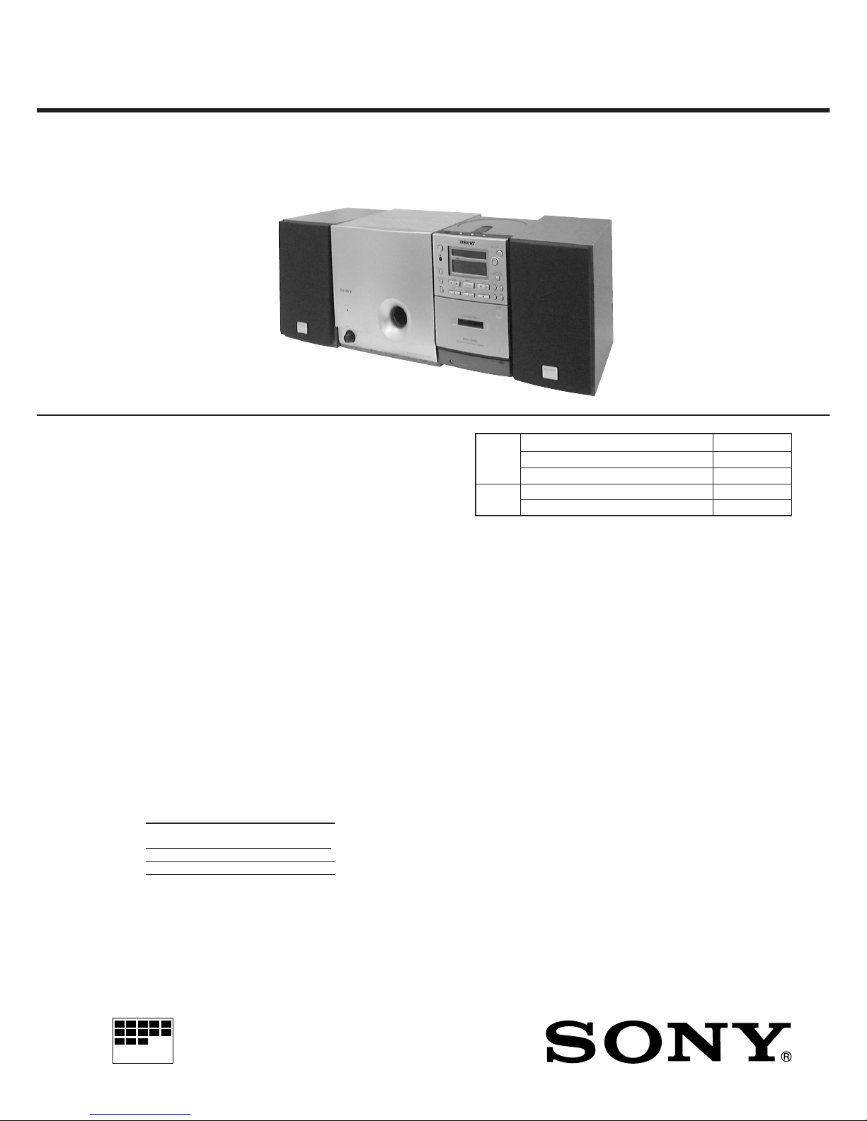
Sony PMC-D407L User manual

– 1 –
SERVICE MANUAL
AEP Model
PMC-D407L
PERSONAL COMPONENT SYSTEM
CD player section
System
Compact disc digital audio system
Laser diode properties
Material: GaAlAs
Wave length: 780 nm
Emission duration: Continuous
Laser output: Less than 44.6 µW
(This output is the value measured at a distance of
about 200 mm from the objective lens surface on
the optical pick-up block with 7 mm aperture.)
Spindle speed
200 r/min (rpm) to 500 r/min (rpm) (CLV)
Number of channels
2
Frequency response
20 - 20,000 Hz +1/–2.5 dB
Wow and flutter
Below measurable limit
Radio section
Frequency range
FM Except Italian model 87.6 - 107 MHz
Italian model 87.5 - 108 MHz
MW 531 - 1,602 kHz
LW 153 - 279 kHz
IF FM: 10.7 MHz
MW/LW: 450 kHz
Aerials
FM: External aerial terminal
MW/LW: External aerial terminal
– Continued on next page –
Cassette-corder section
Recording system
4-track 2-channel stereo
Fast winding time
Approx. 130 s (sec.) with Sony cassette C-60
Frequency response
TYPE I (normal): 40 - 15,000 Hz
Super woofer
Speaker
Woofer: 10 cm (4 in.) dia., 4.0 ohms, cone type
Power output
30 W (at 100 Hz)
Power consumption
AC 30 W
Dimensions (incl. projecting parts)
Approx. 210 ×210 ×247 mm (w/h/d)
(8 3/8 ×8 3/8 ×9 3/4 inches)
MassApprox. 4.1 kg (9 lb. 1 oz.)
CD Model Name Using Similar Mechanism PMC-D307L
Section CD Mechanism Type KSM-213CDM
Optical Pick-up Name KSS-213C
Tape Model Name Using Similar Mechanism PMC-D307L
Section Tape Transport Mechanism Type MF-D307
SPECIFICATIONS
MICROFILM
Ver 1.0 1998. 09

– 31 – – 32 –
PMC-D407L
6-7. SCHEMATIC DIAGRAM —TUNER SECTION — • Refer to page 63 for IC Block Diagrams.
• Waveforms
1
2
IC1 !£ (VCO)
IC2 1(X OUT)
1.4Vp-p
2.2µs
1.4Vp-p
75kHz
(Page 47)
(Page 47)
(Page 36)
(Page 46)

6-9. SCHEMATIC DIAGRAM — RDS SECTION — • Refer to page 64 for IC Block Diagrams.
– 35 – – 36 –
PMC-D407L
Note:
• All capacitors are in µF unless otherwise noted. pF: µµF
50 WV or less are not indicated except for electrolytics
and tantalums.
• All resistors are in Ωand 1/4W or less unless otherwise
specified.
•U: B+ Line.
• Voltage is dc with respect to ground under no-signal
(detuned) condition.
no mark : FM
( ) : MW
• Voltages are taken with aVOM(Inputimpedance10MΩ).
Voltage variations may be noted due to normal produc-
tion tolerances.
(Page 32)
(Page 47)

– 39 – – 40 – – 41 –
PMC-D407L
6-11. SCHEMATIC DIAGRAM — CD SECTION — • Refer to page 65 for IC Block Diagrams.
Note:
• All capacitors are in µF unless otherwise noted. pF: µµF
50 WV or less are not indicated except for electrolytics
and tantalums.
• All resistors are in Ωand 1/4W or less unless otherwise
specified.
•U: B+ Line.
•H: adjustment for repair.
• Voltage and waveforms are dc with respect to ground
under no-signal conditions.
no mark : CD STOP
• VoltagesaretakenwithaVOM(Inputimpedance10MΩ).
Voltage variations may be noted due to normal produc-
tion tolerances.
• Waveforms are taken with a oscilloscope.
Voltage variations may be noted due to normal produc-
tion tolerances.
• Circled numbers refer to waveforms.
• Signal path.
J: CD
c: digital out
Note: The components identified by mark !or dotted line
with mark !are critical for safety.
Replace only with part number specified.
• Waveforms
1
2
3
4
5
IC701 #¡ (RFO)
IC701 $¢ (TI)
IC701 2(FI)
IC702 @º (LRCK)
IC702 @™ (BCK)
6
IC702 @∞(XPCK)
7
IC702 #∞(XTAO)
1.3±0.2Vp-p
Approx. 50mVp-p
Approx. 50mVp-p
5Vp-p
22.6µs
6.7Vp-p
280ns
4.8Vp-p
240ns
4.8Vp-p
16.9344MHz
(Page 52)
(Page 45)
(Page 46)

– 45 – – 46 – – 47 –
PMC-D407L
6-13. SCHEMATIC DIAGRAM — MAIN SECTION — • Refer to page 64 for IC Block Diagrams.
Note:
• All capacitors are in µF unless otherwise noted. pF: µµF
50 WV or less are not indicated except for electrolytics
and tantalums.
• All resistors are in Ωand 1/4W or less unless otherwise
specified.
•C: panel designation.
•U: B+ Line.
• Voltages are dc with respect to ground under no-signal
(detuned) conditions.
no mark : FM
( ) : PB
< > : REC
[ ] : CD
∗: Impossible to measure
• VoltagesaretakenwithaVOM(Inputimpedance10MΩ).
Voltage variations may be noted due to normal produc-
tion tolerances.
• Signal path.
F: FM
E: PB
a: REC
L: LINE IN
J: CD
c: digital out
(Page 41) (Page 47)
(Page 32) (Page 41) (Page 51)
(Page 36)
(Page 61)
(Page 45)
(Page 31)
(Page 31)

– 51 – – 52 – – 53 –
PMC-D407L
6-15. SCHEMATIC DIAGRAM — CONTROL SECTION —
Note:
• All capacitors are in µF unless otherwise noted. pF: µµF
50 WV or less are not indicated except for electrolytics
and tantalums.
• All resistors are in Ωand 1/4W or less unless otherwise
specified.
•C: panel designation.
•U: B+ Line.
• Voltages and waveforms are dc with respect to ground
under no-signal (detuned) conditions.
no mark : FM
( ) : PB
< > : REC
[ ] : CD
• VoltagesaretakenwithaVOM(Inputimpedance10MΩ).
Voltage variations may be noted due to normal produc-
tion tolerances.
• Waveforms are taken with a oscilloscope.
Voltage variations may be noted due to normal produc-
tion tolerances.
• Circled numbers refer to waveforms.
3Vp-p
32.768kHz
4.9Vp-p
4.19MHz
• Waveforms
1
2
IC801 $º (XTAL1)
IC801 (£ (TEX)
12
(Page 46)
(Page 39)

– 57 – – 58 –
PMC-D407L
6-17. SCHEMATIC DIAGRAM —WOOFER SPEAKER SECTION — • Refer to page 64 for IC Block Diagrams.
Note:
• All capacitors are in µF unless otherwise noted. pF: µµF
50 WV or less are not indicated except for electrolytics
and tantalums.
• All resistors are in Ωand 1/4W or less unless otherwise
specified.
•C: panel designation.
•U: B+ Line.
• Voltages and waveforms are dc with respect to ground in
playback mode.
no mark : FM
• Voltages are taken with aVOM(Inputimpedance10MΩ).
Voltage variations may be noted due to normal produc-
tion tolerances.
Note: The components identified by mark !or dotted line
with mark !are critical for safety.
Replace only with part number specified.

6-19. SCHEMATIC DIAGRAM — POWER AMPLIFIER SECTION —
– 61 – – 62 –
PMC-D407L
Note:
• All capacitors are in µF unless otherwise noted. pF: µµF
50 WV or less are not indicated except for electrolytics
and tantalums.
• All resistors are in Ωand 1/4W or less unless otherwise
specified.
•2: nonflammable resistor.
•C: panel designation.
•U: B+ Line.
• Voltage and waveforms are dc with respect to ground
under no-signal (detuned) conditions.
no mark : FM
• Voltages are taken with aVOM(Inputimpedance10MΩ).
Voltage variations may be noted due to normal produc-
tion tolerances.
• Signal path.
F: FM
Note: The components identified by mark !or dotted line
with mark !are critical for safety.
Replace only with part number specified.
(Page 47)

– 63 – – 64 –
• IC Block Diagrams
IC1 TA2008AN
IC2 BU2615S
18 1314192021
10 11 1298765431 2
222324
AM
RF
FM
RF
BUFFBUFF
IF
BUFF
AF
BUFF
AM
IF
FM
IF
FM
OSC
AM
MIX AM
DET
AGC
FM
MIX
AM
OSC
17 16
1/8DIV
LEVEL
DET
FM
DET
ST
DET MUTE
FM MPX
15
AM/FM
ST/MONO
SW
2
19
11
18
17
20
13
1
16
15
3
4
5
6
7
PRESCALER MAIN COUNT
REFERENCE DIVIDER
I/O
CTL
8
14
SHIFT REGISTER LATCH
PHASE
DET
BUFFER
IF COUNT
CTL
20BIT COUNT
12109
ULLOCK
P5
PD1
PD2/P5
VDD1
VDD2
VSS
IF IN
P3
P4
P6
P2
P1
P0
CD
DA
CK
CE
AMIN
FMIN
XOUT
XIN
23 22 21
4 5 6321
2024
7dB
LOGIC
ALC1
DET
26dB
151617
987 10 11 12
1819 14 13
7dB
ALC2
26dB
15k 6k 6k
10k
10k
10k
10k
10k
10k
10k
10k
10k 10k 10k
10k
10k 10k
1k 1k
1k
1k
LINE
RADIO
RADIO
TAPE
TAPETAPE
LINE
IN1
INT
EXT
RADIO
IN1
RADIO
LINE
RADIO
IN2
TAPE
TAPE
LINE
IN2
MIC
IN
REC
PLAY
PRE
OUT1
PRE
OUT2
VCC
LINE
TAPE
BUF AMP
A2
BUF AMP
B1
BUF AMP
B2
BUF AMP
A1 MIC
AMP1
MUTE
MUTE
MUTE
ON
ON
ON
NAB
AMP2
MONITOR
AMP
MONITOR
AMP
NAB
AMP1
REC
AMP2
REC
AMP1
REF AMP 2.1
NAB
OUT1
NAB
NF1
REC
OUT1
NAB
IN1
NAB
IN2
REC
OUT2
NAB
NF2
NAB
OUT2
MIC
NF
VREF
GND
ALC
9 8 7 6 5 4 3 2 1
S
R
Q
B+
COMPARATOR
COMPARATOR
COMPARATOR
F.F.
PRE AMP
VCC
OUT
NOISE FILTER
MUTING
GND
NFB
IN
SENSE TIMING
PULSE WIDTH
IC301 TA2068N
IC404 BU1924F
IC305 BA338
IC601 TDA2052V
3 4 5 6 721
OUT
VDD
MUTE/
STANDBY
VEE
IN1+
IN–
IN2+
MUTE/
ST-BY
2
1
3
4
16
14
13
15
12
11
10
9
5
6
7
8
VREF
ANALOG
RCLK
(NC)
X2
X1
VDD2
VSS2
T1
T2
DIGITAL
QUAL
RDATA
VREF
MUX
VDD1
VSS1
VSS3
CMP
TEST
PLL
57KHz
RDS/ARI CLOCK
&
DRIVER
DEFFERENTIAL
DECODER
BIPHASE
DECODER
PLL
1187.5Hz
ANTI-ALIASING 8TH SWITCHED
CAPACITOR FILTER COMPARATOR

– 65 –
IC701 CXA1782BQ
36
PHD2
PHD1
PHD
33
LD
32
RF M
31
RF O
30
RF I
29
CP
28
CB
27
CC1
CC2
2526
FOK
24 SENS
23 C. OUT
22 XRST
21 DATA
20 XLT
19 CLK
18 VCC
17 ISET
16 SL 0
15 SL M
14 SL P
13
12
TA O
TA M
11
FSET
10
TG2
9
TGU
8
SRCH
7
FE M
6
FE O
5
FLB
4
FGD
3
FDFCT
2
FEI
1
FEO
48VC
47TDFCT
46TZC
45ATSC
44TEI
43LPFI
42TEO 41VEE
40EI
39E
38F
37FE BIAS
+
+
+
+
+
+
+ +
+
–
+
+
+
–
+
–
+
–
–
–
–
––
–
–
–
–
–
+
–
+
–
+
–
+
–
+
–
–
+
+
–
–
+
+
–
+
+
–
–
+
––
+
APC LEVELS
FOK
MIRR
DFCT
RF IV AMP2
RF IV AMP1
FE AMP
F IV AMP
E IV AMP
TE AMP
FZC COMP
BAL1
BAL2
BAL3
TOG1
TOG2
TOG3
TTL
IIL
IIL
TTL
TTL
IIL
• IIL DATA RESISTOR • INPUT SHIFT RESISTOR
• ADDRESS DECODER
• OUTPUT DECODER
HPF COMP LPF COMP
TZC COMP
DFCT
DFCT
TM1
FS4
ATSC
• WINDOW COMP
• FCS PHASE
COMPENSATION
• TRACKING
• PHASE
COMPENSATION
• ISET
FS1
FS2
TM4
TM5
TM6
TM3
TM7
TG2
• F SET
TG1
TM2
+
–
TOG1-3 FS1-4 TG1-2 TM1-7 PS1-4
BAL1-3
35 34

– 66 –
IC702 CXD2507AQ
IC703 BA6898FP
1
2
3
4
5
6
7
8
9
10
11
12
13
14
15
16
17
18
51
50
49
48
47
46
45
44
43
42
41
40
39
38
37
36
35
34
33
32313029282726252423222120
52535455565758596061626364
19
FOK
MON
MDP
MDS
LOCK
TEST
FILO
FILI
PCO
VSS
AVSS
CLTV
AVDD
RF
BIAS
ASYI
ASYO
ASYE
WDCK
DATA
XRST
SENS
MUTE
SQCK
SQSO
EXCK
SBSO
SCOR
VSS
WFCK
EMPH
DOUT
C4M
FSTT
XTSL
XTAO
XTAI
MNTO
SERVO AUTO
SEQUENCER
CPU
INTERFACE DIGITAL
CLV
SUB CODE
PROCESSOR
EFM
DEMODULATOR
DIGITAL
PLL
ASYMMETRY
CORRECTOR D/A
INTERFACE
ERROR
CORRECTOR
16K
RAM
DIGITAL
OUT
CLOCK
GENERATOR
LRCK
PCMD
BCLK
GTOP
XUGF
XPCK
VDD
GFS
RFCK
CZPO
XROF
MNT3
MNT1
XLON
SPOD
SPOC
SPOB
SPOA
CLKO
VDD
XLTO
DATO
CNIN
SEIN
CLOK
XLAT
3
5
14
4
5
3
6
D
LEVEL SHIFT
2728 26 25 24 23
21 3 4 5 6 7 8 9 10 11 12 13 14
LEVEL SHIFT
T. S. D.
REGULATOR, BIAS,
T. S. D. MONITOR
D D
18 17 16 15
LEVEL SHIFT
D
22
DD
LEVEL SHIFT
DD
DRIVER
MUTE
VCC
21 20 19
VCC NC
GND
OUT4 –
B
OUT4 –
A
IN4
IN4’
VREFIN
VCC
VCC
IN3’
IN3
OUT3 –
A
OUT3 –
B
NC
OPIN –B
OUT1 –B
OUT1 –A
IN1
RESET
REG –B
REGOUT
MUTE
GND
IN2’
IN2
OUT2 –A
OUT2 –B
GND
OPOUT

– 67 –
IC704 SM5877AM
ATTENUATION COUNTER
FILTER PROCESSOR &
ATTENUATION PROCESSOR
NOISE SHAPER
PROCESSOR BLOCK
INPUT INTERFACE
PWN DATA
PRODUCE
BLOCK
TIMING
CONTROL
123456789 10 11 12
13
14
15
16
17
18
19
202122
23
24
MUTE
DEEN
CKO
DVSS
BCKI
DI
DVDD
LRCI
TSTN
TO1
AVDDL
LO
AVSS
RO
AVDDR
MUTE
XVDD
XTI
XTO
XVSS
DS
RSTN
MODE
ATCK
L
L
L
R
R
R
Other manuals for PMC-D407L
1
Table of contents
Other Sony Speakers System manuals

Sony
Sony SS-XB3E User manual

Sony
Sony NSA-PE1 User manual

Sony
Sony SRS-A71 User manual

Sony
Sony WAHTSD1 - Rear Speaker Adaptor User manual

Sony
Sony HT-ST5 User manual

Sony
Sony TC-TX1 User manual

Sony
Sony SRS-PC45 User manual

Sony
Sony SRS-T70 User manual

Sony
Sony SRS-M30 User manual

Sony
Sony SS-B11H User manual

Sony
Sony HT-G700 User guide

Sony
Sony SS-W581T Instruction Manual

Sony
Sony SS-CT100D User manual

Sony
Sony SRS-A27 - Desktop Personal Speakers User manual

Sony
Sony SA-VA10 User manual

Sony
Sony HT-A7000 User guide

Sony
Sony SRS-D101 User manual

Sony
Sony SRS-A201 User manual

Sony
Sony HT-CT800 User manual

Sony
Sony SRS-A3 User manual