Sony SA-VA29 User manual

SAVA-29
US Model
Canadian Model
E Model
SERVICE MANUAL
HOME THEATER ACTIVE SPEAKER SYSTEM
MICROFILM
— Continued on next page —
SPECIFICATIONS
(Center) (Rear) (L-ch) (R-ch)
This unit is composed of the front speaker and the following units.
REAR SPEAKER
EXTERNAL CENTER SPEAKER SS-SR171
SS-CN15AV

— 2 —
TABLE OF CONTENTS
SAFETY-RELATED COMPONENT WARNING!!
COMPONENTS IDENTIFIED BY MARK !OR DOTTED LINE WITH
MARK !ON THE SCHEMATIC DIAGRAMS AND IN THE PARTS
LIST ARE CRITICAL TO SAFE OPERATION. REPLACE THESE
COMPONENTS WITH SONY PARTS WHOSE PART NUMBERS
APPEAR AS SHOWN IN THIS MANUAL OR IN SUPPLEMENTS
PUBLISHED BY SONY.
ATTENTION AU COMPOSANT AYANT RAPPORT
À LA SÉCURITÉ!
LES COMPOSANTS IDENTIFÉS PAR UNE MARQUE !SUR LES
DIAGRAMMESSCHÉMATIQUES ETLALISTEDESPIÈCESSONT
CRITIQUES POUR LA SÉCURITÉ DE FONCTIONNEMENT. NE
REMPLACER CES COMPOSANTS QUE PAR DES PIÈSES SONY
DONT LES NUMÉROS SONT DONNÉS DANS CE MANUEL OU
DANS LES SUPPÉMENTS PUBLIÉS PAR SONY.
TEST MODE······································································ 3
1. GENERAL ·········································································· 4
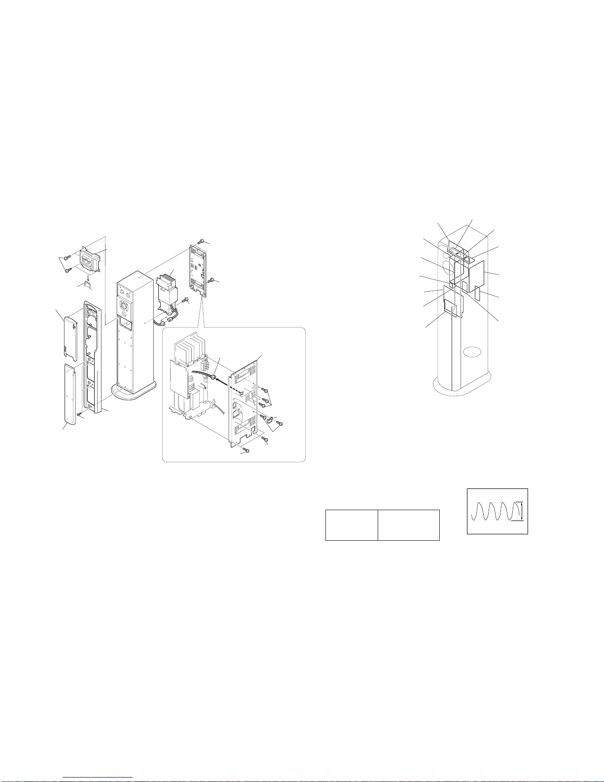
2. DISASSEMBLY
2-1. Removal Amplifier Block ··················································· 5
3. DIAGRAMS
3-1. Circuit Boards Location ····················································· 6
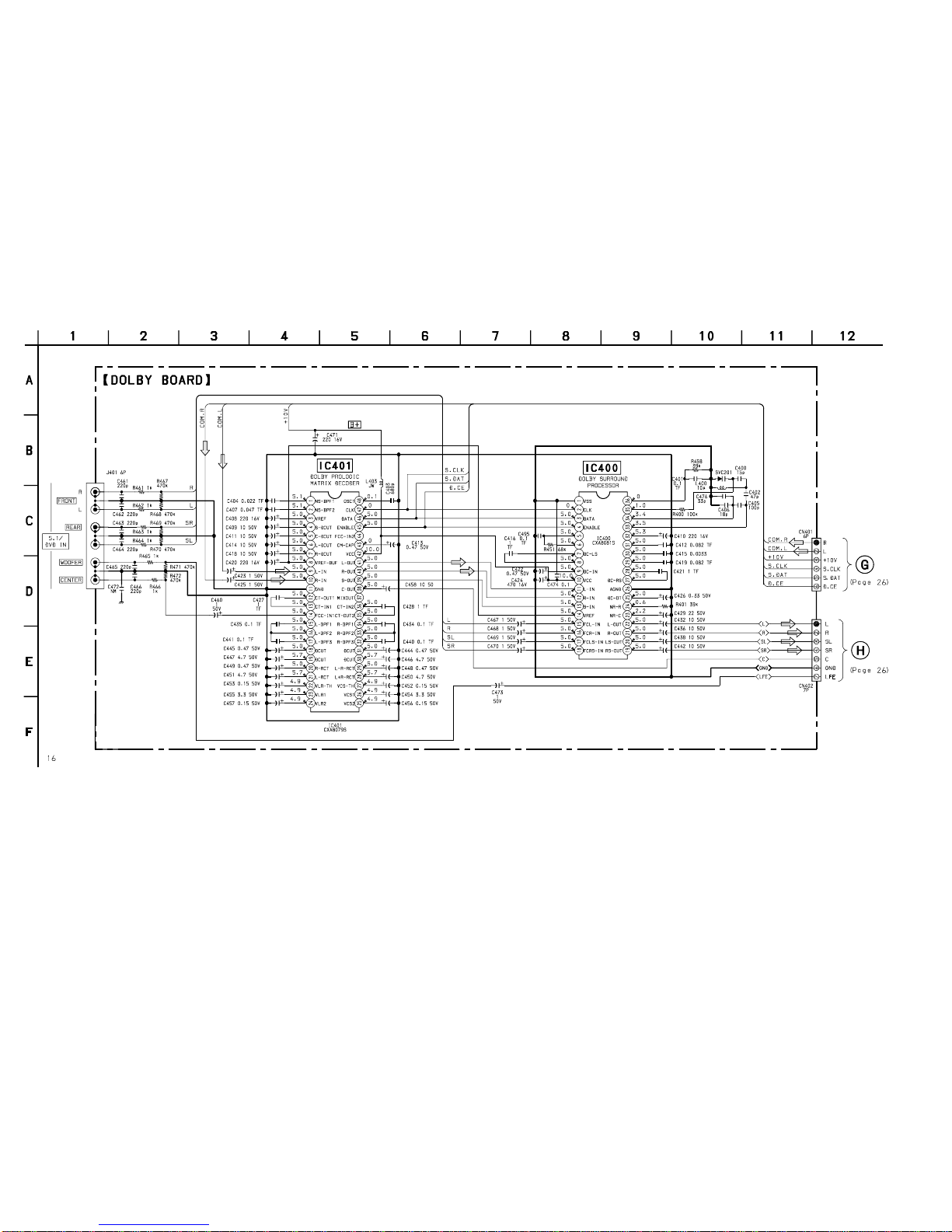
3-2. Schematic Diagram —Dolby Section — ··························· 7
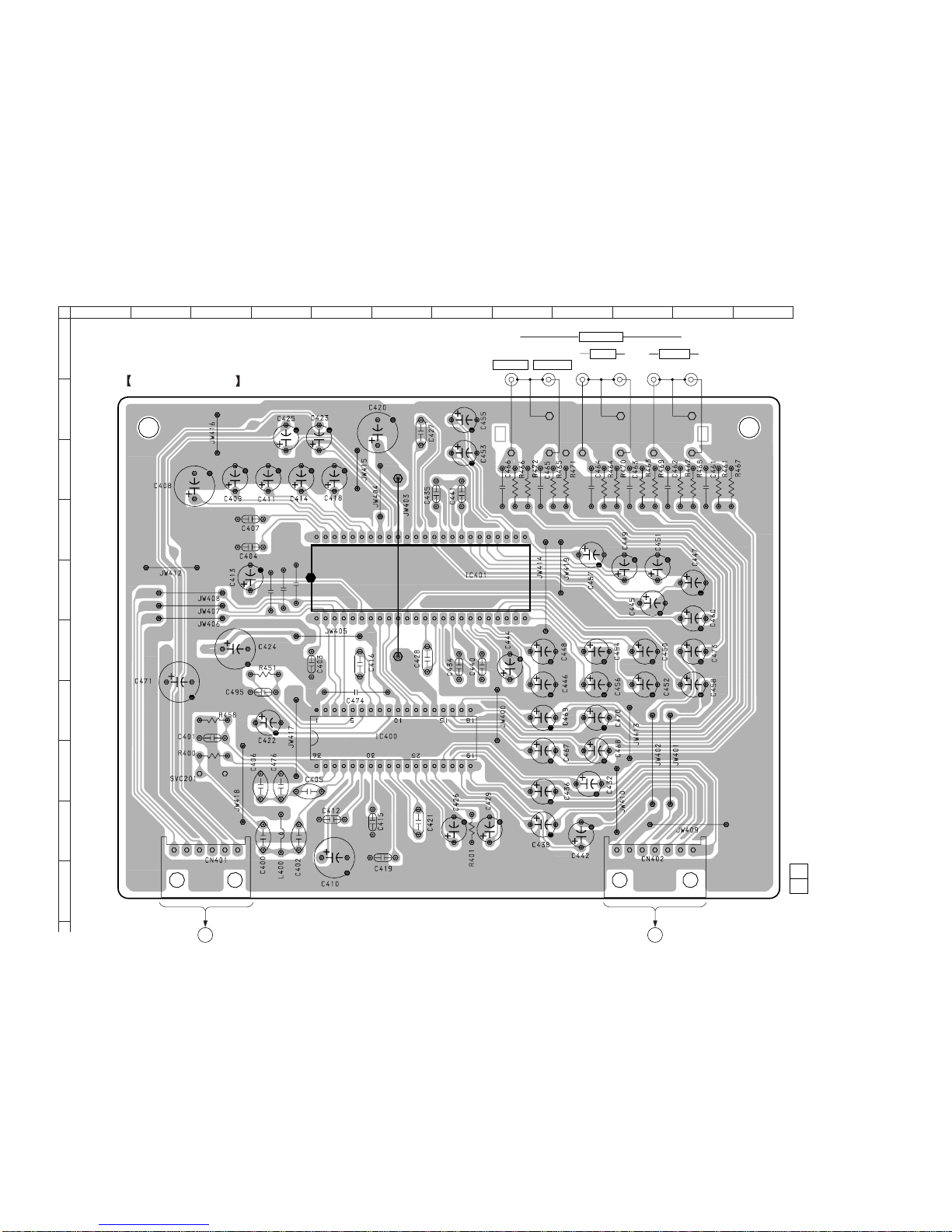
3-3. Printed Wiring Board —Dolby Section —························· 9
3-4. Schematic Diagram —Display Section — ······················· 11
3-5. Printed Wiring Board —Display Section — ···················· 13
3-6. Schematic Diagram —Power Section — ························· 15
3-7. Printed Wiring Board —Power Section — ······················ 17
3-8. Schematic Diagram —Power Transformer Section — ···· 19
3-9. Printed Wiring Board —Power Transformer Section —·· 21
3-10. Printed Wiring Board —Main Section — ························ 23
3-11. Schematic Diagram—Main Section (1/2) — ··················· 25
3-12. Schematic Diagram —Main Section (2/2) — ················· 27
3-13. IC Pin Function ································································ 29
3-14. IC Block Diagrams ··························································· 30
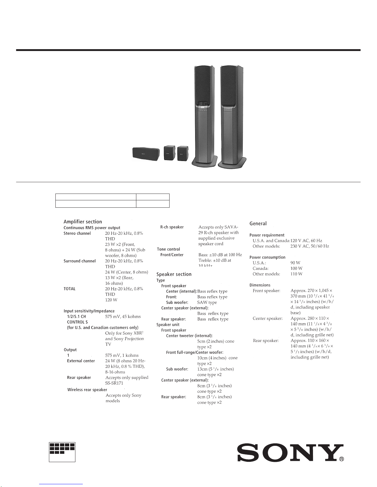
4. EXPLODED VIEWS
4-1. System (L) Assy ······························································· 32
4-2. System (R) Assy ······························································· 33
4-3. Amplifier Section ····························································· 34
4-4. Rear Speaker Section························································ 35
4-5. Center Speaker Section ···················································· 36
5. ELECTRICAL PARTS LIST ······································· 37
After correcting the original service problem, perform the
following safety checks before releasing the set to the customer:
Check the antenna terminals, metal trim, “metallized” knobs, screws,
and all other exposed metal parts forAC leakage. Check leakage as
described below.
LEAKAGE
TheAC leakage from any exposed metal part to earth ground and
from all exposed metal parts to any exposed metal part having a
return to chassis, must not exceed 0.5 mA (500 microampers).
Leakage current can be measured by any one of three methods.
1. A commercial leakage tester, such as the Simpson 229 or RCA
WT-540A. Follow the manufacturers’instructions to use these
instruments.
2. A battery-operated AC milliammeter. The Data Precision 245
digital multimeter is suitable for this job.
3. Measuring the voltage drop across a resistor by means of a
VOM or battery-operatedAC voltmeter. The “limit” indication
is 0.75 V, so analog meters must have an accurate low-voltage
scale. The Simpson 250 and Sanwa SH-63Trd are examples of
a passive VOM that is suitable. Nearly all battery operated
digital multimeters that have a 2V AC range are suitable. (See
Fig. A)
SAFETY CHECK-OUT
To Exposed Metal
Parts on Set
0.15
µ
F 1.5k
Ω
AC
voltmeter
(0.75V)
Earth Ground
Fig.A. Using an AC voltmeter to check AC leakage.

— 3 —
TEST MODE
MODE ALL FLUORESCENT INDICATOR TUBES
LIGHT
When theAC plug is inserted to the power outlet with pressing the
MASTERVOL + buttonand S.WOOFER button displayedmodel
name, after the all fluorescent indicator tubes light.
KEY CHECK MODE
1. Pull out the AC plug from the power outlet and turn the power
OFF.
2. Connect the lead wire to TP3 and TP4 on the KEY board.
3. Insert the AC plug to the power outlet and set to STANDBY
mode.
4. Let the lead wire short TP3 and TP4.
5. Fluorescentindicatortubedisplayed“KEYCHK 29” , andenter
the key check mode.
6. Pressing any buttons, the number of button will be displayed on
the fluorescent indicator tube.
7. After all buttons are pressed, it will be in the STANDBY mode.
Note:
1. The LED (D505)lights while pressing each button.
The LED lights in red when even number of buttons are pressed,
and it lights in green when odd number of buttons are pressed.
2. The LED lights even when the pressed button is pressed again.
CN552
IC513
TP2 TP4
TP1 TP3 S505
S506
Button
I / u
MASTER VOL –
MASTER VOL +
INPUT
SURROUND
CENTER MODE
S.WOOFER
Button Number
1
2
3
4
5
6
7
LED Color
Red
Green
Red
Green
Red
Green
Red
AMP CHECK MODE
1. Pull out the AC plug from the power outlet and turn the power
OFF.
2. Connect the lead wire to TP1 and TP2 on the KEY board.
3. Insert the AC plug to the power outlet and set to STANDBY
mode.
4. Let the lead wire connected TP1 and TP2.
5. Fluorescent indicator tube displayed “AMP CHK 29” or “AMP
CHK 59”, and enter the amp check mode.
6. The chek step advances in order as TP1 and TP2 are shorted.
7. To exit the test mode, disconnect theAC plug from power outlet.
AMP CHK 29 or 59
AMP CHK 1
AMP CHK 2
AMP CHK 3
AMP CHK 4
AMP CHK 5
AMP CHK 6
AMP CHK 7
AMP CHK 8
AMP CHK 9
AMP CHK 10
AMP CHK 11
AMP CHK 12
AMP CHK 13
STEP
0
1
2
3
4
5
6
7
8
9
10
11
12
13
INPUT
1
1
1
1
1
1
1
1
1
1
2
2
5.1
2
SW MODE
1
OFF
OFF
OFF
OFF
OFF
OFF
OFF
1
2
1
1
1
1
SUR MODE
PRO LOGIC
OFF
OFF
OFF
PRO LOGIC
PRO LOGIC
PRO LOGIC
GAME
OFF
OFF
PRO LOGIC
PRO LOGIC
–
PRO LOGIC
BASS
0
0
–5
+5
–5
+5
0
0
0
0
0
0
0
0
TREBLE
0
0
–5
+5
–5
+5
0
0
0
0
0
0
0
0
• Parts Location
[KEY BOARD] — SOLDELING side —
VOL
MIN
MAX
MAX
MAX
MAX
MAX
MAX
MAX
MIN
MAX
MAX
MAX
MAX
MAX
* The step 13 is theAUTO POWER ON/OFF check.
*

— 4 —
SECTION 1
GENERAL
1LEFT CHANNEL SPEAKER/CENTER
CHANNEL WOOFER
2CENTER CHANNEL TWEETERS
3RIGHT CHANNEL SPEAKER/CENTER
CHANNEL WOOFER
4SUPER WOOFER
5REAR SPEAKER
6EXTERNAL CENTER SPEAKER
1
2
3
44
5
26
REMOTE COMMANDER
FRONT SPEAKER (L-CH)

SAVA-29
— 6 —
— 5 —
SECTION 2
DISASSEMBLY SECTION 3
DIAGRAM
3-1. CIRCUIT BOARDS LOCATION
• Waveforms
For schematic diagrams.
Note:
• All capacitors are in µF unless otherwise noted. pF: µµF
50 WV or less are not indicated except for electrolytics
and tantalums.
• All resistors are in Ωand 1/4W or less unless otherwise
specified.
• % : indicates tolerance.
•¢: internal component.
•2: nonflammable resistor.
•1: fusible resistor.
•C: panel designation.
•U: B+ Line.
•V: B– Line.
• Voltages and waveforms are dc with respect to ground
under no-signal (detuned) conditions.
• Voltagesaretaken with a VOM (Inputimpedance 10MΩ).
Voltagevariationsmay be noted due tonormal production
tolerances.
• Waveforms are taken with a oscilloscope.
• Circled numbers refer to waveforms.
THIS NOTE IS COMMON FOR PRINTED WIRING
BOARDS AND SCHEMATIC DIAGRAMS.
(In addition to this necessary note is printed in each
block.)
Note:
The components identified
bymark !or dottedlinewith
mark!are critical for safety.
Replace only with part
number specified.
Note:
Lescomposants identifiés parune
marque !sont critiques pour la
sécurité.
Ne les remplacer que par une
piéce portant le numéro spécifié.
• Signal path.
F: AUDIO
• Abbreviation
CND : Canadian
SP : Singapore
MY : Malaysia
For printed wiring boards.
Note:
•X: parts extracted from the component side.
•b: Pattern from the side which enables seeing.
2
IC501#∞ (X2)
5.0 MHz 5.6Vp-p
4
Front panel assy
7
Display panel assy
6
Flat type wire
5
Four screws
(4
×
20)
1
Grill frame assy
2
Ornament frame
3
Three screws
(4
×
20)
!•
!¶
Screw
(M4
×
16)
9
Two screws
(M4
×
16)
8
Three screws
(4
×
25)
!ª
Amplifier
!∞
Connector
!§
Back panel
!º
Seven screws
(+BVTP 3
×
8)
!¡
Two screws
(+BVTP 3
×
8)
!£
Five screws
(+BVTP 3
×
8)
!¢
Two screws
(M4
×
16)
!™
POWER board
PS board
MAIN board
KEY board
DOLBY board
DISPLAY board
REG board
INPUT board
POW-SR board
T2 board
T1 board
POW-CSW board
POW-LR board
2-1. REMOVAL AMPLIFIER BLOCK (FRONT SPEAKER: L-CH)

SAVA-29
— 8 —
— 7 —
3-2. SCHEMATIC DIAGRAM — DOLBY SECTION — • See page 30 for IC Block Diagrams.

SAVA-29
— 10 —
— 9 —
3-3. PRINTED WIRING BOARDS — DOLBY SECTION — • See page 6 circuit boards location.
12
A
B
C
D
E
F
G
H
I
J
3456789101112
G H
1-670-184-
11
(11)
DOLBY BOARD
CENTER REAR
WOOFER RLRL
1716
124
2548
16
FRONT
5.1/DVD IN
J401
(Page 24) (Page 24)

SAVA-29
— 12 —
— 11 —
3-4. SCHEMATIC DIAGRAM — DISPLAY SECTION — • See page 6 for Waveforms. • See page 29 for IC Pin Functions.

SAVA-29
— 14 —
— 13 —
3-5. PRINTED WIRING BOARDS — DISPLAY SECTION — • See page 6 circuit boards location.
Ref. No. Location
D501 G-2
D502 G-2
D503 F-3
D504 E-11
D505 E-11
D506 G-4
D507 G-3
IC501 C-3
IC502 G-4
IC503 C-12
Q501 F-3
Q504 B-1
Q505 C-1
Q506 E-1
• Semiconductor
Location
12
A
B
C
D
E
F
G
H
34567891011121314
DISPLAY BOARD
KEY BOARD
D
1-670-185-
11
(11)
1-670-186-
11
(11)
FL501
(FLUORESCENT INDICATOR TUBE)
1
13
9
KK
A
(STANDBY)
MASTER VOL
S.WOOFER
SURROUNDINPUT CENTER
MODE
ON(GREEN)/READY
E
E
E
E
1
3
19
16
(Page 24)

SAVA-29
— 16 —
— 15 —
3-6. SCHEMATIC DIAGRAM — POWER SECTION —

SAVA-29
— 18 —
— 17 —
3-7. PRINTED WIRING BOARDS — POWER SECTION — • See page 6 circuit boards location.
Ref. No. Location
D631 H-11
D632 H-11
D701 H-9
IC601 A-10
IC602 A-12
IC603 A-8
IC604 A-6
IC605 A-4
IC606 A-2
• Semiconductor
Location
12
A
B
C
D
E
F
G
H
I
345678910111213
F
E C
1-670-189-
11
(11)
11
(11)
POW-SR BOARD
POWER BOARD
POW-CSW BOARD POW-LR BOARD
13
1
24
51
24
51
24
51
24
51
24
51
24
5
1-670-1901-670-1911-670-192
16
(Page 21)
(Page 21)
(Page 24)

SAVA-29
— 20 —
— 19 —
3-8. SCHEMATIC DIAGRAM — POWER TRANSFORMER SECTION — • See page 30 for IC Block Diagrams.

SAVA-29
— 22 —
— 21 —
3-9. PRINTED WIRING BOARDS — POWER TRANSFORMER SECTION — • See page 6 circuit boards location.
Ref. No. Location
D901 D-4
D902 B-4
D903 B-5
D904 B-5
D905 B-5
D908 B-6
D909 B-7
D910 B-6
D911 C-4
D912 I-6
D913 B-7
IC701 I-6
IC904 F-6
IC905 E-6
IC906 D-6
Q902 B-7
Q903 D-4
• Semiconductor
Location
12
A
B
C
D
E
F
G
H
I
J
34567891011121314
A
FE
B
1-670-183- 11
(11)
PS BOARD T2 BOARD T1 BOARD
AC
IN
T900
POWER
TRANSFORMER
1-670-187- 11
(11)
1-670-188- 11
(11)
F901
F902
F903
1
1
8
9
E
E
18
1
3
1
3
1
3
S701
CENTER
SPEAKER
110
1
5
1
11 1663
8
R-CH
SPEAKER
OUTLET
L-CH
SPEAKER
OUTLET
RL
J702
REAR
SPEAKER
J701
EXTERNAL
CENTER
SPEAKER
16
(Page 17) (Page 17)
(Page 24)
(Page 24)

SAVA-29
— 24 —
— 23 —
3-10. PRINTED WIRING BOARDS — MAIN SECTION — • See page 6 circuit boards location.
Ref. No. Location
D101 E-6
D102 E-6
D303 F-12
D804 G-2
D805 G-11
D806 G-11
D807 G-12
D808 G-12
D921 B-6
IC103 E-5
IC201 D-4
IC251 G-4
IC301 E-11
IC302 F-11
IC303 E-10
IC304 F-9
IC305 E-9
IC903 A-4
Q301 D-8
Q321 D-12
Q322 F-12
Q331 D-11
Q341 D-11
Q342 E-12
Q351 D-9
Q352 E-12
Q353 C-9
Q361 D-10
Q362 E-12
Q803 G-11
Q804 G-11
Q921 B-5
Q922 B-6
• Semiconductor
Location
12
A
B
C
D
E
F
G
H
I
345678910111213
C
1-670-181-
11
(11)
1-670-182- 11
(11)
1-670-196-
11
(11)
IN
IN
OUT
R
L
R
L
R
L
MAIN BOARDINPUT BOARD
REG BOARD
1
1
3
3
1
3
A
B
D
G
H
1
1
9
6
E
E
E
EE EE
E
E
E
E
1
5
1
4
58
1
4
58
1
4
58
1
4
58
E
E1
9
1
6
18
916
E
E
1
11 12
22
23
33
34
44
1
11
12
22
23
33 34
44
14
58
16
ON
OFF
S801
J801
VOLUME
SYNCHRO
WIRELESS
REAR SPEAKER
(TRANSMITTER)
CONTROL S
TV IN
1
2
J101
J103
(Page 10) (Page 18)
(Page 21)
(Page 21)
(Page 13)
(Page 9)

SAVA-29
— 26 —
— 25 —
3-11. SCHEMATIC DIAGRAM — MAIN SECTION (1/2) — • See page 30 for IC Block Diagrams.

SAVA-29
— 28 —
— 27 —
3-12. SCHEMATIC DIAGRAM — MAIN SECTION (2/2) — • See page 30 for IC Block Diagrams.

— 29 —
3-13. IC PIN FUNCTIONS
• IC501 SYSTEM CONTROL (uPD78043FGF-046-3B9) (DISPLAY BOARD)
Pin No.
1 to7
8
9
10
11
12
13
14
15
16
17
18
19
20
21
22
23
24
25
26
27
28
29
30
31
32
33
34
35
36
37
38
39
40
41
42
43
44
45
46
47
48
49
50
51
52
53 to 70
71
72 to 77
78 to 80
I/O
O
O
O
O
O
O
O
O
O
I
O
O
O
O
I
I
I
I
I
O
O
I
I
I
I
O
O
O
O
O
O
Description
FL grid output signal
Power supply (+5 V)
Power relay control output
Surround IC (LA2787, LV1017) control, chip enable output
CSW channels volume IC (LC75373) control, chip enable output
LR channels volume IC (LC75373) control, chip enable output
Rear volume IC (TC9210) control, latch output
Clock output
Data output
FL power supply switch
Reset input
Not used (Connected to ground)
A/D converter ground (Connected to ground)
LR mute
Center mute
Rear mute
Sub woofer mute
POWER key detection
Key input 1
Key input 0
Auto power signal detection input
A/D converter analog power supply (+5V)
A/D converter reference voltage
Stop detection
Not used (Not connected)
Ground (Connected to ground)
External crystal oscillator is connected to this terminal
Not used (Not connected)
Wireless rear power transmission control output
Sub woofer volume adjustment control output
SAVA-29/59 discrimination input
External/internal center speaker selection control input
Control S (TV) select control input
Not used (Connected to ground)
SIRCS data input
Not used (Connected to ground)
STANDBY LED ON/OFF control output
READY LED ON/OFF control output
OPERATE LED ON/OFF control output
Power supply (+5 V)
FL segment output signal
FL pull down voltage (–35 V)
FL segment output signal
FL grid output signal
Pin Name
7G to 1G
VDD
POWER RY
SUR CE
VOL CSW CE
VOL LR CE
VOL3 LAT
S CLOCK
S DATA
FL SW
RESET
AVSS
LR MUTE
C MUTE
S MUTE
SW MUTE
POWER SW
KEY 1
KEY 0
AUTO SW
AVDD
AVREF
STOP
XT2
VSS
X1
X2
REAR POWER
S/W BOOST
U SET SW
C EXT SW
TV/SW
SIRCS
IC
STANDBY LED
READY LED
OPERATE LED
VDD
S24 to S7
VLOAD
S6 to S1
10G to 8G
• Abbreviation
FL : Fluorescent indicator signal

— 30 —
3-14. IC BLOCK DIAGRAMS
IC400 CXA8081S (DOLBY BOARD)
IC401 CXA8079S (DOLBY BOARD)
RB
RB
DC-RS
AGND
DC-OT
NR-R
NR-C
RS-OUT
LS-OUT
R-OUT
L-OUT
RB
VSS
CLK
DATA
ENABLE
DC-LS
DC-IN
VCC
L-IN
R-IN
S-IN
VREF
FCL-IN
FCR-IN
FCLS-IN
FCRS-IN
OSC
VDD
PDM
PDM-COUT SRA1-8K
20KH-L.P.F.
DEC
5K/7K-L.P.F.
B-NR
R-STEREO
VOL/MUTE
RS-TRIM
LS-TRIM
1 2 3 4 5 6 7 8 9 10 11 12 13 14 15 16 17 18
192021222324252627282930313233343536
INV-PHASE
R+DELAY
L+DELAY
-6dB
L+R
L-R
P
B
P
B
20K
20K
20K
20K
48
VCS2
VCS1
VCS-TH
L+R-RCT
L-R-RCT
DCUT
DCUT
R-BPF3
R-BPF2
R-BPF1
CT-OUT2
CT-IN2
MIXOUT
C-OUT
S-OUT
R-OUT
L-OUT
VCC
CM-CAP
FCC-IN2
ENABLE
DATA
CLK
OSC1
NS-BPF1
NS-BPF2
VREF
S-DCUT
C-DCUT
L-DCUT
R-DCUT
VREF-BUF
L-IN
R-IN
GND
CT-OUT1
CT-IN1
FCC-IN1
L-BRF1
L-BRF2
L-BRF3
DCUT
DCUT
R-RCT
VCR-TH
VCR1
VCR2
47 46 45 44 43 42 41 40 39 38 37 36 35 34 33 32 31 30 29 28
L+R-RECT
27 26 25
P.S
VCS-LOG
OSC DEC
N-GEN
N-BPF
N-OH
DIV
BAL-DET
BALCONT
VREF
VR VR
VCRX8
COMB-NET
CMODE SMUTE
C-TRIM
PB
PB
PBPB
R
B
R
B
R-B.P.F.
L-B.P.F.
L-R-RECT
R-RECT
L-RECT VLR-LOG
DUAL-TIME
P.S
24
23
2221
20
19
18
17
16
15
1413121110987654321

— 31 —
IC201, 251 LC75373ED (MAIN BOARD)
+
–
+
–
+
–
+
–+
–
+
–
+
–
+
–
+
–
+
–
+
–
+
–+
–
+
–
+
–
+
–
DECODER LATCH SHIFT
REGISTER CONTROL
–
+
+
–
12 3 45 6 7 8 9 10
20
19
18
17
16
15
14
13
12
11
21
22
2324252627282930313233
34
35
36
37
38
39
40
41
42
43
44
LSELO
L4
L3
L2
L1
VDD
R1
R2
R3
R4
RSELO
RVRIN
RCOM
RT1
RT2
RT3
RTOUT
RSIN
RS1
RS2
RS3
RSOUT
RFIN
RFOUT
RROUT
VSS
CL
DI
CE
VREF
LROUT
LFOUT
LFIN
LSOUT
LS3
LS2
LS1
LSIN
LTOUT
LT3
LT2
LT1
LCOM
LVRIN
2
3
4
5
116
15
14
13
12
611
710
89
VSS
OUT
VDD
IN
A-GND
NC
CS2
STB
DATA
CK
GND
CS1
NC
A-GND
IN
OUT
R-CH
L-CH L-CH
DATA
LATCH
CIRCUIT
R-CH
DATA
LATCH
CIRCUIT
LEVEL
SHIFT
CIRCUIT
LEVEL
SHIFT
CIRCUIT
SHIFT RESISTER
(13bit)
STROBE OSC
CIRCUIT
IC304 TC9210P (MAIN BOARD)
1 2 3 4 5 6 7 8
OVER LOAD DET
F/F
OFFSET DET
LATCH/
AUTORESET
V
CC
ON
MUTE
AC OFF
DET
V
CC
IC701 µPC1237HA (PS BOARD)

NOTE:
• -XX, -X mean standardized parts, so they may
have some differences from the original one.
• Items marked “*” are not stocked since they
are seldom required for routine service. Some
delayshouldbeanticipatedwhenorderingthese
items.
• Themechanical parts with no reference number
in the exploded views are not supplied.
• Hardware (# mark) list and accessories and
packing materials are given in the last of this
parts list.
SECTION 4
EXPLODED VIEWS
— 32 —
When indicating parts by reference number,
please include the board name.
The components identified by mark !or
dotted line with mark !are critical for safety.
Replace only with part number specified.
Les composants identifiés par une marque
!sont critiques pour la sécurité.
Ne les remplacer que par une pièce portant
le numéro spécifié.
4-1. SYSTEM (L) ASSY
Ref. No. Part No. Description Remarks Ref. No. Part No. Description Remarks
1 4-991-883-01 FRAME, ORNAMENT
2 X-4948-622-1 FRAME (L) ASSY, GRILLE
3 4-951-733-01 CATCHER
4 1-505-681-11 SPEAKER (5cm)
5 X-4948-623-1 PANEL ASSY, FRONT
6 1-505-680-11 SPEAKER (10cm)
7 4-914-430-11 SCREW (4 ×20), TAPPING
8 4-991-271-01 BUTTON (A)
*9 4-991-276-01 HOLDER, FL TUBE
*10 A-4414-392-A DISPLAY BOARD, COMPLETE
11 4-991-284-01 REFLECTOR
12 X-4950-407-1 PANEL ASSY, DISPLAY
13 4-991-275-01 WINDOW (IR)
*14 1-670-186-11 KEY BOARD
15 1-773-241-11 WIRE (FLAT TYPE) (25 CORE)
16 4-991-272-01 BUTTON (B)
*17 A-4411-125-A CABINET (L) ASSY, SPEAKER
18 4-973-511-21 COVER (W)
19 1-505-679-11 SPEAKER (13cm)
20 4-929-125-01 SCREW (M4 ×16), TAPPING
*21 4-900-169-01 PANEL (L), BACK (US)
*21 4-900-169-11 PANEL (L), BACK (CND)
*21 4-900-169-21 PANEL (L), BACK (SP, MY)
*22 4-976-741-01 COVER, BUTTON
FL501 1-517-673-11 INDICATOR TUBE, FLUORESCENT
• Abbreviation
CND : Canadian
SP : Singapore
MY : Malaysia
a
a
b
b
#3
6
5
FL501
9
8
7
4
2
17
16
7
13
12
7
15
14
#1 #2
#2
#5 #5
#5
#3
#3
#3 #3
#3
#3
21
7
20
3
3
3
11
10
19
18
17
20
22
Other manuals for SA-VA29
2
Table of contents
Other Sony Speakers System manuals

Sony
Sony SRS-A5S User manual

Sony
Sony SS-B1000 User manual

Sony
Sony SS-VZ10 User manual

Sony
Sony SA-VA29 User manual

Sony
Sony HT-500 - Home Theater In A Box Manual

Sony
Sony SRS-D5100 User manual

Sony
Sony HT-S350 User guide

Sony
Sony SA-VE835ED Installation instructions manual

Sony
Sony SS-RG60 User manual

Sony
Sony SRS-T88 - Speaker - 4 Watt User manual