Sony Aiwa CX-JS3 User manual

SERVICE MANUAL
TUNER
FM tuning range 87.5 MHz to 108 MHz
FM usable sensitivity (IHF) 16.8 dBf
FM antenna terminal 75 ohms (unbalanced)
AM tuning range 531 kHz to 1602 kHz
AM usable sensitivity 350 µV/m
AM antenna Loop antenna
AMPLIFIER
Power output Rated: 32 W + 32 W (6 ohms, T.H.D.
1 %, 1 kHz/DIN 45500)
Reference: 40 W + 40 W (6 ohms,
T.H.D. 10 %, 1 kHz/DIN 45324)
MUSIC POWER: 100 W +100 W
Total harmonic distortion 0.08 % (16 W, 1 kHz, 6 ohms, DIN
AUDIO)
Input VIDEO/AUX: 400 mV
Outputs SPEAKER: 6 ohms or more
PHONES: 32 ohms or more
CASSETTE DECK
Track format 4 tracks, 2 channels stereo
Frequency response 50 Hz – 8 kHz
Recording system AC bias
Heads Deck A: playback x 1
Deck B: recording/playback x 1,
erase x 1
Model Name Using Similar Mechanism CX-JN3
CD Mechanism Type CDM74S-K6BD72
CD Base Unit Name BU-K6BD72
Section Optical Block Name KSM-213DCP
Optical Pick-up Name KSS-213D
Tape deck Model Name Using Similar Mechanism CX-JN3
Section Tape Transport Mechanism Type CWM43FF13
COMPACT DISC DECK RECEIVER
AEP Model
UK Model
CX-JS3
Ver 1.2 2004.08
9-877-297-03 Sony Corporation
2004H05-1 Personel Audio Company
© 2004.08 Published by Sony Engineering Corporation
SPECIFICATIONS
CX-JS3 is the amplifier, CD player, tape deck
and tuner section in JAX-S3.
CD PLAYER
Laser Semiconductor laser (λ= 780 nm)
Emission duration:
continuous
D/A converter 1 bit dual
Signal-to-noise ratio 85 dB (1 kHz, 0 dB)
Harmonic distortion 0.05 % (1 kHz, 0 dB)
GENERAL
Power requirements 230 V AC, 50/60 Hz
Power consumption 65 W
Power consumption With ECO mode on: 0.25 W
in standby mode With ECO mode off: 15 W
Dimensions (W x H x D) 280 x 330 x 392.5 mm
Weight 6.6 kg
Specifications and external appearance are subject to change
without notice.
COPYRIGHT
Check copyright laws relevant to recordings from discs, tuner
or tape for the country where the unit is to be used.
Licensed by BBE Sound, Inc. under USP4638258, 5510752
and 5736897.

CX-JS3
2
Notes on chip component replacement
•Never reuse a disconnected chip component.
•Notice that the minus side of a tantalum capacitor may be dam-
aged by heat.
Flexible Circuit Board Repairing
•Keep the temperature of the soldering iron around 270 ˚C dur-
ing repairing.
•Do not touch the soldering iron on the same conductor of the
circuit board (within 3 times).
•Be careful not to apply force on the conductor when soldering
or unsoldering.
CAUTION
Use of controls or adjustments or performance of procedures
other than those specified herein may result in hazardous ra-
diation exposure.
SAFETY-RELATED COMPONENT WARNING!!
COMPONENTS IDENTIFIED BY MARK 0OR DOTTED
LINE WITH MARK 0ON THE SCHEMATIC DIAGRAMS
AND IN THE PARTS LIST ARE CRITICAL TO SAFE
OPERATION. REPLACE THESE COMPONENTS WITH
SONY PARTS WHOSE PART NUMBERS APPEAR AS
SHOWN IN THIS MANUAL OR IN SUPPLEMENTS PUB-
LISHED BY SONY.
The following caution label is located inside the unit.
This appliance is classified as
a CLASS 1 LASER product.
The CLASS 1 LASER
PRODUCT MARKING is
located on the rear exterior.
UNLEADED SOLDER
Boards requiring use of unleaded solder are printed with the lead-
free mark (LF) indicating the solder contains no lead.
(Caution: Some printed circuit boards may not come printed with
the lead free mark due to their particular size)
: LEAD FREE MARK
Unleaded solder has the following characteristics.
•Unleaded solder melts at a temperature about 40 ˚C higher than
ordinary solder.
Ordinary soldering irons can be used but the iron tip has to be
applied to the solder joint for a slightly longer time.
Soldering irons using a temperature regulator should be set to
about 350 ˚C.
Caution: The printed pattern (copper foil) may peel away if the
heated tip is applied for too long, so be careful!
•Strong viscosity
Unleaded solder is more viscou-s (sticky, less prone to flow)
than ordinary solder so use caution not to let solder bridges oc-
cur such as on IC pins, etc.
•Usable with ordinary solder
It is best to use only unleaded solder but unleaded solder may
also be added to ordinary solder.

CX-JS3
3
TABLE OF CONTENTS
1. SERVICING NOTES ................................................ 4
2. GENERAL
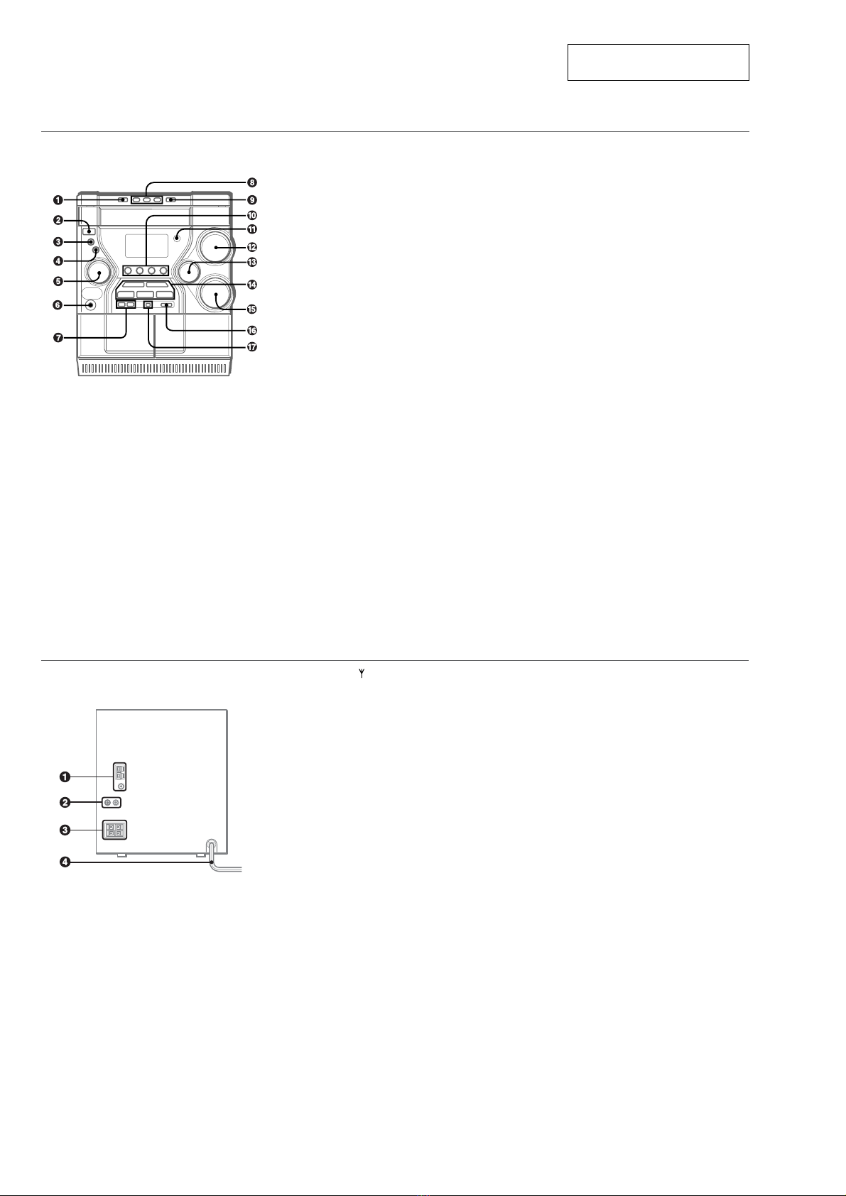
Location of Controls ....................................................... 6
3. DISASSEMBLY
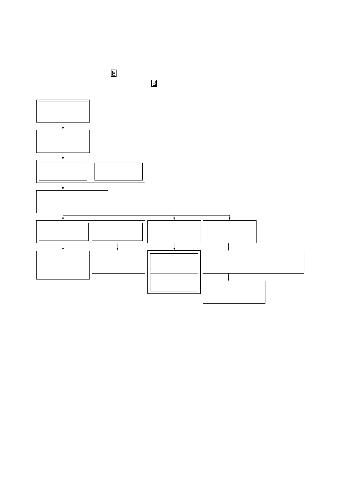
3-1. Disassembly Flow ........................................................... 8
3-2. Case (SIDE-L/R)............................................................. 9
3-3. Case (Top) ....................................................................... 9
3-4. Tray Panel........................................................................ 10
3-5. CD Mechanism Deck (CDM74S-K6BD72)................... 10
3-6. Front Panel Section ......................................................... 11
3-7. Mechanical Deck (CWM43FF13) .................................. 11
3-8. Rear Cabinet Section ...................................................... 12
3-9. PT Board, MAIN Board.................................................. 12
3-10. Table Assy ....................................................................... 13
3-11. Motor (TB) Board ........................................................... 13
3-12. Motor (LD) Board ........................................................... 14
3-13. Base Unit (BU-K6BD72)................................................ 14
3-14. Motor Gear Assy (Sled) (M701), BD Board .................. 15
3-15. Optical Pick-up (KSS-213D) .......................................... 15
4. TEST MODE.............................................................. 16
5. ELECTRICAL ADJUSTMENTS
CD Section ...................................................................... 17
6. DIAGRAMS
6-1. Block Diagram – CD Section – ..................................... 18
6-2. Block Diagram – TUNER/TAPE/PANEL Section –..... 19
6-3. Block Diagram –AMP/POWER SUPPLY Section – ... 20
6-4. Note for Printed Wiring Boards and
Schematic Diagrams ....................................................... 21
6-5. Printed Wiring Board – BD Section – ........................... 22
6-6. Schematic Diagram – BD Section – .............................. 23
6-7. Printed Wiring Boards – CHANGER Section –............ 24
6-8. Schematic Diagram – CHANGER Section – ................ 25
6-9. Schematic Diagram – MAIN Section (1/4) –................ 26
6-10. Schematic Diagram – MAIN Section (2/4) –................ 27
6-11. Schematic Diagram – MAIN Section (3/4) –................ 28
6-12. Schematic Diagram – MAIN Section (4/4) –................ 29
6-13. Printed Wiring Board – MAIN Section – ...................... 30
6-14. Printed Wiring Board – HP Section – ........................... 31
6-15. Schematic Diagram – HP Section – .............................. 31
6-16. Printed Wiring Board – PANEL Section – .................... 32
6-17. Schematic Diagram – PANEL Section – ....................... 33
6-18. Printed Wiring Boards – KEY Section –....................... 34
6-19. Schematic Diagram – KEY Section – ........................... 35
6-20. Printed Wiring Board – PT Section – ............................ 36
6-21. Schematic Diagram – PT Section –............................... 37
6-22. IC Pin Function Description ........................................... 41
7. EXPLODED VIEWS
7-1. Case Section .................................................................... 43
7-2. Front Panel Section-1...................................................... 44
7-3. Front Panel Section-2...................................................... 45
7-4. Front Panel Section-3...................................................... 46
7-5. Front Panel Section-4...................................................... 47
7-6. Chassis Section ............................................................... 48
7-7. CD Mechanism Deck Section-1
(CDM74S-K6BD72) ....................................................... 49
7-8. CD Mechanism Deck Section-2
(CDM74S-K6BD72) ....................................................... 50
7-9. CD Mechanism Deck Section-3
(CDM74S-K6BD72) ....................................................... 51
7-10. Base Unit Section (BU-K6BD72) .................................. 52
8. ELECTRICAL PARTS LIST ............................... 53

4
CX-JS3 SECTION 1
SERVICING NOTES
NOTES ON HANDLING THE OPTICAL PICK-UP
BLOCK OR BASE UNIT
The laser diode in the optical pick-up block may suffer electro-
static break-down because of the potential difference generated
by the charged electrostatic load, etc. on clothing and the human
body.
During repair, pay attention to electrostatic break-down and also
use the procedure in the printed matter which is included in the
repair parts.
The flexible board is easily damaged and should be handled with
care.
NOTES ON LASER DIODE EMISSION CHECK
The laser beam on this model is concentrated so as to be focused
on the disc reflective surface by the objective lens in the optical
pick-up block. Therefore, when checking the laser diode emis-
sion, observe from more than 30 cm away from the objective lens.
LASER DIODE AND FOCUS SEARCH OPERATION
CHECK
Carry out the “S curve check” in “CD section adjustment” and
check that the S curve waveforms is output three times.
HOW TO OPEN THE DISC TRAY WHEN POWER SWITCH TURNS OFF.
3
Pull-out the disc tray.
1
Remove the case (side-L).
2
Turn the loading gear in the direction of arrow
A
.
A

5
CX-JS3
SERVICE POSITION
– CD mechanism deck –
–Tape mechanism deck –
main board (CN691)
Connect wire (flat type) (19 core) to
main board (CN691) and BD board (CN710).
BD board (CN710)
Connect wire (flat type) (13 core) to
panel board (CN601) and mechanical deck.
panel board (CN601)
main board (CN301)

6
CX-JS3 SECTION 2
GENERAL This section is extracted from
instruction manual.
•LOCATION OF CONTROLS
1DISC CHANGE
Rotates the CD trays.
2POWER 6STANDBY/ON
Switches the unit on and off (standby).
The red indicator flashes when receiving a signal from
the remote.
3MODE
Selects various modes (ECO and Repeat/Shuffle/
Programmed playback, etc.) when used in combination
with ENTER and MULTI JOG.
4ENTER
Fixes the modes and the time (ECO, Repeat/Shuffle/
Programmedplayback,clock,andtimer,etc.)whenused
in combination with ENTER and MULTI JOG.
#TREBLE
Enhances high frequency sound.
$cPLAY/PRESET
When the unit is turned off: activates or deactivates
DEMO.
CD and Tape: starts playback.
Tuner: tunes into a preset station.
sSTOP/CLEAR
CD and Tape: stops playback.
Tuner: clears a station preset.
fTUNING DOWN, gTUNING UP
CD: searches a track in fast forward or fast reverse
playback when held down.
Tape: fast forwards or rewinds the tape.
Tuner: manually tunes down or up within the band.
aPAUSE/SET
CD and Tape: pauses playback.
Tuner: stores the received station in to preset.
%BASS
Emphasizes low frequency sound.
^i-Bass
Produces rich and clear low frequency sound.
&PTY
Displays a program type for RDS (Radio Data System)
Main unit: front
Refer to the pages indicated in parentheses for details.
5MULTI JOG
WhenusedincombinationwithENTERandMULTIJOG,
CD: selects a track and Repeat/Shuffle/Programmed
playback.
Tuner: selects a preset station.
Tape: specifies tape length.
Clock and Timer: sets the time.
i-Bass: selects a frequency range.
Spectrumanalyzer,ECO and Dimmer: selectsthemode.
6PHONES jack
Plug in here an optional headphones set with a mini
stereo plug (ø3.5 mm). Speaker output is canceled.
7SYNC DUB
Starts dubbing a whole tape.
wREC/REC MUTING
Starts recording.
8DISC DIRECT PLAY 1-3
Selects a disc.
9zOPEN/CLOSE
Opens or closes the disc compartment.
0TAPE A/B
Selects Tape function, and deck A or B.
TUNER/BAND
Selects Tuner function and the radio band.
VIDEO/AUX
Selectsthe function of externalequipment connected to
VIDEO/AUX jacks.
CD
Selects CD function.
!Remote sensor
Receives a signal from the remote.
@VOLUME
Adjusts the volume.
Main unit: rear
Refer to the pages indicated in parentheses for details.
1AM LOOP, FM 75 Ωterminals
Plug in the supplied AM and FM antennas here.
2VIDEO/AUX jacks
Acceptsanalog sound signals from external equipment.
Connect using an optional connecting cable with RCA
phono plugs (red plug to R jack, white plug to L jack).
Referalsototheoperatinginstructionsofyourequipment.
To switch function to external input, press VIDEO/AUX.
Tip:
To changethedisplayednameforthisfunction,turnthe
unit on, then hold down VIDEO/AUX and press POWER
on the unit. Repeat the procedure to select "VIDEO",
"AUX" or "TV".
3#SPEAKER terminals
Connectthe speaker cord of thesuppliedfrontspeakers
here.
4AC power cord

7
CX-JS3
Buttons with the same or similar names with the main unit
basically have the same function.
1POWER
21-0/10, +10
CD: selects a CD track of the specified number.
Tuner: tunes in to the station with the specified preset
number.
The numbered buttons take on these functions below when pressed
with SHIFT held down
:
EDIT
EntersAIEditRecordingorProgrammedEditRecording
mode when pressed in stop mode.
BAND
Selects Tuner function and the radio band.
TAPE A/B
SPECTRUM
Changes the spectrum analyzer display.
TUNER MODE
Switches between stereo or monaural FM reception.
3r,t
CD: selects a track.
Tuner: selects a preset station.
Tape: specifies tape length.
BASS and TREBLE: adjusts the level.
Clock and Timer: sets the time.
4PLAY MODE
SelectsShuffleorProgrammedplaybackinCDfunction.
REPEAT
Enters CD repeat playback mode.
ENTER
5CLOCK/TIMER/SET
Enters timer setting mode.
CLOCK/TIMER/SELECT
Selects timer playback, timer recording or timer off.
6DISPLAY
7SHIFT
Holddownwhen pressinga numberedbutton tochange
its function to that printed above the number.
e.g.)
"Press SHIFT+BAND on the remote" indicates "Hold
downSHIFTandpress'2'(BAND)".Doingsomakesyou
be able to select Tuner function and the radio band.
8FUNCTION
Switches the active function among CD, TAPE, TUNER
and VIDEO (AUX or TV).
9DISC SKIP
Select a disc.
0c/d
When the unit is turned off: activates or deactivates
DEMO.
CD and Tape: starts playback.
s
CD and Tape: stops playback.
f,g
CD: searches a track in fast forward or fast reverse
playback when held down.
Tape: fast forwards or rewinds the tape.
Tuner: manually tunes down or up within the band.
a
CD and Tape: pauses playback.
!SLEEP
Switchesthesleep-timeron/offandselectstheduration.
@VOLUME (+,-)
Adjusts the volume.
#SOUND
Selects BASS or TREBLE setting mode
CLEAR
Clears a track of the CD programmed playback and a
Radio preset station.
Note
Thebuttons not explained above(ALBUMN,Mand
KARAOKE) do not operate for this unit.
Remote control
Refer to the pages indicated in parentheses for details.
Setting the clock
Use the remote.
1
Press CLOCK/TIMER/SET.
Gotostep3whenthetimeappearsandthe'hour'flashes.
2
Press ror trepeatedly until "CLOCK
SET" appears in the display and then press
ENTER.
3
Press ror trepeatedly to set the hour
and then press ENTER.
4
Press ror trepeatedly to set the minute
and then press ENTER.
Thetime display stops flashing and theclock starts from
00 seconds.
•MULTI JOG is also available in place of ror t.
To display the time
PressDISPLAYon theremote. The time willbe displayed for
6 seconds.
If "- -:- -" appears when the unit is turned off
There has been a power interruption. Re-set the clock.

CX-JS3
8
• This set can be disassembled in the order shown below.
3-1. DISASSEMBLY FLOW
SECTION 3
DISASSEMBLY
Set
3-2. CASE
(SIDE-L/R)
(Page 9)
3-3. CASE (TOP)
(Page 9) 3-4. TRAY PANEL
(Page 10)
3-6. FRONT PANEL
SECTION
(Page 11)
3-8. REAR CABINET
SECTION
(Page 12)
3-7. MECHANICAL
DECK
(CWM43FF13)
(Page 11)
3-9. PT BOARD,
MAIN BOARD
(Page 12)
3-14. MOTOR GEAR ASSY (SLED) (M701),
BD BOARD
(Page 15)
3-15. OPTICAL PICK-UP
(KSS-213D)
(Page 15)
3-13. BASE UNIT
(BU-K6BD72)
(Page 14)
3-10. TABLE ASSY
(Page 13)
3-11. MOTOR (TB)
BOARD
(Page 13)
3-12. MOTOR (LD)
BOARD
(Page 14)
3-5. CD MECHANISM DECK
(CDM74S-K6BD72)
(Page 10)
Note 1: The process described in can be performed in any order.
Note 2: Without completing the process described in , the next process can not be performed.

CX-JS3
9
3-3. CASE (TOP)
Note: Follow the disassembly procedure in the numerical order given.
3-2. CASE (SIDE-L/R)
1
case screw
1
case screw
3
3
4
4
5
case (side-L)
5
case (side-R)
2
two screws
(BVTP3
×
10)
2
two screws
(BVTP3
×
10)
1
two case screw
s
1
two case screws
3
4
case (top)
2
claw
2
cla
w
1
two screws
(BVTP3
×
10)
2
claw
2
claw

CX-JS3
10
3-4. TRAY PANEL
3-5. CD MECHANISM DECK (CDM74S-K6BD72)
4
tray panel
2
Pull-out the disc table.
1
Turn the loading gear
in the direction of arrow
A
.
A
3
four claws
5
CD mechanism deck
(CDM74S-K6BD72)
3
screw
(BVTP3
×
10)
4
two screws
(BVTP3
×
10)
3
screw
(BVTP3
×
10)
1
wire (flat type) (19 core)
(CN691)
2
connector
(CN701)

CX-JS3
11
3-6. FRONT PANEL SECTION
3-7. MECHANICAL DECK (CWM43FF13)
1
screw
(BVWHTP)
2
headphone board
7
front panel section
5
three screws
(BVTP3
×
10)
3
wire (flat type) (11 core)
(CN694)
4
connector
(CN301)
4
connector
(CN302)
6
connector
(CN101)
5
ground mechanical plate
2
six screws
(BVTP3
×
10)
1
wire (flat type) (13 core)
4
mechanical deck
(CWM43FF13)
3
clamp

CX-JS3
12
3-8. REAR CABINET SECTION
3-9. PT BOARD, MAIN BOARD
3
rear cabinet section
2
three screws
(BVTP3
×
10)
2
screw
(BVTP3
×
10)
1
wire (flat type) (15 core) (CN802)
6
PT board
8
main board
4
Remove the PWB PT HLDR
in the direction of the arrow.
2
screw
(BVTT3
×
8)
7
screw
(BVTT3
×
8)
3
screw
(BVTP3
×
10)
5
two screws
(ITC4
×
8)
7
two screws
(BVTT3
×
8)
5
two screws
(ITC4
×
8)
1
connector (CN091)

CX-JS3
13
3-10. TABLE ASSY
3
wire (flat type) (5 core
)
(CN702)
4
hook
1
Turn the loading gear
in the direction of arrow
A
.
A
5
two claws
2
Pull-out the table assy.
6
table assy
3-11. MOTOR (TB) BOARD
2
table (loading)
4
connector
(CN731)
1
screw
(PTPWH M2.6)
5
two screws
(BTTP M2.6)
6
motor (TB) boar
d
3
belt (table)

CX-JS3
14
3-12. MOTOR (LD) BOARD
3-13. BASE UNIT (BU-K6BD72)
2
connector
(CN704)
3
two screws
(BTTP M2.6)
4
motor (LD) board
1
belt (loading)
3
four coil springs
(insulator)
4
four insulators
5
base unit
(BU-K6BD72
)
1
four screws
(BTTP M2.6)
2
four stoppers (BU)

CX-JS3
15
1
Remove two
solders.
qa
BD board
2
two screws
(P2
×
3)
6
claw
7
gear (A)
8
gear (B)
5
wire (flat type) (16 core
)
(CN708)
0
motor gear assy (SLED)
(M701)
3
screw (P2.6
×
6)
9
Remove two solders.
4
2
sled shaft
1
Slide the lever
in the direction of arrow
A
.
3
Remove the optical pick-up
(KSS-213D) in the direction
of arrow
B
.
A
B
3-14. MOTOR GEAR ASSY (SLED) (M701), BD BOARD
3-15. OPTICAL PICK-UP (KSS-213D)

16
CX-JS3 SECTION 4
TEST MODE
MC COLD RESET
•The cold reset clears all data including preset data stored in the
RAM to initial conditions. Execute this mode when returning
the set to the customer.
Procedure:
1. In the standby status, while pressing the xbutton, press the
[POWER] button.
2. The set is reset, then becomes standby status.
GC TEST MODE
Procedure:
1. Press the [POWER] button to turn the power on.
2. While pressing the xbutton, press the [POWER] button for
5 seconds.
3. It change displays in order of model type, version and suffix at
2 seconds interval, then the display is back to normal status.
AMP TEST MODE
Procedure:
1. In the status where AC plug is disconnected, while pressing
the [VIDEO/AUX] button, connect the AC plug to turn the
power on. Then enter the AMP test mode and display “AMP
TEST”.
2. If turn the [VOLUME] knob clockwise, it displays “VOLUME
MAX”, and if turn the knob counterclockwise, it displays
“VOLUME 0”.
3. If the [TREBLE] and [BASS] knobs are turned clockwise or
counterclockwise, it change displays in order of “EQ MAX”,
“EQ MIN” and “EQ FLAT”.
4. To release from this mode, disconnect the AC plug and turn
the power off.
DISC TRAY LOCK
Procedure:
1. Press the [POWER] button to turn the power on.
2. While pressing the xbutton, press the [ OPEN/CLOSE]
button for 5 seconds.
3. The message “LOCKED” is displayed and the tray is locked.
(Even if exiting from this mode, the tray is still locked)
4. To release this lock, while pressing the xbutton, press the
[ OPEN/CLOSE] button for 5 again.
5. The message “UNLOCKED” is displayed and the tray is un-
locked.
CD REPEAT 5 LIMIT CANCEL MODE
•Number of repeat for CD playback is 5 times when the repeat
mode is “REPEAT”. This mode enables CD to repeat playback
for limitless times.
Procedure:
1. Press the [POWER] button to turn the power on.
2. In the repeat on status, while pressing the xbutton, press the
[CD] button to enter the CD repeat 5 limit cancel mode and
repeat mark blinks on the fluorescent indicator tube.
3. To release this mode, press the [POWER] button to turn the
power off.
Z
Z
FUNCTION CHANGE MODE
•Select either TV, VIDEO orAUX (MD) of the external function
input.
Procedure:
1. Press the [POWER] button to turn the power on.
2. While pressing the [VIDEO/AUX] button, press the [POWER]
button.
3. Each time this operation is operated, it change displays in or-
der of “TV”, “VIDEO” and “AUX”.

CX-JS3
1717
CD SECTION
Note:
1. CDBlock is basically designed to operate without adjustment.Therefore,
check each item in order given.
2. UseYEDS-18 (3-702-101-01) unless otherwise indicated.
3. Use an oscilloscope with more than 10MΩimpedance.
4. Clean the object lens by an applicator with neutral detergent when the
signal level is low than specified value with the following checks.
S-CURVE CHECK
Procedure :
1. Connect an oscilloscope to TP (FE) and TP (VC).
2. Turn the power on.
3. Load a disc (YEDS-18) and actuate the focus search. (In
consequence of open and close the disc tray, actuate the focus
search)
4. Confirm that the oscilloscope waveform (S-curve) is
symmetrical betweenA and B.And confirm peak to peak level
within 3 ±0.5 Vp-p.
Note: •Try to measure several times to make sure than the ratio
of A : B or B : A is more than 10 : 7.
•Take sweep time as long as possible and light up the
brightness to obtain best waveform.
RF LEVEL CHECK
Procedure :
1. Connect an oscilloscope to TP (RF) and TP (VC).
2. Turn the power on.
3. Load a disc (YEDS-18) and playback.
4. Confirm that oscilloscope waveform is clear and check if RF
signal level is correct or not.
BD board Oscilloscope
TP(FE)
TP(VC)
symmetry
S-curve waveform
within 3
±
0.5Vp-p
A
B
TP(RF)
BD board oscilloscope
TP(VC)
Note: Clear RF signal waveform means that the shape “ ◊” can be clearly
distinguished at the center of the waveform.
Connecting Location: BD board
RF signal waveform VOLT/DIV : 200mV
TIME/DIV : 500ns
level : 1.0
±
0.3Vp-
p
SECTION 5
ELECTRICAL ADJUSTMENTS
CD TEST MODE
•This mode can run the CD sled motor freely. Use this mode, for
instance, when cleaning the pickup.
Procedure:
1. In the status where AC plug is disconnected, while pressing
the [CD] button, connect theAC plug to turn the power on.
2. When enter this mode, it displays “CD TEST” and few sec-
onds later, all segments turn on of the fluorescent indicator
tube.
3. To release from this mode, disconnect the AC plug and turn
the power off.
In this mode, it operates as following table.
Button Operation Purpose of use
MMove the pick-up to outside track Sled circuit check
mMove the pick-up to inside track Tracking circuit check
Mechanism operation check
Optical pick-up check
NPlayback a CD Servo block check
If it cannot focus on, it continuous focus search
xWhen playback a CD: stop playback APC circuit check
When stop a CD: Laser current measure
display “READING” (blink) Focus search waveform check
continuous laser diode on Tracking balance check
continuous focus search (not made focus on)
XPause, Tracking servo off
(ignore CLV error)
TP (VC) TP (RF)
TP (FE)
IC721
– BD Board (Conductor side) –

CX-JS3
1818
8
7
9
10
80
79
70 LIMIT SW
20
TDO
18
10
VO3(+)
FOIN
20TIN
3SPIN
7LDS
25SLIN
17 VO3(–)
11 VO2(+)
12 VO2(–)
26 VO4(+)
27 VO4(–)
2 VO1(+)
1 VO1(–)
A
C
B
D
E
F
LD
PD
CD DSP
IC721
21
FDO
23
SLDO
22
SPDO
25
CONT4
A
B
D
E
F
C
I-V AMP
DETECTOR
LD
PD
LASER DIODE
OPTICAL PICK-UP
BLOCK
(KSM-213DCP)
2-AXIS
DEVICE
(FOCUS)
(TRACKING)
M702
(SPINDLE)
M701
(SLED)
M
M
FOCUS/TRACKING COIL DRIVE,
SPINDLE/SLED MOTOR DRIVE
IC722
49
48
X701
16.9344MHz
S701
(LIMIT)
99 CD DO
98 CD DI
100 CD CLK
5CD CE
97 CD WRQ
95 CD DRF
4CD RESET
60
DATA
59
DATACK
52
C2F
58
LRSY
57
ASDFIN
56
ASDACK
55
ASLRCK
54
16MOUT
53
EFLG
50
FSX/16MIN
26MP3RES
64
DO
63
DI
62
CL
74CD NUMBER SENS
20CD BUSY
9RIN LM-R
11RESET
1MUTE
94POWER
27HOLD
MUTE
POWER
HOLD
61
CE
65
WRQ
67DRF
66RES
4OUT1
2OUT2
M751
(LOADING)
M
LOADING MOTOR DRIVE
IC701
SYSTEM CONTROLLER
IC901 (1/2) S751
OPEN/CLOSE
DETECT
OPEN
CLOSE
LEVEL SHIFT
Q731
TABLE ADDRESS
SENSOR
IC731
+
ROTARY
ENCODER
S711
7FIN LM-F
9RIN TM-R
4OUT1
2OUT2
M741
(TABLE)
M
TABLE MOTOR DRIVE
IC712
7FIN TM-F
LM-L, LM-R,
TM-L, TM-R
D
O-MUTE,
O-POWER,
HOLD
B
42
LCHO
45
RCHO R-CH
CD
A
APC
FIN2
FIN1
LDD
LDS
TIN2
TIN1
XOUT
XIN
RF 4EFMIN
3ERROR
CORRECT
EQ,
AGC
COMMAND
INTERFACE
CLOCK
GENERATOR
PH, BH
RF AMP
TBAL A/D
CONVERTER
D/A
CONVERTER
EXTERNAL
AUDIO IN
SERIAL OUT
D/A
CONVERTER
SERVO
PROCESSOR
AUTOMATIC
POWER CONTROL
Q701
18POWER DOWN P-DOWN
RESET
RESET,
P-DOWN
C
• SIGNAL PATH
: CD
• R-ch is omitted due to same as L-ch.
(Page 20)
(Page 20)
(Page 20)
(Page 20)
SECTION 6
DIAGRAMS
6-1. BLOCK DIAGRAM – CD Section –

CX-JS3
1919
8
CAPSTAN/REEL
MOTOR DRIVE
Q601, 604
9
PLUNGER DRIVE
(DECK-A)
Q602, 605
MM
TAPE MECHANISM
DECK BLOCK
(CAPSTAN/REEL)
(DECK-A)
(DECK-B)
MOTOR/PLUNGER DRIVE,
LED DRIVE
IC201
• SIGNAL PATH
: TUNER
: TAPE PLAY (DECK-A)
: TAPE PLAY (DECK-B)
: TAPE REC
O-MOTOR
PB2
18
6
O-BIAS 7
SO
3DATA
96 TU DI
88 CLK
9TU CE
75 TUNED
76 STEREO
85 TU MUTE
2RDS DO
28 RDS CKL
19 TU-SIG/MIC
22 SPEANA-M
4CLK
5LCK
SOL A
• R-ch is omitted due to same as L-ch.
F
PB,
REC (Page 20)
G
CLK,
S-OUT, LCK (Page 20)
E
TU (Page 20)
FM/AM TUNER PACK
AM LOOP
FM ANT
AM ANT
L-CH
R-CH
CE PLL-CE
R-CH
TUNED TUNED
STEREO STEREO
MUTE TU-MUTE
DI IFC
CL CLK
RDS DATA RDS-DATA
RDS INT RDS-CLK
FM-SOUT RDS-SIG
PLL-CE
TUNED
STEREO
TU-MUTE
IFC
CLK
CLK
DATA
S-OUT
LCK
CLK
RDS-DATA
RDS-CLK
RDS-SIG
BIAS OSC
L311
REC BIAS
SWITCH
Q311, 312
B+
(CD-VM)
BIAS OSC
Q310
MUTING
Q305
PB SWITCH
Q301
ERASE
HRPE1
(REC/PB/ERASE)
(DECK-B)
HP1
(PB)
(DECK-A)
L-CH
R-CH R-CH
R-CH
Q601
REC
PB
L-CH
R-CH R-CH
21 SPEANA-L
23 SPEANA-H
BAND-PASS
FILTER
Q204 – 206
29 RMC
REMOTE CONTROL
RECEIVER
IC801
S301 – 323
(FRONT PANEL KEY)
78 VOL B
77 VOL A
ROTARY
ENCODER
S801
PB SWITCH
Q303
AMP
Q201, 202
B+ SWITCH
Q607
FL901
FLUORESCENT
INDICATOR TUBE
MUTING
Q307, 309
10
PLUNGER DRIVE
(DECK-B)
Q603, 606
SOL B
LED201
LED901 A-PHOTO
B-SOL
A-SOL
CAPM+
B-PHOTO
A-HALF
B-HALF
A-MODE
B-MODE
REC (FWD)
REC (REV)
11 V-BASS
+3.3V
B+
D620 – 627
B+
B PHOTO/S7
B HALF/S10
REC FWD/S11
REC REV/S8
S14 – S25
S6 – S13
S1 – S5,
S26 – S30
G1 – G11
47
48
54
52
53
49
A PHOTO/S6
92
KEYSCAN
A HALF/S12
S7
S10
S11
S8
S6
S12
B MODE/S9
55
50
A MODE/S13 S9
S13
S7
S10
S11
S8
S6
S12
S9
S13
93POWER LED
8
LCK
56-6730-40 41-45,
68-71,73
SPEANA SPEANA
H
VOLUME
82 TRE B
81 TRE A
ROTARY
ENCODER
S803
TREBLE
84 BASS B
83 BASS A
ROTARY
ENCODER
S802
BASS
80 JOG B
KEY1 –
KEY3
79 JOG A
ROTARY
ENCODER
S804
MULTI JOG
26 – 24
X901
32.768kHz
13
12
XT2
XT1
16
15
X902
8.64MHz
CF2
CF1
i-BASS
1STANDBY/ON
(Page 20)
(AEP, UK)
(AEP, UK)
SYSTEM CONTROLLER
IC901 (2/2)
FM 75Ω
(COAXIAL)
6-2. BLOCK DIAGRAM – TUNER/TAPE/PANEL Section –

CX-JS3
2020
J221
VH1, 2 (AC)
R-CH
PHONES
SPEAKER
+
–
–
+
R
L
J203
R-CH
R-CH
+VL
–VP
+VP
+VH
OVER LOAD
DETECT
Q129
OUTPUT LEVEL
DETECT
Q235
OVER CURRENT
DETECT
Q281
DC DETECT
Q063, 064
BIAS
Q117, 119
HOLD
Q045, 046
AC DETECT
D067, 068
THERMAL DETECT
Q291, 292
FEED BACK
SWITCH
Q643
+
FINAL DRIVE
Q121, 123
SWITCHING
Q232
SWITCHING
Q231
PROTECT
Q047
VH1, 2 (AC)
+
R-CH
R-CH
+
+
HOLD
Q282
+
TH101, 102
+
R-CH
R-CH
CASCADE
Q109, 111
PRE DRIVE
Q101, 103
MUTING
Q181
DBFB CONTROL
Q641
+
MUTING
CONTROL
Q183
CURRENT
MIRROR
Q105, 107
BOOST
CONTROL
Q674 – 677
FREQUENCY
CONTROL
Q671 – 673
R-CH
+VL
+VH
OUTPUT LEVEL
DETECT
Q233, 234
1
13
6
16
BASS BOOST ENHANCER
IC671
INPUT SELECT,
ELECTRICAL VOLUME
IC601
BBE CONTROL,
LOADING/TABLE
MOTOR DRIVE
IC672
BOOST1 –
BOOST4
FREQ1 –
FREQ3
INA
GIN
14
VREF
7
BBE
BBE
17
BASS
OUTA6
PB-OUT 18
OUT
2
DATA
3
CLK
LCK
MUTE
POWER
POWER
HOLD
CLK
S-OUT
4
LCK
8 – 11 5 – 7
14 LM-L
LM-L
15 LM-R
LM-R
12 TM-L
TM-L
13 TM-R
21 B-IN
19 A-IN
23 C-IN
2PB1P
28 REC1O
7VOL-IN
TM-R
–27V
REGULATOR
Q041, 043
+9V
REGULATOR
IC001
(AC IN)
POWER TRANSFORMER
(SUB)
PT011
POWER TRANSFORMER
(MAIN)
PT002
RECT
D015 – 018
+VL
TO
POWER AMP
BLOCK
–VL
VSS
RY001
VL1
VL2
VF1
TO
FLUORESCENT
INDICATOR TUBE
VF2
RECT
D009
+9V
REGULATOR
IC002
+4V
REGULATOR
IC003
+VH
–VH
+6.4V (CD)
CD-VM
VDD
VM
D691 – 694
–VFL
V-STBY
VH1
VH2
RECT
D019 – 022
VM1
VM2
RESET SWITCH
Q901
RELAY DRIVE
Q022
VCC
+4V
+3.3V (CD)
B+ SWITCH
Q023, 024
RECT
D091, 092
+4V
REGULATOR
IC501
+3.3V
P-DOWN
RESET
D504
RESET SIGNAL
GENERATOR
IC502
D697
R-CH
CD
A
SPEANA
H
TU
E
PB, REC PB
REC
F
LM-L, LM-R,
TM-L, TM-R
D
CLK,
S-OUT, LCK
G
RESET,
P-DOWN
C
MUTE, POWER,
HOLD
B
• SIGNAL PATH
: TUNER
: TAPE PLAY (DECK-A)
: TAPE REC
: AUX IN
• R-ch is omitted due to same as L-ch.
: CD
(Page 18)
(Page 18)
(Page 19)
(Page 18)
(Page 19)
(Page 19)
(Page 18)
(Page 19)
J602
R
VIDEO/AUX
L
6-3. BLOCK DIAGRAM – AMP/POWER SUPPLY Section –
Table of contents
Other Sony Stereo System manuals

Sony
Sony LBT-ZX8 - Mini Hi-fi Component System User manual

Sony
Sony HCD-FL3 User manual

Sony
Sony MHC-RV8 User manual

Sony
Sony HCD-GNX60 User manual

Sony
Sony Dream Machine User manual

Sony
Sony LBT-N350 User manual

Sony
Sony MHC-C405 User manual

Sony
Sony ZS-R100CP User manual

Sony
Sony MEX-XB100BT User manual

Sony
Sony ZS-E5 Marketing Specifications (Aqua) User manual

Sony
Sony HCD-GTX777 User manual

Sony
Sony CMT-EP50 User manual

Sony
Sony LBT-D890AV, LBT-XB55AV, LBT-XB User manual

Sony
Sony HCD-C5 User manual

Sony
Sony CMT-M90DVD - Micro Hi Fi Component System User manual

Sony
Sony SRS-BTX500 User manual

Sony
Sony GRX30J User manual

Sony
Sony HCD-EP315 User manual

Sony
Sony HCD-DC1 User manual

Sony
Sony MHC-BX2 User manual