Sony CMT-Z100DIR User manual

SERVICE MANUAL
Sony Corporation
Audio&Video Business Group
Published by Sony Techno Create Corporation
CMT-Z100DiR/Z100iR
SPECIFICATIONS
MICRO HI-FI SYSTEM
9-889-528-02
2009K05-1
© 2009.11
AEP Model
E Model
CMT-Z100iR
UK Model
CMT-Z100DiR
Ver. 1.1 2009.11
Model Name Using Similar Mechanism NEW
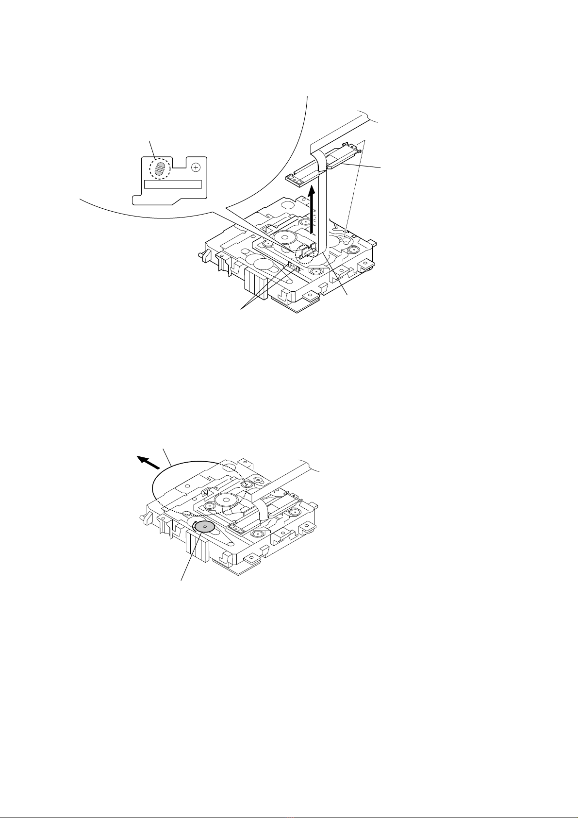
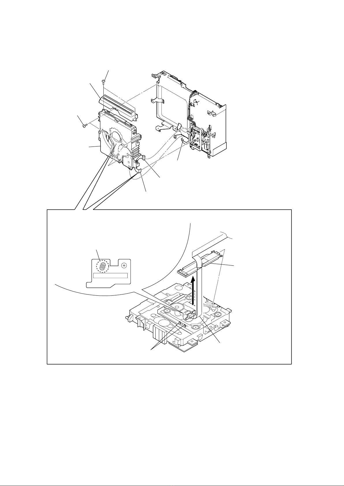
CD Mechanism Type CDM86 ASSY
Optical Pick-up Block Name KHM-313CAB
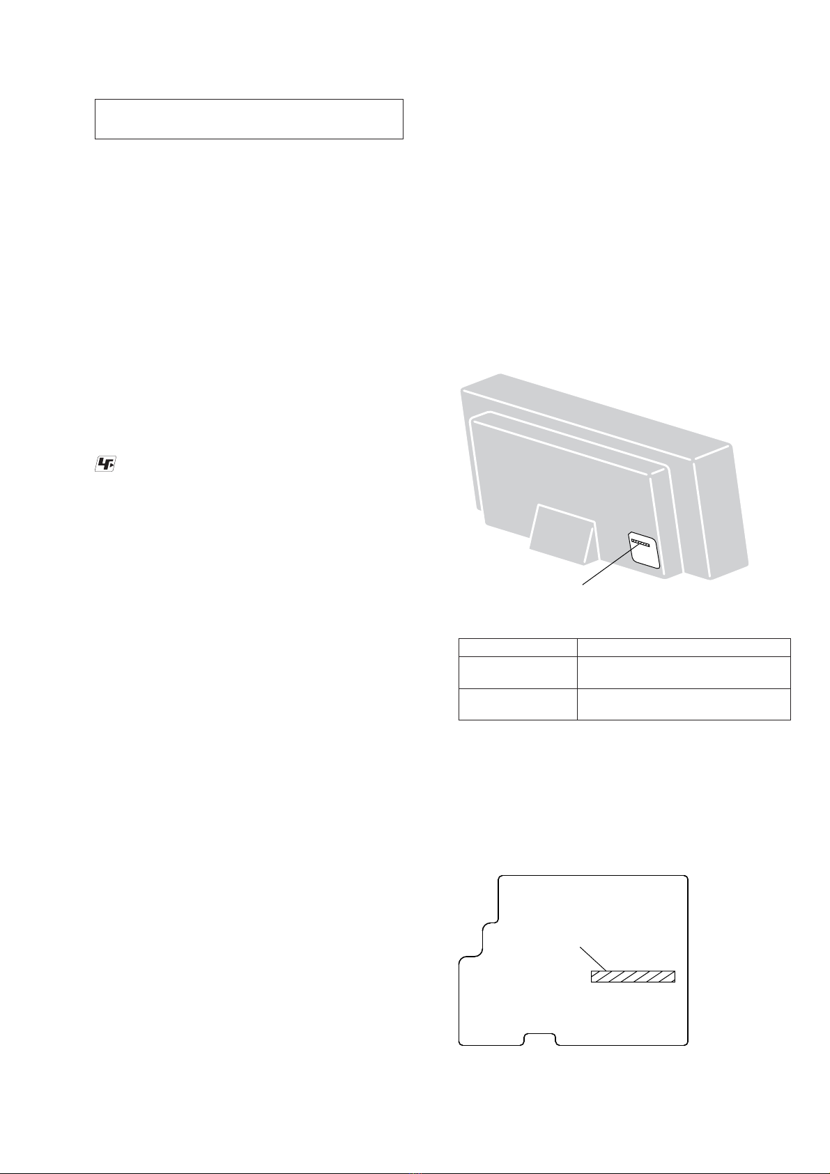
Photo: CMT-Z100iR
•iPod is a trademark of Apple Inc., registered in the U.S. and
other countries.
•MPEG Layer-3 audio coding technology and patents licensed
from Fraunhofer IIS and Thomson.
•Windows Media is a registered trademark of Microsoft Corpo-
ration in the United States and/or other countries.
Amplier section
Inputs
AUDIO IN (stereo mini jack):
Voltage 0.8 V, impedance 47 kilohms
Outputs
PHONES (stereo mini jack):
accepts headphones with an
impedance of 8 ohms or more
USB section
Supported bit rate:
MP3 (MPEG 1 Audio Layer-3):
32 320 kbps, VBR
WMA: 48 192 kbps
AAC: 48 320 kbps
Sampling frequencies:
MP3 (MPEG 1 Audio Layer-3):
32/44.1/48 kHz
WMA: 44.1 kHz
AAC: 44.1 kHz
(USB) port:
Maximum current:
500 mA
CD player section
System:
Compact disc and digital audio
system
Laser Diode Properties
Emission Duration: Continuous
Laser Output*: Less than 1000μW
* is output is the value measurement
at a distance of 200mm from the
objective lens surface on the Optical
Pick-up Block with 7mm aperture.
Frequency response: 20 Hz 20 kHz
Signal-to-noise ratio: More than 90 dB
Dynamic range: More than 90 dB
Tuner section
DAB tuner section (CMT-Z100DiR only):
Frequency range*
Band-III:
174.928 (5A) 239.200 (13F) MHz
* For details, see “DAB frequency table”
(page 48).
Antenna: DAB lead antenna
Antenna terminal: 75 ohms, F female
Speaker section
Speaker system:
2-way, bass-reex type
Speaker units:
Woofer: 100 mm, at type,
magnetically shielded
Tweeter: 20 mm, so dome type
Rated impedance: 8 ohms
General
Power consumption: 30 watts
Dimensions (w/h/d):
Approx. 535 × 220 × 198 mm
Mass: Approx. 5.7 kg
Supplied accessories:
Remote Commander (1), R3 (Size
AAA) batteries (2), FM lead antenna
(1), AM loop antenna (1), DAB lead
antenna (1) (CMT-Z100DiR only)
Design and specications are subject to
change without notice.
DAB frequency table (Band-III)
Frequency Label Frequency Label
174.928 MHz 5A 209.936 MHz 10A
176.640 MHz 5B 211.648 MHz 10B
178.352 MHz 5C 213.360 MHz 10C
180.064 MHz 5D 215.072 MHz 10D
181.936 MHz 6A 216.928 MHz 11A
183.648 MHz 6B 218.640 MHz 11B
185.360 MHz 6C 220.352 MHz 11C
187.072 MHz 6D 222.064 MHz 11D
188.928 MHz 7A 223.936 MHz 12A
190.640 MHz 7B 225.648 MHz 12B
192.352 MHz 7C 227.360 MHz 12C
194.064 MHz 7D 229.072 MHz 12D
195.936 MHz 8A 230.784 MHz 13A
197.648 MHz 8B 232.496 MHz 13B
199.360 MHz 8C 234.208 MHz 13C
201.072 MHz 8D 235.776 MHz 13D
202.928 MHz 9A 237.488 MHz 13E
204.640 MHz 9B 239.200 MHz 13F
206.352 MHz 9C
208.064 MHz 9D
* Frequencies are displayed to two decimal
places on this system.
FM stereo, FM/AM superheterodyne tuner
FM tuner section:
Tuning range:
87.5 108.0 MHz (50 kHz step)
Antenna: FM lead antenna
Intermediate frequency: 10.7 MHz
European model:
DIN power output (rated):
16 + 16 watts (8 ohms at 1 kHz, DIN)
Continuous RMS power output
(reference):
20 + 20 watts (8 ohms at 1 kHz,
10% THD)
Music power output (reference):
20 + 20 watts (8 ohms at 1 kHz,
10% THD)
Latin American model:
DIN power output (rated):
16 + 16 watts (8 ohms at 1 kHz, DIN)
Continuous RMS power output
(reference):
20 + 20 watts (8 ohms at 1 kHz,
10% THD)
Power requirements:
European model: 220 240 V AC,
50/60 Hz
Latin American model: 120 127 or
220 240 V AC, 50/60 Hz, adjustable
with voltage selector
AM tuner section:
Tuning range:
European model:
531 1,602 kHz (9 kHz step)
Latin American model:
530 1,710 kHz (10 kHz step)
531 1,710 kHz (9 kHz step)
Antenna: AM loop antenna
Intermediate frequency: 450 kHz

CMT-Z100DiR/Z100iR
2
1. SERVICING NOTES ............................................. 3
2. DISASSEMBLY
2-1. Disassembly Flow........................................................... 6
2-2. Panel (Back) Block ......................................................... 6
2-3. Plate (Back) Block .......................................................... 7
2-4. DAB Board (Z100DiR) .................................................. 7
2-5. Chassis Block.................................................................. 8
2-6. MAIN Board ................................................................... 9
2-7. CD Mechanism Deck (CDM86 ASSY) .......................... 10
2-8. Optical Pick-up Block (KHM-313CAB) ........................ 11
2-9. Display Block ................................................................. 11
2-10. HP Board, Tuner (FM/AM) ............................................ 12
2-11 Speaker Box (L/R) Block ............................................... 12
3. TEST MODE ............................................................ 13
4. ELECTRICAL CHECK ......................................... 13
5. DIAGRAMS
5-1. Block Diagram - CD, TUNER Section - ........................ 14
5-2. Block Diagram - MAIN Section -................................... 15
5-3. Block Diagram - POWER SUPPLY Section -................ 16
5-4. Printed Wiring Boards - CD Section - ............................ 18
5-5. Schematic Diagram - CD Section (1/3) -........................ 19
5-6. Schematic Diagram - CD Section (2/3) -........................ 20
5-7. Schematic Diagram - CD Section (3/3) -........................ 21
5-8. Printed Wiring Board - DAB Board (Z100DiR) - .......... 22
TABLE OF CONTENTS
NOTES ON CHIP COMPONENT REPLACEMENT
• Never reuse a disconnected chip component.
• Notice that the minus side of a tantalum capacitor may be dam-
aged by heat.
FLEXIBLE CIRCUIT BOARD REPAIRING
• Keep the temperature of soldering iron around 270 °C during
repairing.
• Do not touch the soldering iron on the same conductor of the
circuit board (within 3 times).
• Be careful not to apply force on the conductor when soldering
or unsoldering.
SAFETY-RELATED COMPONENT WARNING!
COMPONENTS IDENTIFIED BY MARK 0OR DOTTED LINE
WITH MARK 0ON THE SCHEMATIC DIAGRAMS AND IN
THE PARTS LIST ARE CRITICAL TO SAFE OPERATION.
REPLACE THESE COMPONENTS WITH SONY PARTS
WHOSE PART NUMBERS APPEAR AS SHOWN IN THIS
MANUAL OR IN SUPPLEMENTS PUBLISHED BY SONY.
5-9. Schematic Diagram - DAB Board (Z100DiR) - ............. 23
5-10. Printed Wiring Board - MAIN Section (1/2) -................ 24
5-11. Printed Wiring Boards - MAIN Section (2/2) - .............. 25
5-12. Schematic Diagram - MAIN Section (1/4) -................... 26
5-13. Schematic Diagram - MAIN Section (2/4) -................... 27
5-14. Schematic Diagram - MAIN Section (3/4) -................... 28
5-15. Schematic Diagram - MAIN Section (4/4) -................... 29
5-16. Printed Wiring Board - DISPLAY Board - ..................... 30
5-17. Schematic Diagram - DISPLAY Board -........................ 31
5-18. Printed Wiring Board - SUB DISPLAY Board - ............ 32
5-19. Schematic Diagram - SUB DISPLAY Board - ............... 33
5-20. Printed Wiring Boards - AUDIO IN/OUT, KEY,
DISPLAY POWER Section -.......................................... 34
5-21. Schematic Diagram - AUDIO IN/OUT, KEY,
DISPLAY POWER Section -.......................................... 35
6. EXPLODED VIEWS
6-1. Rear Cover Section ......................................................... 46
6-2. Front Panel Section......................................................... 47
6-3. Main Section ................................................................... 48
6-4. Display Section ............................................................... 49
6-5. Chassis Section ............................................................... 50
6-6. CD Mechanism Deck Section......................................... 51
7. ELECTRICAL PARTS LIST .............................. 52
Accessories are given in the last of the electrical parts list.
CAUTION
Use of controls or adjustments or performance of procedures
other than those specified herein may result in hazardous radia-
tion exposure.
This appliance is classified as a CLASS 1
LASER product. This marking is located on
the rear exterior.

CMT-Z100DiR/Z100iR
3
SECTION 1
SERVICING NOTES
NOTES ON HANDLING THE OPTICAL PICK-UP
BLOCK OR BASE UNIT
The laser diode in the optical pick-up block may suffer electro-
static break-down because of the potential difference generated by
the charged electrostatic load, etc. on clothing and the human body.
During repair, pay attention to electrostatic break-down and also
use the procedure in the printed matter which is included in the
repair parts.
The flexible board is easily damaged and should be handled with
care.
UNLEADED SOLDER
Boards requiring use of unleaded solder are printed with the lead-
free mark (LF) indicating the solder contains no lead.
(Caution: Some printed circuit boards may not come printed with
the lead free mark due to their particular size)
: LEAD FREE MARK
Unleaded solder has the following characteristics.
• Unleaded solder melts at a temperature about 40 °C higher
than ordinary solder.
Ordinary soldering irons can be used but the iron tip has to be
applied to the solder joint for a slightly longer time.
Soldering irons using a temperature regulator should be set to
about 350 °C.
Caution: The printed pattern (copper foil) may peel away if
the heated tip is applied for too long, so be careful!
• Strong viscosity
Unleaded solder is more viscous (sticky, less prone to flow)
than ordinary solder so use caution not to let solder bridges
occur such as on IC pins, etc.
• Usable with ordinary solder
It is best to use only unleaded solder but unleaded solder may
also be added to ordinary solder.
NOTE OF REPLACING THE IC102 ON THE DMB19C-
32NUA BOARD
IC102 on the DMB19C-32NUA board cannot exchange with
single. When this part is damaged, exchange the entire mounted
board.
NOTE OF REPLACING THE MS-214 BOARD
When the MS-214 board is damaged, exchange the entire MD
(AU) ASSY.
NOTE OF REPLACING THE TOUCH PANEL BOARD
When the TOUCH PANEL board is damaged, exchange the entire
PANEL (DISPLAY TOP) ASSY.
MODEL IDENTIFICATION
Model Power Voltage Indication
CMT-Z100DiR/CMT-
Z100iR: AEP model AC: 220-240V -50/60Hz 30W
CMT-Z100iR:
E2 model AC: 110-120/220-240V -50/60Hz 30W
NOTES ON LASER DIODE EMISSION CHECK
The laser beam on this model is concentrated so as to be focused
on the disc reflective surface by the objective lens in the optical
pickup block. Therefore, when checking the laser diode emission,
observe from more than 30 cm away from the objective lens. – Back Panel –
Power
Voltage
Indication
RELEASING THE DISC SLOT LOCK
The disc slot lock function for the antitheft of an demonstration
disc in the store is equipped.
Releasing Procedure:
1. Press [?/1] button to turn the power on.
2. Touch the [FUNCTION +] sensor to select CD function.
3. While touching the [x] sensor, press the [Z] button for more 5
seconds.
4. The message “UNLOCKED” is displayed and the disc slot is
unlocked.
Note: When “LOCKED”is displayed, the slot lock is not released by
turning power on/off with the [?/1]button.
• Abbreviation
E2 : Colombian, Venezuelan and Puerto Rican models
Ver. 1.1
IP BOARD DISCRIMINATION
In this set, the IP board has been changed in the midway of pro-
duction.
Repair after distinguishing each type set to doing the repair refer-
ring to the following.
– IP Board (Component Side) –
SUFFIX-12: 1-879-950-12
SUFFIX-21: 1-879-950-21

CMT-Z100DiR/Z100iR
4
HOW TO EJECT THE DISC WHEN POWER SWITCH TURNS OFF
Note: Please take out the CD mechanism block from a set.
PRECAUTION WHEN REMOVING OPTICAL PICK-UP BLOCK OR DMB19C-32NUA BOARD
CAUTION
2Lift up the FFC holder.
1two claws
3Be sure to execute a solder bridge as a measure against
static electricity when removing the OP block or
DMB19C-32NUA board. (Otherwise, the OP block will be
destroyed.)
– CD MECHANISM BLOCK Bottom view –
flexible flat cable
Please rotate the pully in the direction of the arrow after removing mechanism deck,
and eject the disc.
disc
– CD MECHANISM BLOCK Bottom view –

CMT-Z100DiR/Z100iR
5
MAIN BOARD SERVICE POSITION
• In checking the MAIN board, prepare extension jig (Part No. J-2501-102-A: 1.00 mm pitch, 13 cores, length 300 mm).
Note: Pleaese connect it after taking out MAIN board, DMB19C-32NUA board and CD mechanism block of the set referring to Section 2 Disassembly
(page 6)
MAIN board
DMB19C-32NUA board
CD mechanism block
Connect extension jig (J-2501-102-A) to
the MAIN board (CN861) and
DMB19C-32NUA board (CN109).
HP board

CMT-Z100DiR/Z100iR
6
SECTION 2
DISASSEMBLY
• This set can be disassembled in the order shown below.
2-1. DISASSEMBLY FLOW
Note: Follow the disassembly procedure in the numerical order given.
2-2. PANEL (BACK) BLOCK
Note: This illustration sees the set from rear side.
2-2. PANEL (BACK) BLOCK
(Page 6)
2-3. PLATE (BACK) BLOCK
(Page 7)
2-4. DAB BOARD (Z100DiR)
(Page 7)
2-10. HP BOARD, TUNER (FM/AM)
(Page 12)
2-11. SPEAKER BOX (L/R) BLOCK
(Page 12)
2-5. CHASSIS BLOCK
(Page 8)
2-6. MAIN BOARD
(Page 9)
2-7. CD MECHANISM DECK (CDM86 ASSY)
(Page 10)
2-9. DISPLAY BLOCK
(Page 11)
SET
2-8. OPTICAL PICK-UP BLOCK (KHM-313CAB)
(Page 11)
1screw (BVTP3 u10)
3two screws (B4 u10)
2lid (cord) block
4panel (stand) block 5three screws (BVTP3 u10)
5three screws
(BVTP3 u10)
5two screws
(BVTP3 u10)
5three screws (BVTP3 u10)
6panel (back) block

CMT-Z100DiR/Z100iR
7
2-3. PLATE (BACK) BLOCK
Note: This illustration sees the set from rear side.
2-4. DAB BOARD (Z100DiR)
Note: This illustration sees the set from rear side.
1screw (BVTP3 u10)
2coating clip
1ten screws (BVTP3 u10)
1two screws (BVTP3 u10)
1two screws (BVTP3 u10) 1six screws (BVTP3 u10)
3plate (back) block
3two screws (BVTP3 u10)
9DAB board
CAUTION
The number and the width of the pins are the
same as CN840 and CN850.
Take care not to insert the flexible flat cable
(11 core) by mistake.
CN840
MAIN board
CN850
1flexible flat cable (11 core)
(CN850)
4screw
(BVTP2.6)
5module (DAB tuner)
6two screws
(BVTP2.6)
7bracket (DAB)
8flexible flat cable (11 core)
(CN801)
2connector

CMT-Z100DiR/Z100iR
8
2-5. CHASSIS BLOCK
Note: This illustration sees the set from rear side.
qs five screws
(BVTP3 u8)
1Cut the wire holder. 2power cord connector
(CN01)
3connector
(CN820)
4two speaker connectors
(CN390, CN391)
7connector
(CN880)
8flexible flat cable (11 core)
(CN870)
9connector
(CN880)
0flexible flat cable (7 core)
(CN811)
qa flexible flat cable (9 core)
(CN810)
qd chassis block
5connector
(CN350)
6flexible flat cable (9 core)
(CN830) (Z100iR: E2)/
flexible flat cable (11 core)
(CN840) (Z100DiR/Z100iR: AEP)
CAUTION
The number and the width of the pins are the
same as CN840 (Z100DiR/Z100iR: AEP) and
CN850.
Take care not to insert the flexible flat cable
(11 core) (Z100DiR/Z100iR: AEP) by mistake.
CN840 (Z100DiR/Z100iR: AEP)
MAIN board
CN850
• Abbreviation
E2 : Colombian, Venezuelan and
Puerto Rican models

CMT-Z100DiR/Z100iR
9
2-6. MAIN BOARD
Note: This illustration sees the set from rear side.
CAUTION
The number and the width of the pins are the
same as CN811 and CN860.
Take care not to insert the flexible flat cable
(7 core) by mistake.
CN860
MAIN board
CN811
1connector
(CN601)
2flexible flat cable
(13 core) (CN861)
3six screws (BVTP3 u8)
4harness
3screw (BVTP3 u8)
5flexible flat cable
(7 core) (CN860)
6screw
(BVTP2.6)
7heat sink (AMP)
8radiation sheet
qa MAIN board
9connector
(CN02)
(Z100iR: E2)
0SW-VOLT board
• Abbreviation
E2 : Colombian, Venezuelan and
Puerto Rican models

CMT-Z100DiR/Z100iR
10
2-7. CD MECHANISM DECK (CDM86 ASSY)
Note: This illustration sees the set from rear side.
CAUTION
5Lift up the FFC holder.
flexible flat cable
4two claws
6Be sure to execute a solder bridge as a measure against
static electricity when removing the OP block or
DMB19C-32NUA board.
(Otherwise, the OP block will be destroyed.)
1flexible flat cable (7 core)
(CN001)
2connector
(CN201)
3three screws (BVTP3 u8)
7wire (flat type) (24 core)
(CN101)
8two screws (BVTP2.6)
9panel (slot) block
0CD mechanism deck
(CDM86 assy)

CMT-Z100DiR/Z100iR
11
2-8. OPTICAL PICK-UP BLOCK (KHM-313CAB)
2-9. DISPLAY BLOCK
Note: This illustration sees the set from rear side.
4two insulator screws
4two insulator screws 5two insulators
6wire
5two insulators
7optical pick-up block
(KHM-313CAB)
1two claws
2FFC holder
3wire (flat type) (24 core)
3eight screws (BVTP2.6)
2ferrite core
1cushion (ferrite)
4display block

CMT-Z100DiR/Z100iR
12
2-10. HP BOARD, TUNER (FM/AM)
Note: This illustration sees the set from rear side.
2-11. SPEAKER BOX (L/R) BLOCK
Note: This illustration sees the set from rear side.
2screw (BVTP3 u10)
1connector
(CN350)
(Z100DiR)
3HP board
6cushion (FFC5P)
4connector
5screw (BVTP3 u10)
8two screws (BVTP3 u10)
9bracket (antenna) block
qa tuner (FM/AM)
0cushion (tuner)
0two cushions (tuner)
7flexible flat cable (9 core) (Z100iR: E2)/
flexible flat cable (11 core) (Z100DiR/Z100iR: AEP)
1screw
(BVTP3 u10)
5SW-VOLT board
Arrangement of power cord
power cord ferrite core
2CORD HOLDER
board
3power cord (with ferrite core)
4two screws
(BVTP3 u10)
(Z100iR: E2)
A
B
A
B
6two speaker connectors
(CN390, CN391)
7two cushions (ferrite)
8clamp filter
9speaker box (L) block
9speaker box (R) block
• Abbreviation
E2 : Colombian, Venezuelan and
Puerto Rican models
• Abbreviation
E2 : Colombian, Venezuelan and
Puerto Rican models
Ver. 1.1

CMT-Z100DiR/Z100iR
CMT-Z100DiR/Z100iR
1313
SECTION 3
TEST MODE
SECTION 4
ELECTRICAL CHECK
COLD RESET
The cold reset clears all data including preset data stored in the
memory to initial conditions. Execute this mode when returning
the set to the customer.
Procedure:
1. Press the [?/1] button to turn the power on.
2. Press two buttons of [DSGX] and [?/1] simultaneously for
more 3 seconds.
3. The set enters standby status.
PANEL TEST MODE
Enter The Panel Test Mode
Procedure:
1. Press the [?/1] button to turn the power on.
2. While pressing the [u] sensor, press the [DISPLAY] button
for more 3 seconds.
3. When the panel test mode is activated, segments of the fluores-
cent indicator tube and sub display are all turned on.
Version Check
Procedure:
1. In the panel test mode, touch the [ENTER] sensor.
2. On the fluorescent indicator tube, model name and destination
are displayed.
3. Each time the [ENTER] sensor is touched, the display changes
starting from MC, GC, USBL, USBM, IPL, CD, CDD, CDMA,
CDMB, BDA, BDB, ST, TA and TM version this order, and
returns to the MC version display.
In this state, each time the [x] sensor is touched, the version
and date are switched.
4. To release from this mode, while pressing the [u] sensor,
press the [DISPLAY] button for more 3 seconds.
Key Test Mode
Procedure:
1. In the panel test mode, press the [DSGX] button.
2. The message “K0” displayed. Whenever any buttons are
pressed and the any sensors are touched, the value is changed.
3. To release from this mode, while pressing the [u] sensor,
press the [DISPLAY] button for more 3 seconds.
Key Address Monitor Mode
Procedure:
1. In the panel test mode, touch the [VOLUME +] sensor.
2. Enter the key address monitor mode.
3. In this state, whenever either of button is pressed, the address
corresponding to each button is displayed on the sub display.
4. To release from this mode, while pressing the [u] sensor,
press the [DISPLAY] button for more 3 seconds.
CD SHIP MODE
This mode can run the CD sled motor optionally. Use this mode,
for instance, when cleaning the optical pick-up.
Procedure:
1. Press the [?/1] button to turn the power on.
2. Confirm there is no disc in disc slot.
3. Touch the [FUNCTION +] sensor to select CD function.
4. While touching the [x] sensor, press the [?/1] button.
5. Set to the CD ship mode (chucking on).
FM TUNE LEVEL CHECK
signal
generator
set
Procedure:
1. Turn on the set.
2. Input the following signal from signal generator to FM antenna
input directly.
Carrier frequency : A = 87.5 MHz, B = 98 MHz, C = 108 MHz
Deviation : 75 kHz
Modulation : 1 kHz
ANT input : 35 dBu (EMF)
Note: Use 75 ohm coaxial cable to connect signal generator and the set.
You cannot use video cable for checking.
Use signal generator whose output impedance is 75 ohm.
3. Set to FM tuner function and tune A, B and C signals.
4. Confirm “TUNED” is lit on the display for A, B and C signals.
When the selected station signal is received in good condition,
“TUNED” is displayed.
TUNER SECTION
CD SHIP & MEMORY CLEAR MODE
Procedure:
1. Press the [?/1] button to turn the power on.
2. Confirm there is no disc in disc slot.
3. Touch the [FUNCTION +] sensor to select CD function.
4. While touching the [x] sensor, press the [DSGX] button for
more 3 seconds.
5. Set to CD ship mode (chucking on), and the memory is cleared.
CD SLOT LOCK
This mode is for the antitheft of CD disc in shop (not for transport).
Procedure:
1. Press the [?/1] button to turn the power on.
2. Touch the [FUNCTION +] sensor to select CD function.
3. Insert a disc.
4. While touching the [x] sensor, press the [Z] button for more 5
seconds.
5. The message “LOCKED” is displayed and the disc slot is
locked (Even if exiting from this mode, the disc slot is still
locked).
6. If press the [Z] button to eject the disc, the message “LOCKED”
is displayed and can not eject the disc.
7. To release this lock, while touching the [x] sensor, press the
[Z] button for 5 seconds again.
8. The message “UNLOCKED” is displayed and the disc slot is
unlocked.
CHANGE-OVER THE AM TUNING INTERVAL
(Z100iR: Colombian, Venezuelan and Puerto Rican
models)
The AM tuning interval can be changed over 9 kHz or 10 kHz.
Procedure:
1. Press the [?/1] button to turn the power on.
2. Touch the [FUNCTION +] button to select AM function.
3. Press the [?/1] button again to turn the power off (standby).
4. After pressing the [DISPLAY] button, while touching the
[FUNCTION +] sensor, press the [?/1] button.
5. It turns power on and thus the tuning interval is changed over.
COMMON TEST MODE
Procedure:
1. Press the [?/1] button to turn the power on.
2. While touching the [u] sensor, press the [DSGX] button for
more 3 seconds.
3. It enters the common test mode and the “PLAY SLEEP” seg-
ment on the fluorescent indicator tube blinks.
4. Each time the [VOLUME +]/[VOLUME –] sensors are
touched, “VOLUME MIN” and “VOLUME MAX” are dis-
played.
5. Each time the [EQ] button on the remote commander is
pressed, “TONE MAX”, “TONE MIN” and “TONE FLAT”
are displayed.
6. To release from this mode, press the [?/1] button to turn the
power off.
TOUCH PANEL BEEP ON/OFF SETTING MODE
Procedure:
1. Press the [?/1] button to turn the power on.
2. While touching the [x] sensor, press the [DISPLAY MODE]
button for 5 seconds.
3. Display “BEEP OFF” or “BEEP ON”, and thus the beep on/off
setting is changed over.

CMT-Z100DiR/Z100iR
CMT-Z100DiR/Z100iR
1414
SECTION 5
DIAGRAMS
5-1. BLOCK DIAGRAM - CD, TUNER Section -
OPTICAL PICK-UP
BLOCK
RF AMP, SERVO DSP,
AUDIO PROCESSOR
IC101
SYSTEM
CONTROLLER
IC801 (1/3)
FOCUS/TRACKING COIL DRIVE,
SPINDLE/SLED MOTOR DRIVE
IC201
AUTOMATIC POWER
CONTROL
Q102-1
RF_IP
125
RF_C
3
RF_B
2
RF_A
1
RF_D
4
RF
VOA/A
VOB/B
VOC/C
VOD/D
RF_F6VOE/E+G
RF_E5VOF/F+H
V2O12VC
LDO117LD (780)
AUTOMATIC POWER
CONTROL
Q102-2
LDO2
18LD (650)
FOO25
CD ON
SWITCH
Q101-1
CD ON
SWITCH
Q101-2
VR (780)
MSW
GPIO
23
118
VR (650)
FCS+
MSW
MDI115
MDI216
PD
LIMIT
Q103
SF_CS# CS_
SD-RAM
IC104
X101
27MHz
36
FCS– 37 1
TRO24
TRK+ 35
TRK– 34 4
FMO21
SL+ 29
SL– 30 10
DMO20
SP+ 27
SP– 28
31
32
41
46
47
13
SPFG/OPINN12845
GPIO
GPIO
GPIO
120
DG0, DQ1 – DQ15
RD0 – RD15
A0 – A11
RA0 – RA11
2, 4, 5, 7, 8, 10, 11, 13, 42,
44, 45, 47, 48, 50, 51, 53
45 – 49, 51 – 53,
64 – 61, 56 – 59
82, 83, 85, 86,
74 – 69, 81, 67
23 – 26,
29 – 34, 22, 35
36
XTALI 9
1
SF_CK SCK
39 6
BA0 BA0
78
20
BA1 BA1
80
21
RCLK CLK
66
38
DQM0 LDQM
55
15
DQM1 UDQM
65
39
RAS# RAS
77
18
CAS# CAS
76
17
RWE# WE
75
16
: CD PLAY
: TUNER
: DAB
: USB
FOCUS
COIL DRIVE
TRACKING
COIL DRIVE
SLED
MOTOR DRIVE
SPINDLE
MOTOR DRIVE
LODING
MOTOR DRIVE
REGULATOR
GPIOMUTE123 11619
MUTE4MUTE4 2220
GPIOTSD-M 9422
IOPMON/
OPINP
12740
8
PS 21
BUFFER
BUFFER
RF +3.3V
43
PRST#
REGO2
REGO1
MS-214
BOARD
(KHM-313CAB)
FLASH ROM
IC102
XTALO 10
L-OUT
115
119
GPIO
114
GPIO19 106
VINL
14
13
VINR
BCK
7
LRCK
6
8
SCKI
A/D CONVERTER
IC4601
9DOUT
R-CH
AOUT-L
5
8
AOUT-R
D/A CONVERTER
IC4602
1SDATA
2SCLK
3LRCK
4MCLK
USB_DP 27
R-CH
USB_DM 28
SO
2
SI
5
SF_DO 37
SF_DI 38
CN901
(USB)
3
2
O_XSYSRST50
O_CD-SOD
31
I_CD-SDI
32
O_CD-SCK
33
O_XIFCS
52
I_XIBSY
51
O_REV
44
O_FWD
45
IFSDI 35
IFSOD 41
IFSCK 40
IFCS# 88
IFBSY 87
I_TRG-SW39
I_CKSW1
42
I_OCSW1
43
SIGNAL PATH
R-ch is omitted due to same as L-ch.
OPOUT126
25
24
16
17
TUNER (FM/AM)
AM
FM ANT
AM ANT
L-OUT
R-OUT
DO/STEREO
R-CH
DI
CLK
CE
FM 75 :
COAXIAL
57 I_ST DATA IN/STEREO
TUNED 60 I_TUNED
RDS INT 18 I_RDS-INT
RDS DATA 7I_RDS DATA
59 I_ST DATA OUT
58 O_ST CLK
56
DAB TUNER MODULE
AUDL
AUDR
S1_DIN
R-CH
S1_DOUT
DAB 75 :
35
36
O-ST CE
O_DAB TxD_OUT
I_DAB RxD_IN
LINE
AMP
IC803
A
REC-L B
TUNER-L C
DAB-L D
(Z100DiR)
(Z100DiR/Z100iR: AEP)
(Page 15)
(Page 15)
(Page 15)
(Page 15)

CMT-Z100DiR/Z100iR
CMT-Z100DiR/Z100iR
1515
: TUNER
: AUDIO IN
: DAB
SIGNAL PATH
: iPod
1 IN-L1 23OUT L
26
SDA
25
SCL
11VOL L
VOL IIC_SDA/E2P-SDA
24
O_HP MUTE
21
VOL IIC_CLK/E2P-SCL
22
O_SEL A
1
O_SEL INH
5
MUTING
CONTROL
Q353, 354, 356
O_XHP LINE MUTE
25
MUTING
CONTROL
Q357
MUTING
Q355
10SEL L
INPUT SELECT,
ELECTRICAL VOLUME
IC301
AUDIO SELECT
IC320
SYSTEM CONTROLLER
IC801 (2/3)
J310 R-CH
R-CH
AUDIO IN
J350
R-CH
PHONES
L-OUT
R-ch is omitted due to same as L-ch.
LINE
AMP
IC340
LINE
AMP
IC360
A
SHUTDOWN E
REC-L
B
TUNER-L
C
DAB-L
D
(Z100DiR)
(Z100iR)
3IN-L2
5IN-L3
12 13X0 X
14 X1
Q321Q320
10 6
AINH
CN951
(iPod Dock)
19
30
18
RXD
TXD
DGND
27
LINE-OUT-L 28
LINE-OUT-R
7IN-L4
77 O_iPod_TxD_OUT
78 I_iPod_RxD_IN
73 II_iPod DET
EEPROM
IC855
HEADPHONE
AMP
IC350
I_HP DET
6
R-CH
R-CH
PROTECT
DETECT
Q392
OVER LOAD
DETECT
Q190, 191
SP391
(L-ch)
SP390
(R-ch)
5
SHUTDOWN
LINP
21LOUTN
19
20
22
LOUTP
LOUTP
LOUTN
4644
FAULT
POWER AMP
IC380
26O_BUZZER BZ991
(BUZZER)
MUTE
45
SHUTDOWN
SWITCH
Q394
PROTECT
DETECT
Q390
O_DAMP_SHUTDOWN
27
O_TA LINE-MUTE
23
I_XDAMP_PROTECT
28
ND621
FLUORESCENT
INDICATOR TUBE
FLUORESCENT INDICATOR
TUBE DRIVER
IC621
AD2, AD1,
SG1 - SG35
37
59 - 64, 1 - 31
DIN O_MAIN FL SD
55
CLKB O_MAIN FL SCLK
54
CSB O_MAIN FL CS
53
91 92 90
RSTB O_MAIN FL RESET
52
89
TP SDA
TP SCL
I_TP TINT
47 48 75
I_SIRCS
4
O_TP RESET
49
32
S661 - 665
(PANEL KEYS)
100
O_STBY LED
D661
STANDBY
GR2 - GR11
GR1
33 - 42
10 GRID DRIVE
Q621
D50 - 96,
(for BLACK model)
D420 - 428, 431 - 468
(for WHITE model)
(SUB DISPLAY)
SUB DISPLAY
CONTROLLER
IC420
SG1 - SG11
11
14 - 24
DIN O_SUB DISP SD
7
CLK O_SUB DISP SCLK
8
STB O_SUB DISP STB
9
95 94 93
I_KEY WAKE UP_POWER
D802
74
GR1 - GR5
42 - 38
5
I_KEY1, I_KEY2
83, 82
2
LED DRIVE
Q420 - 440
LED DRIVE
Q661
TOUCH
PANEL
BOARD
REMOTE
CONTROL
RECEIVER
IC622
X801
32.768kHz
Xcout
Xcin
11 10
X802
5MHz
Xout
Xin
13 15
LINE
AMP
IC330
5-2. BLOCK DIAGRAM - MAIN Section -
(Page 14)
(Page 14)
(Page 14)
(Page 14)
(Page 16)

CMT-Z100DiR/Z100iR
CMT-Z100DiR/Z100iR
1616
POWER CONTROL
IC01
D16
D507
D804, 805
D42
+3.3V
(AC IN)
F01
LINE FILTER
L001,
(Z100DiR/Z100iR: AEP)
L002
(Z100iR: E2)
VOLTAGE
SELECTOR
S001
RECT
D01
TH01
SYSTEM CONTROLLER
IC801 (3/3)
15 VS
18 VD
1 VSENSE
2 F/B
16 VG (H)
12 VG (L)
8VC1
POWER CONTROL
IC02
5 DRAIN
2FB
4VCC
ISOLATOR
PH501
ISOLATOR
PH502
ISOLATOR
PC401
T20
MAIN POWER
TRANSFORMER
T001
SUB POWER
TRANSFORMER
RECT
D801
SWITCHING
Q11
SWITCHING
Q12
SHUNT
REGULATOR
IC555
RECT
D501
Q10
9OCP
D503
D405
+11V
(Z100iR: E2)
+9V
LED +6V
AMP B+
+9V
REGULATOR
IC552
+6V
REGULATOR
IC554
RECT
D502
DAB +3.3V
DAB +1.2V
+3.3V
REGULATOR
IC801
AVDD +5V
+1.2V
REGULATOR
IC802
AVDD +1.8V
+1.8V
REGULATOR
IC111
(Z100DiR)
D +5V
DVDD +3.3V
+5V
REGULATOR
IC551
+3.3V
REGULATOR
IC553
AUDIO +9V
+9V
REGULATOR
IC590
USB +5V B+ SWITCH
IC550
iPod +5V B+ SWITCH
IC853
RF +3.3V
+3.3V
REGULATOR
IC107
DC DETECT
Q402, 403
D563
D562
D570
D564
D561
D590
POWER
ON/OFF
CONTROL
SWITCH
Q401
+5V
REGULATOR
IC591
T621
DC/DC CONVERTER
TRNASFORMER
RECT
D621, 622
OSC
Q622
VEE
AC 4.0V
D566
Q530
D530
D832
SHUTDOWN
SWITCH
Q830
PROTECT
DETECT
Q821
SHUTDOWN E
I_AC-CUT 20
I_RESET 12
O_POWER ON 87
I_AC DET 85
I_POWER_PROTECT 84
O_DAB-POWER_1.2 37
O_DAB-POWER_3.3 38
O_USB POWER 65
I_XUSB PROTECT 67
O_iPod POWER 79
iPod PROTECT 72
RESET SIGNAL
GENERATOR
IC850
RESET SWITCH
Q851
xAbbreviation
E2 : Colombian, Venezuelan and Puerto Rican models
5-3. BLOCK DIAGRAM - POWER SUPPLY Section -
(Page 15)

CMT-Z100DiR/Z100iR
CMT-Z100DiR/Z100iR
1717
• Circuit Boards Location
For Schematic Diagrams.
Note:
• All capacitors are in μF unless otherwise noted. (p: pF) 50
WV or less are not indicated except for electrolytics and
tantalums.
• All resistors are in Ωand 1/4 W or less unless otherwise
specified.
• f: Internal component.
• 2: Nonflammable resistor.
• C: Panel designation.
THIS NOTE IS COMMON FOR PRINTED WIRING BOARDS AND SCHEMATIC DIAGRAMS.
(In addition to this, the necessary note is printed in each block.)
• A: B+ Line.
• B: B– Line.
• Voltages and waveforms are dc with respect to ground
under no-signal (detuned) conditions.
no mark
: TUNER (FM/AM)
( ): CD PLAY
< >: DAB
*: Impossible to measure
• Voltages are taken with VOM (Input impedance 10 MΩ).
Voltage variations may be noted due to normal production
tolerances.
• Waveforms are taken with a oscilloscope.
Voltage variations may be noted due to normal production
tolerances.
• Circled numbers refer to waveforms.
• Signal path.
F: TUNER
J: CD PLAY
L: DAB
g: iPod
E: USB
f: AUDIO IN
• Abbreviation
E2 : Colombian, Venezuelan and
Puerto Rican models
For Printed Wiring Boards.
Note:
• X: Parts extracted from the component side.
• Y: Parts extracted from the conductor side.
• f: Internal component.
• : Pattern from the side which enables seeing.
(The other layers’ patterns are not indicated.)
• Indication of transistor.
C
B
These are omitted.
E
Q
CEB
These are omitted.
Caution:
Pattern face side:
(SIDE B)
Parts face side:
(SIDE A)
Parts on the pattern face side seen
from the pattern face are indicated.
Parts on the parts face side seen from
the parts face are indicated.
Note: The components identified by mark 0or dotted
line with mark 0are critical for safety.
Replace only with part number specified.
Caution:
Pattern face side:
(Conductor Side)
Parts face side:
(Component Side)
Parts on the pattern face side seen
from the pattern face are indicated.
Parts on the parts face side seen from
the parts face are indicated.
• DMB19C-32NUA board is multi-layer printed board.
However, the patterns of intermediate layers have not
been included in diagrams.
HP board
POWER KEY board
TUNER (FM/AM)
DAB board
(Z100DiR)
USB board
IP board
DISPLAY board
DISPLAY POWER board
TOUCH PANEL board
DMB19C-32NUA boar
d
SW-VOLT board
(Z100iR: E2)
SUB DISPLAY board
TOP KEY board
MS-214 board
MAIN board
MODULE (DAB TUNER)
(Z100DiR)
• Abbreviation
E2 : Colombian, Venezuelan and
Puerto Rican models
• Abbreviation
E2 : Colombian, Venezuelan and
Puerto Rican models

CMT-Z100DiR/Z100iR
CMT-Z100DiR/Z100iR
1818
1
719
113
C1504
CN201
R1110
CN4602
R230
R1114
R231
R232
CN601
R1121
R1123
C4608
R246
R247
JL001
JL002
JL003
JL004
JL005
JL006
C216
JL007
C217
C218
CL105
CL106
C602
CL107
C603
CL108
C604
CL109
JL201
JL202
JL203
JL010
C220 JL205
JL012
JL206
JL014
R4601 JL016
JL017
C611
JL210
JL211
JL212
JL213
JL214
JL215
R1151
R1152
C620
R622
R623
FB1264
FB1265
FB1266
R1168
R4837 R4838
RB105 RB106
ET002
RB107
ET003
RB108
ET004
RB111
RB112
RB113
RB114
RB115
JL1201
JL1202
JL1203
JL1204
JL1205JL1206 JL1207
JL1208
JL1209
JL1210
JL1211
JL1212
JL1213
JL1214
JL1216
JL1218
JL1220
R102
R103
R107
R114
CN101
CN105
C101
C105
R142
C106
X101
C112
C113
C118
R156
C124
CL206
CL207
CL208
JL113
JL114
JL115
CL213
R1248
R1249
R1263
C152
C153
R1269
C160
R1276
R1277
R1281
R1282
R1283
IC101
IC104
JL1101
JL1102
JL1105
JL1106
JL1107 JL1108
C190
JL1110
JL1111
JL1112
JL1113
JL1114
JL1115
JL1116
JL1117
CL1138
JL1118
CL1139
JL1119
CL1140
JL1120
CL1141
JL1121
CL1142
JL1122
JL1123
JL1124
CL1146
CL1147
CL1148
CL1149
CN1105
CL1150
CL1151
JL1131
CL1152
JL1132 JL1133
JL1134
1
12
13
48
24
25
3637
IO
C1
E1
B1
B2
E2
C2
D1
G2
S2
G1
D2
S1
FB607
R210
C1505
R212
C1506
R213
C1507
R214
R215 R216
R219 R1101
C1512
C1513
R220
FB608
R221
R223
R224
R225
R226
R233
R234
C4602
C4603
C4606
C203
C205
C206
C208
R1129
C209
C210
C211
C212
C213
C214
C215
C219
R256
C4622
C4623
C221
C4626
C222
C224
R4602 R4605
R4606
R4608
R4609
IC4601
IC4602
R1150
C233 R4611
FB1267
FB1268
R1177
R1178
D005
Q101
Q102
Q103
R4833
R1184
R4834
R4835
R1191
R1192
R1193
R1194
IC201
R1251
R101
R108
R109
R110
R111
R112
R113
R115
R116
R117
R118
R120
R121
R122
R123
R124
R125
R133
R136
R521
C102
C108
C111
C115
C116
C119
C502
CL201
CL202
CL204
C125
CL205
C126
C127
FB106
R1252
R1255
R1256
C144
C145
C146
C149
R1261
R1262
C150
C151
C154
C155
C156
R1278
R1279
C168
C169 R1280
C172
C175
C179
C180
C181
IC102
C183
IC107
C188
C191
IC111
C192
C193
C195
C197
C198
C199
FL603
R204
R205
R206
R207
R208
R209
FB603
CN109
FB606
A
B
C
D
E
1 2 3 4 5 6 7 8 9 10 11 12
1
32
1
6
1
27
54
28
96
97 128
64 33
65
6
1
23
1
24
2
41
NMAIN BOARD
CN860 LMAIN BOARD
CN501
KUSB BOARD
CN993
MMAIN BOARD
CN861
1-878-221-
12
(12)
DMB19C-32NUA BOARD (SIDE A)
OPTICAL
PICK-UP
BLOCK
(KHM-313CAB)
MS-214
BOARD
(NC)
(CHASSIS)
(CHASSIS)(CHASSIS)
1-878-221-
12
(12)
DMB19C-32NUA BOARD (SIDE B)
13
45
18
45
1
14
7
8
1
8
4
5
1
8
4
5
K
A/K
A
E
C1515
C1516
1
7
CN202
R192
R195
R197
R198
R236
R238
R239
R255
C223
C225
C226
R2502
R2505
R227
R228
R254
R2507
FB609
C601
C607
C610
C630
C640
C641
R2506
R237
(NC)
Note 1: IC102 on the DMB19C-32NUA board cannot exchange with single.
When this part is damaged, exchange the entire mounted board.
Note 2: When the MS-214 board is damaged, exchange the en-
tire MD (AU) ASSY.
5-4. PRINTED WIRING BOARDS - CD Section - • : Uses unleaded solder.
• See page 17 for Circuit Boards Location.
(Page 25) (Page 34)
(Page 25) (Page 25)

CMT-Z100DiR/Z100iR
CMT-Z100DiR/Z100iR
1919
(2/4)
MAIN
BOARD
M
CN861
CN993
USB
BOARD
K
BOARD
(2/3)
6
DMB19C-32NUA
5
(3/3)
DMB19C-32NUA
BOARD
(2/3)
BOARD
DMB19C-32NUA
1
IC B/D
IC B/D
4
(3/3)
DMB19C-32NUA
BOARD
(2/3)
DMB19C-32NUA
3
BOARD
(2/3)
DMB19C-32NUA
2
BOARD
1
2
3
4
(2/3)
DMB19C-32NUA
9
BOARD
0.4 (0.1) 0.4 (2)
3.7 (3.2)3.7
3.3 (2.6)3.3
0.1
5
0.1
0.1
0.1
0.1
5
0.1
3.3
1.3
5
3.3
3.3
3.3
0.6
1.8
0.4
1.3
3.3
3.3
1
0.2
3.3
1.5
1.5
1.4
1.5 (1.1)
0.1
0.1
0.1
3.1
1.6
2
3.3
2
1.5
1.3 (2.2)
1.3 (2.2)
0.6
0.1
1.2
0
3
2.8
3.1
2
3.3
1.3 ()
0.5 ()
0.6 ()
0.9 ()
1.3 ()
1 ()
1 ()
3.3
3.3
3.3
1.4 ()
1.5 ()
3.3
3.3
1.8 ()
1.1 ()
1.3 ()
2 ()
1.5 ()
1.9 ()
0.6 ()
0
3.3
3.1
0.1
3.3
3.3
1.8
3
2.5
1.5
1.3 (2.2)
1.3 (2.2)
3.3
0.6
0.1
2
1.2
3
2.8
3.1
1.5
1.5
1.4
1.5 (1.1)
0.1
0.1
0.1
3.3
1.6
2
1.3
3.3
3.3
1.2
0.1
0
0
0
0
0.1
3.3
3.3
1
1.7
3.3
1.7
1.6
0.1
1.7
1
3.3
3.3
1.8
1.1
1.1
1.5
2.7
2
2
2
2
2
2
1.8
3.3
0.9
0.6
2
1.5
0.7
0.1
0.1
3.3 (2.6)
3.3
3.3
1.5
1.5
3.3
0.1
1.5
1.5
3.3
2.9
0.1
3.3
0.8
1.8
1
3.3
0.4
1.3
0.2
3.1
0.1
3.3
1.4 ()
1 ()
1 ()
1.3 ()
0.9 ()
3.3
0.6 ()
0.5 ()
1.3 ()
1.8
2
0.6 ()
1.9 ()
1.5 ()
2 ()
1.3 ()
1.1 ()
1.8 ()
1.5 ()
1
2
3
4
5
6
6P
CN105
TXD
RXD
GND
+3.3V
V2REFO
RFMON
47k
R124
3.3k
R1151
0.01
C192
0.1
C179
100
R156
22
R112
2.7kR111 0
100k
R114
0.1
C116
100
R109
0.01
C113
22R115
100
R101
10k
R107
10V
47
C105
0.22
C195
47k
R117
1k
R116
1
C124
3.3k
R1150
0.01
C101
22
R121
0.1C115
10V
47
C112
1M
R108
1
2
3
4
5
6
7
8
9
10
11
12
13
14
15
16
17
18
19
20
21
22
23
24
CN101
24P
GND (LD)
LD (650)
NC
NC
PD
LD (780)
VR (650)
VR (780)
NC
VOE/E+G
VCC
VC
GND (PDIC)
VOF/F+H
VOB/B
VOA/A
RF
(LO:DVD.HI:CD)MSW
VOD/D
VOC/C
TRK-
TRK+
FCS+
FCS-
0.01
C106
3.3k
R1152
22R113
100
R123
10V
100
C190
47kR110
0.22
C193
22R118
RT1N241C-TP-1
Q103
0.01
C160
22
R120
0.1
C191
100k
R1129
15k
R136
100
R111
0.1
C197
0.01
C144
0.1
C180
C169
0.1
D1
G2
S2
D2
G1
S1
UM6K1N-TN
Q101
Q102
QST8TR
JL1101
JL1102
JL1105
JL1106
JL1107
JL1108
JL 1110
JL 1111
JL 1112
JL 1113
JL 1114
JL 1115
JL 1116
JL 1117
JL 1118
JL 1119
JL1120
JL1121
JL1122
JL1123
JL1124
JL1207
JL1205
JL1204
JL1203
JL1202
JL1201
CL106
CL107
REG01
TRK-
TRK+
FCS+
FCS-
REG02
TRO
IOP
FOO
IOPMON
SPFG
TSD_M
DMO
ALRCK
FMO
ABCK
ACLKVREFO
ASDATA0
RF+3.3V
DVDD5V
DVDD3.3V
C188
470p
1
C198
1
C183
1k
R1178
DGND
0.1
C181
LIMITSW
33R111 4
0R133
MUTE4
MUTE123
ADIN
CL1141
100R1184
560
R1101
R102
0
27MHz
X101
8
7
6
54
3
2
1
MX25L1605DM2I-12G
IC102
_CS
SO
_W
GND SI
SCK
_HOLD
VCC
USB+5V
JL1133
JL1132
JL1134
JL1131
220p
C1504
JL113
JL114
JL115
CL105
1
C127
1
2
3
4
5
6
7
8
9
10
11
12
13
14
15
16
17
18
19
20
21
22
23
24
25
26
27
28
29
30
31
32
33 34 35 36 37 38 39 40 41 42 43 44 45 46 47 48 49 50 51 52 53 54 55 56 57 58 59 60 61 62 63 64
65
66
67
68
69
70
71
72
73
74
75
76
77
78
79
80
81
82
83
84
85
86
87
88
89
90
91
92
93
94
95
96
979899
100101102103104105106107108109
110
111
112113114115116117118119
120121122123124
125126127128
CXD9968R (LE)
IC101
RF_A
RF_B
RF_C
RF_D
RF_E
RF_F
AVDD18_2
AVDD33_1
XTALI
XTALO
AGND33
V20
V14/VREF0
REXT
MDI1
MDI2
LDO1
LDO2
AVDD33_2
DMO
FMO
MUTE4
MSW
TRO
FOO
EEWP
USB_DP
USB_DM
VDD33_USB
VSS33_USB
PAD_VRT
VDD18_USB
SCL
SDA
IFSDI
SF_CS#
SF_DO
SF_DI
SF_CK
IFSCK
IFSOD
ICE
PRST#
IR
RD0
RD1
RD2
RD3
RD4
DVDD33
RD5
RD6
RD7
DVDD18
DQM0
RD15
RD14
RD13
RD12
DVSS33
RD11
RD10
RD9
RD8
DQM1
RCLK
RA11
DVDD33
RA9
RA8
RA7
RA6
RA5
RA4
RWE#
CAS#
RAS#
BA0
DVSS18
BA1
RA10
RA0
RA1
DVDD33
RA2
RA3
IFBSY
IFCS#
RX
DVDD18
TX
XMAMUTE
SPDIF
GPIO
DACVDDC
VREF
FS
DACVSSC
CVBS
DACVDDB
DACVDDA
SY/Y/G
SC/CB/B
CR/R
AADVSS
GPIO19
MUTE123
LIMITSW
AADVDD
APLLVDD
APLLCAP
ADACVSS2
ADACVSS1
GPIO
GPIO
GPIO
AVC M
GPIO
GPIO
GPIO
ADACVDD1
ADACVDD2
AVDD18_1
AGND18
RFIP
OPOUT
IOPMON/OPINP
SPFG/OPINN
CL108
CL109
10k
R125
0.01
C1505
0.01
C156
0.01
C151 0.01
C175
0.01
C172
1
C146
150
R192
0.01
C145
0.1
C154
CL1142
CL1146
CL1147
CL1140
0.1
C102
16V
10
C118
10
C119
33
RB106
33
RB105
47
48
49
8
50
51
52
53
54 1
2
3
4
5
6
7
41
42
43
44
45
46
14
13
12
11
10
9
34
40
35
36
37
38
39 16
15
17
18
19
20
21
28 27
29
30
31
32
33
26
25
24
23
22
W9864G6IH-6J-ER10
IC104
VDD
DG0
VDDQ
DQ1
DQ2
VSSQ
DQ3
DQ4
VDDQ
DQ5
DQ6
VSSQ
DQ7
VDD
LDQM
WE
CAS
RAS
CS
BA0
BA1
A10/AP
A0
A1
A2
A3
VDDVSS
A4
A5
A6
A7
A8
A9
A11
NC
CLKE
CLK
UDQM
NC
VSS
DQ8
VDDQ
DQ9
DQ10
VSSQ
DQ11
DQ12
VDDQ
DQ13
DQ14
VSSQ
DQ15
VSS
33
RB108
33
RB107
33RB111
CL1138
CL1139
1500p
C108
10C126
8
7
6
54
3
2
1
MM1661JHBE
IC 111
Vo
NC
GND
CnCont
NC
NC
Vin
USBGND
1
2
3
4
4P
CN1105
USBGND
USBP
USBM
USB+5V
CL1148
CL1149
CL1150
CL1151
RB112 33
33
RB114
33RB115
33RB113
JL1206
1
2
3
4
5
6
10
11
13
13P
CN109
XIFCS
XIBSY
XSYSRST
IFSDI
IFSOD
DGND
7 IFSCK
8 FWD
9REV
OCSW
CKSW
12 TROPENPWM
TRG-SW
CL1152
0.1
C1513
33R1263
0.01
C149
C168
0.1
R1249
1k
0.01
C150
0.1
C1512
10k
R122
10kR1262
10kR1261
100
R1269
1000p
C1506
0R1194
0
R1191
0
R1193
0.1C125
0.1
C155
12p
C153
12p
C152
100k
R142
330
R1168
0R1121
5.1kR103
0R1123
0R1177
0.1
C111
0R1255
R1248
0
4700p
C199
0
R1252
0R1192
0
R1256
5
4
3
2
1
TK11133CSCL-G
IC107
CONT
GND
NOISE VOUT
VIN
R1278 10k
R1279 10k
0R1276
100R1277
R1281 100
R1282 22
R1283 22
FB1268
FB1267
FB1265 FB1264
FB1266
0
R1280
VOE
VOF
VOB
VOA
VOD
RAS
CAS
RWE
DQM0
RD7
RD6
RD5
RD4
RD3
RD2
RD1
RD0
RA3
RA2
RA1
RA0
RA10
BA1
BA0
USBP
USBM
DMO
FMO
TRO
FOO
TRK-
TRK+
FCS+
FCS-
TRK-
TRK+
FCS+
FCS-
DMO
FMO
TRO
FOO
VOA
VOB
VOC
VOD
VOF
VOE
RWE
CAS
RAS
RD7
RD0
RD1
RD2
RD3
RD4
RD5
RD6
RA3
RA2
RA1
BA0
RA10
RA0
BA1
DQM0
USBM
USBP
VOC
IC104
SD-RAM
RF AMP, SERVO DSP,
IC101
FLASH ROM
IC102
IC111
IC107
+3.3V REGULATOR
(1/3)DMB19C-32NUA BOARD
(1/2)
OPTICAL
BLOCK
PICK-UP
(KHM-313CAB)
+1.8V REGULATOR
INVERTER
CD ON SWITCH
AUDIO PROCESSOR
AUTOMATIC
POWER CONTROL
-2 -1
(NC)
J
4
B
16621911
D
N
15
H
L
10
K
1735 12
C
F
18
M
119
E
8
G
2014
A
213
I
722 23
0.1
C1507
R197 150
R198 150
R195 150
FB106
0
R1251
FWD
REV
OCSW
CKSW
TRG-SW
220p
C1515
C1516 220p
5-5. SCHEMATIC DIAGRAM - CD Section (1/3) - • See page 22 for Waveforms. • See page 36 for IC Block Diagrams. • See page 41 for IC Pin Function Description.
(Page 20)
(Page 20)
(Page 20)
(Page 21)
(Page 35)
(Page 20)
(Page 21)
(Page 20)
(Page
27)
Note: IC102 on the DMB19C-32NUA board cannot exchange with single.
When this part is damaged, exchange the entire mounted board.

CMT-Z100DiR/Z100iR
CMT-Z100DiR/Z100iR
2020
DMB19C-32NUA
2
BOARD
(1/3)
(1/3)
BOARD
1
DMB19C-32NUA
(3/3)
BOARD
7
DMB19C-32NUA
(1/3)
BOARD
3
DMB19C-32NUA
(1/3)
BOARD
DMB19C-32NUA
6
(3/3)
BOARD
DMB19C-32NUA
8
(1/3)
BOARD
DMB19C-32NUA
9
1.5
5
1.3
1.3
1.5
1.5
3.4
3.4
2.7
9
9
4.4
1.5
2.1
3.3
0.1
3.3
3.3
3.3
3.2
4.3
9
1.5
1.5 4.4
3.3
1.5
1.5
1.5
1.5
1.5
1.5
1.4
1.5
3.3
2.3
5
4.4
4.4
3.7
4.9
3.9
0.9
0.9
4.3
0.01
C212
100k
R223
16V
100
C217
33k
R208
220p
C205
56k
R221
15kR231
27k
R219
10V47
C218
1.2k
R204
0.033
C211
0.01
C203
12k
R216
0.01
C219
15k
R214
56k
R226
0.01C213
0R227
0R228
0.01C210
4700p
C233
10V
47
C220
33k
R209
10kR205
10k
R206
18kR232
100k
R225
0.033
C209
10kR224
0.01
C208
1k
R247
47k
R210
10kR234
0.01
C224
10kR212
6.8k
R213
12k
R215
4.7kR246
1kR25021kR238
4.7kR255
1kR237
1kR236
0R2505
1k
R220
220p
C206
0.01
C215
1000p
C214
2.7k
R207
C216
0.01
JL206
JL205
JL203
JL202
JL201
1
2
3
4
5
6
7
8
9
10
11
12
13 14 15 16 17 18 19 20 21 22 23 24
25
26
27
28
29
30
31
32
33
34
35
36
373839404142434445464748
FIN
FIN
FIN
FIN
IC201
FAN8036L
CL213
SPFG
DVDD5V
TRO
VREFO
FMO
DVDD3.3V
IOP
DMO
IOPMON
FCS-
DGND
LIMITSW
FCS+
TRK+
MUTE123
FOO
TRK-
RF+3.3V
MUTE4
REG01
TSD_M
REG02
VM9V
MTR_GND
0.1
C222
CL201
CL202
CL204
CL205
CL206
CL207
CL208
0.1
C221
33k
R233
10k
R256
1
2
3
4
5
6
6P
CN201
SP-
SP+
LIMIT
(GND)LIMIT
SL-
SL+
82k
R230
DVDD5V
DVDD3.3V
FCS-
FCS-
FCS+
TRK+
TRK-
FCS+
TRK+
TRK-
SL+
SP-
SP+
SL-
SL-
SP+
1M
R2506
SP-
SL+
0.1
C223
2.2k
R2507
DMB19C-32NUA BOARD (2/3)
IC201
FOCUS/TRACKING COIL DRIVE,
SPINDLE/SLED MOTOR DRIVE
OPTICAL
PICK-UP
BLOCK
(2/2)
(KHM-313CAB)
4
B
6911
D
1035
C
F
G
H
1
E
8
A
27
IN1-
OUT1
IN2+
IN2-
OUT2
RES1
RES2
REGCTL
IN3+
IN3-
OUT3
IN4+
IN4-
OUT4
CTL
FWD
REV
SGND MUTE123
MUTE4
PS
TSD_M
PVCC2
DO5-
DO5+
PGND2
DO4-
DO4+
DO3-
DO3+
REGO2
REGO1
PGND1
DO2-
DO2+
DO1-
DO1+
PVCC1
REGVCC
OPOUT2
OPIN2-
OPIN2+
VREFSVCC
OPOUT1
OPIN1-
OPIN1+
IN1+
-
D+
-
-
D
S
+
+
+
M
+
+
-
C
-
-
-
S
+
+
+
W
-
-
7
5
4
3
2
1
7P
CN202
OCSW1/REV
GND
LDM-
LDM+
NC
TRG-SW
6 CKSW1/FWD
MS-214
BOARD
REV
FWD
OCSW
CKSW
TRG-SW
1k
R239
0.001
C225
0.001
C226
4.7k
R254
5-6. SCHEMATIC DIAGRAM - CD Section (2/3) -
(Page 19)
(Page 21)
(Page 19)
(Page 19)
(Page 19)
(Page 21)
(Page 19)
Note: When the MS-214 board is damaged, exchange the entire
MD (AU) ASSY.
Other manuals for CMT-Z100DIR
1
This manual suits for next models
1
Table of contents
Other Sony Stereo System manuals

Sony
Sony CMT-EH10 User manual

Sony
Sony LBT-N355 User manual

Sony
Sony MHC-V7D User manual

Sony
Sony MHC-W55 User manual

Sony
Sony MEX-BT2500 Product guide

Sony
Sony MHC-GX8000 - Mini Stereo System User manual

Sony
Sony CMT-DX400A User manual

Sony
Sony FH-211W User manual

Sony
Sony MHC-EC55 User manual

Sony
Sony HCD-GTZ4 User manual