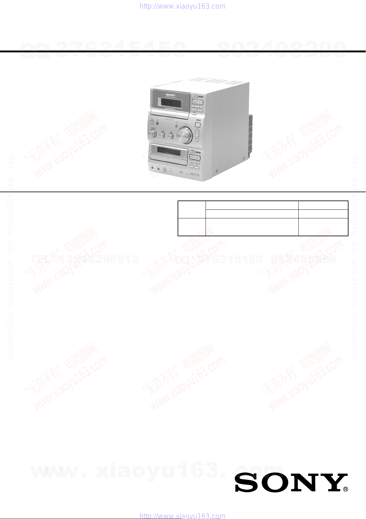
Sony HCD-VP100 User manual

SERVICE MANUAL
MICRO Hi-Fi COMPONENT SYSTEM
E Model
SPECIFICATIONS
HCD-VP100
Ver 1.0 2001.04
HCD-VP100 is the Amplifier, Video CD
player, Tape Deck and Tuner section in
CMT-VP100.
– Continued on next page –
Amplifier section
The following measured at 230 V AC, 60 Hz
DIN power output (rated): 27 + 27 W
(6 ohms at 1 kHz, DIN)
Continuous RMS power output (reference):
32 + 32 W
(6 ohms at 1 kHz, 10%
THD)
The following measured at 220 V AC, 60 Hz
DIN power output (rated): 23 + 23 W
(6 ohms at 1 kHz, DIN)
Continuous RMS power output (reference):
26 + 26 W
(6 ohms at 1 kHz, 10%
THD)
Inputs
AUDIO IN MD (VIDEO) (phono jacks):
Sensitivity 500/250 mV,
impedance 47 kilohms
MIC IN (minijack): Sensitivity 1 mV,
impedance 10 kilohms
Outputs
OPTICAL DIGITAL OUT (CD):
Optical
VIDEO OUT (phono jack):max. output level 1 Vp-p,
unbalanced, Sync
negative, load impedance
75 ohms
PHONES (stereo minijack):
Accepts headphones with
an impedance of 8 ohms
or more
VIDEO CD/CD playersection
System Compact disc and digital
audio and video system
Laser Semiconductor laser
(λ= 780 nm)
Emission
duration: continuous
Wavelength 780 - 790 nm
Video color system format NTSC, PAL
OPTICAL DIGITAL OUT (CD)
(Square optical connector jack, rear panel)
Wavelength 660 nm
Output Level –18 dBm
Tape player section
Recording system 4-track 2-channel stereo
Frequency response 50 - 13,000 Hz (±3 dB),
using a Sony TYPE I
cassette
Wow and flutter ±0.15% W. Peak (IEC)
0.1% W. RMS (NAB)
±0.2% W. Peak (DIN)
Model Name Using Similar Mechanism NEW
CD Mechanism Type CDM55F-K6BD42A
Model Name Using Similar Mechanism HCD-CP100
CD
Section
Tape deck
Section
9-873-828-11 Sony Corporation
2001D0500-1 Home Audio Company
C2001.4 ShinagawaTec Service Manual Production Group
w
w
w
.
x
i
a
o
y
u
1
6
3
.
c
o
m
Q
Q
3
7
6
3
1
5
1
5
0
9
9
2
8
9
4
2
9
8
T
E
L
1
3
9
4
2
2
9
6
5
1
3
9
9
2
8
9
4
2
9
8
0
5
1
5
1
3
6
7
3
Q
Q
TEL 13942296513 QQ 376315150 892498299
http://www.xiaoyu163.com

2
HCD-VP100
General
Power requirements 110 - 120 V or 220 -
240 V AC , 50/60 Hz
Adjustable with voltage
selector
Power consumption 75 W
Dimensions (w/h/d) Approx. 190 ×252 ×
345 mm incl. projecting
parts and controls
Mass Approx. 5.6 kg
Supplied accessories Remote commander (1)
AM loop antenna (1)
FM wire antenna (1)
Batteries (2)
Video connecting cord (1)
Design and specifications are subject to change
without notice.
AM tunersection
Tuning range
Middle Eastern and Philippine models:
531 - 1,602 kHz
(with the tuning interval
set at 9 kHz)
Other models: 530 - 1,710 kHz
(with the tuning interval
set at 10 kHz)
531 - 1,602 kHz
(with the tuning interval
set at 9 kHz)
Antenna AM loop antenna, external
antenna terminal
Intermediate frequency 450 kHz
Tuner section
FM stereo, FM/AM superheterodyne tuner
FM tunersection
Tuning range 87.5 - 108.0 MHz
(50-kHz step)
Antenna FM wire antenna
Antenna terminals 75 ohm unbalanced
Intermediate frequency 10.7 MHz
TABLE OF CONTENTS
1. GENERAL
Location of Controls ....................................................... 4
Setting the Time .............................................................. 5
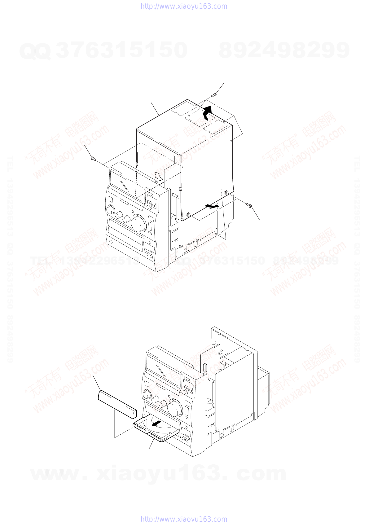
2. DISASSEMBLY
2-1. Disassembly Flow ........................................................... 7
2-2. Cover (Upper) ................................................................. 8
2-3. CD Lid ............................................................................. 8
2-4. Front Panel Section ......................................................... 9
2-5. Tape Mechanism Deck.................................................... 9
2-6. CD Mechanism Deck (CDM55F-K6BD42A),
MPEG Board ................................................................... 10
2-7. Base Unit (BU-K6BD42A)............................................. 10
2-8. Loading Board................................................................. 11
2-9. Cam (CDM55) ................................................................ 11
3. TEST MODE.............................................................. 12
4. ELECTRICAL ADJUSTMENTS
Deck Section ................................................................... 13
CD Section ...................................................................... 13
5. DIAGRAMS
5-1. Block Diagram –CD SERVO Section –........................ 14
5-2. Block Diagram –MAIN Section –................................. 15
5-3. Block Diagram
–DISPLAY/POWER SUPPLY Section –...................... 16
5-4. Note for Printed Wiring Boards and
Schematic Diagrams ....................................................... 17
5-5. Printed Wiring Board –CD Board –.............................. 18
5-6. Schematic Diagram –CD Board –................................. 19
5-7. Printed Wiring Board –TC Board –............................... 20
5-8. Schematic Diagram –TC Board –.................................. 21
5-9. Schematic Diagram
–MAIN (1/2)/LOADING Boards –............................... 22
5-10. Schematic Diagram –MAIN Board (2/2) –................... 23
5-11. Printed Wiring Boards
–MAIN/LOADING Boards –....................................... 24
5-12. Printed Wiring Boards
–SWITCH/TC SWITCH/PRISM Boards –................... 26
5-13. Schematic Diagram
–SWITCH/TC SWITCH/PRISM Boards –................... 27
5-14. IC Pin Function Description ........................................... 28
5-15. Printed Wiring Boards
–LCD/HEADPHONE/DIGITAL Boards –................... 29
5-16. Schematic Diagram
–LCD/HEADPHONE/DIGITAL Boards –................... 29
5-17. Printed Wiring Board –POWER Board –...................... 30
5-18. Schematic Diagram –POWER Board –......................... 31
6. EXPLODED VIEWS
6-1. Cover Section .................................................................. 34
6-2. Front Panel Section ......................................................... 35
6-3. Chassis Section ............................................................... 36
6-4. CD Mechanism Deck (CDM55F-K6BD42A)................ 37
6-5. Base Unit (BU-K6BD42A)............................................. 38
7. ELECTRICAL PARTS LIST ............................... 39
w
w
w
.
x
i
a
o
y
u
1
6
3
.
c
o
m
Q
Q
3
7
6
3
1
5
1
5
0
9
9
2
8
9
4
2
9
8
T
E
L
1
3
9
4
2
2
9
6
5
1
3
9
9
2
8
9
4
2
9
8
0
5
1
5
1
3
6
7
3
Q
Q
TEL 13942296513 QQ 376315150 892498299
http://www.xiaoyu163.com

3
HCD-VP100
CAUTION
Use of controls or adjustments or performance of procedures
other than those specified herein may result in hazardous ra-
diation exposure.
This appliance is classified as a CLASS 1 LASER product.
The CLASS 1 LASER PRODUCT MARKING is located on
the rear exterior.
Laser component in this product is capable of emitting radiation
exceeding the limit for Class 1.
The following caution label is located inside the unit.
CAUTION :
INVISIBLE LASER RADIATION WHEN OPEN AND
INTERLOCKS DEFEATED. AVOID EXPOSURE TO BEAM.
ADVARSEL :
USYNLIG LASERSTRÅLING VED ÅBNING NÅR
SIKKERHEDSAFBRYDERE ER UDE AF FUNKTION. UNDGÅ UDSAETTELSE
FOR STRÅLING.
VORSICHT :
UNSICHTBARE LASERSTRAHLUNG, WENN
ABDECKUNG GEÖFFNET UND SICHEREITSVERRIEGELUNG
ÜBERBRÜCKT. NICHT DEM STRAHL AUSSETZEN.
VARO!:
AVATTAESSA JA SUOJALUKITUS OHITETTAESSA OLET ALT-
TIINA NÄKYMÄTTÖMÄLLE LASERSÄTEILYLLE. ÄLÄ KATSO SÄTEESEEN.
VARNING :
OSYNLING LASERSTRÅLING NÄR DENNA DEL ÄR ÖPPNAD
OCH SPÄRREN ÄR URKOPPLAD.BETRAKTA EJ STRÅLEN.
ADVERSEL :
USYNLIG LASERSTRÅLING NÅR DEKSEL ÅPNES OG
SIKKERHEDSLÅS BRYTES. UNNGÅ EKSPONERING FOR STRÅLEN.
VIGYAZAT!:
A BURKOLAT NYITÁSAKOR LÁTHATATLAN LÉZERSU-
GÁRVESZÉLY!KERÜLJE A BESUGÁRZÁST!
Notes on chip component replacement
•Never reuse a disconnected chip component.
•Notice that the minus side of a tantalum capacitor may be dam-
aged by heat.
Flexible Circuit Board Repairing
•Keep the temperature of the soldering iron around 270 ˚C dur-
ing repairing.
•Do not touch the soldering iron on the same conductor of the
circuit board (within 3 times).
•Be careful not to apply force on the conductor when soldering
or unsoldering.
SAFETY-RELATED COMPONENT WARNING!!
COMPONENTS IDENTIFIED BY MARK 0OR DOTTED
LINE WITH MARK 0ON THE SCHEMATIC DIAGRAMS
AND IN THE PARTS LIST ARE CRITICAL TO SAFE
OPERATION. REPLACE THESE COMPONENTS WITH
SONY PARTS WHOSE PART NUMBERS APPEAR AS
SHOWN IN THIS MANUAL OR IN SUPPLEMENTS PUB-
LISHED BY SONY.
The laser diode in the optical pick-up block may suffer electro-
static break-down because of the potential difference generated
by the charged electrostatic load, etc. on clothing and the human
body.
During repair, pay attention to electrostatic break-down and also
use the procedure in the printed matter which is included in the
repair parts.
The flexible board is easily damaged and should be handled with
care.
NOTES ON LASER DIODE EMISSION CHECK
The laser beam on this model is concentrated so as to be focused
on the disc reflective surface by the objective lens in the optical
pick-up block. Therefore, when checking the laser diode emis-
sion, observe from more than 30 cm away from the objective lens.
SERVICE POSITION
In checking the CD block, prepare jig (extension cable J-2501-
011-B).
NOTES ON HANDLING THE OPTICAL PICK-UP
BLOCK OR BASE UNIT
Connect jig (extension cable J-2501-011-B)
to the MAIN board (CN101) and VCD block (CN502).
MAIN board
VCD block
w
w
w
.
x
i
a
o
y
u
1
6
3
.
c
o
m
Q
Q
3
7
6
3
1
5
1
5
0
9
9
2
8
9
4
2
9
8
T
E
L
1
3
9
4
2
2
9
6
5
1
3
9
9
2
8
9
4
2
9
8
0
5
1
5
1
3
6
7
3
Q
Q
TEL 13942296513 QQ 376315150 892498299
http://www.xiaoyu163.com

4
HCD-VP100 SECTION 1
GENERAL
• LOCATION OF CONTROLS
– FrontView –
)
A
Z
Y
?/1
x
mM
zX
Z
ux
.>
mM
1 2 5 8
9
q;
wj
qd
qf
qg
qj
qk
qa
63 4 7
ql
w;
wawdwfwgwh ws
qs
qh
BASS 3(20)
CD EJECT Zqj (9~11)
CD SYNC qs (17, 18)
CD uws (9~13, 28)
CD xqk (9~13, 26)
CD ./>ql (10~12)
CD m/Mql (10, 11)
DSG 5(20, 23)
FUNCTION wj (9, 11, 12, 14, 16,
17, 23)
MIC IN jack wg (20)
MIC VOL wf (20)
PBC indicator wd (10, 28)
PHONES jack wh
PLAY MODE wa (9, 11, 12, 18)
Remote sensor 2
REPEAT w; (10, 11)
TAPE EJECT Z8(16)
TAPE REC z6(17)
TAPE Y7(16~18)
TAPE Xqa (16~18)
TAPE x9(16~18, 26)
TAPE m/M0(16)
TREBLE 4(20)
TUNER BAND qd (14, 26)
TUNING MODE qg (14, 15)
TUNING +/– qf (14, 15)
VOLUME qh (21)
BUTTON DESCRIPTIONS
@/1 (power) 1(7, 14, 18, 21, 23
4
This section is extracted from
instruction manual.
w
w
w
.
x
i
a
o
y
u
1
6
3
.
c
o
m
Q
Q
3
7
6
3
1
5
1
5
0
9
9
2
8
9
4
2
9
8
T
E
L
1
3
9
4
2
2
9
6
5
1
3
9
9
2
8
9
4
2
9
8
0
5
1
5
1
3
6
7
3
Q
Q
TEL 13942296513 QQ 376315150 892498299
http://www.xiaoyu163.com

5
HCD-VP100
–Rear View –
5
6
7
8
1
2
3
4
1AM ANTENNA terminals
2AUDIO IN MD (VIDEO) jacks
3CD DIGITAL OUT OPTICAL connector
4SPEAKER terminals
5SYSTEM SELECT switch
6VIDEO OUT jack
7VOLTAGE SELECTOR switch
8AC power cord
8
Setting the time
1
Turn on the system.
2
Press CLOCK/TIMER SET on the
remote.
If you are setting the clock for the first time,
go to step 5.
3
Press +/–on the remote repeatedly
until “SET CLOCK”appears in the
display.
4
Press ENTER on the remote.
The hour indication flashes.
5
Press +/–on the remote repeatedly to
set the hour.
6
Press ENTER on the remote.
The minute indication flashes.
7
Press +/–on the remote repeatedly to
set the minute.
8
Press ENTER on the remote.
The clock will begin operating.
To resetthesystemclock
Start over from step 1.
w
w
w
.
x
i
a
o
y
u
1
6
3
.
c
o
m
Q
Q
3
7
6
3
1
5
1
5
0
9
9
2
8
9
4
2
9
8
T
E
L
1
3
9
4
2
2
9
6
5
1
3
9
9
2
8
9
4
2
9
8
0
5
1
5
1
3
6
7
3
Q
Q
TEL 13942296513 QQ 376315150 892498299
http://www.xiaoyu163.com

6
HCD-VP100
Remote Control
`/1
X
O
#
2
y
12
3
4
5
6
7
8
9
qj
qk
ql
w;
wa
wf
wg
wh
wj
wk
wl
wd
ws
q;
qa
qs
qd
qf
qg
qh
CD ql (9, 11)
CLOCK/TIMER SELECT 4
(19, 22)
CLOCK/TIMER SET 5(8, 18,
21)
DIR MODE wh (16~18)
DISPLAY wj (12)
ENTER 8(8, 14, 18, 21)
FUNCTION qj (9, 11, 12, 14, 16,
17, 23)
KEY CONTROL #/2qh (20)
K.PON/MPX 9(20)
MEMORY wk (14)
NEXT qa (10)
Numeric buttons wg (10, 11)
ON SCREEN 7(13)
PREV ws (10)
RETURN Oqs (10)
SLEEP wl (21)
SLOW ywd (9)
STEREO/MONO 6(15)
TAPE qk (16)
TUNER BAND qf (14)
TV/VIDEO 1(7)
TV @/12(7)
VOLUME +/–qg (21)
BUTTON DESCRIPTIONS
Nwa (9~13, 16~18, 28)
Xw; (9, 11, 16~18)
xqd (9~13, 16~18)
.ws (10~12)
>qa (10~12)
mwf (10, 11, 14~16)
Mq; (10, 11, 14~16)
@/1 (power) 3(7, 14, 18, 21)
+ qa (8, 14, 18, 21)
–ws (8, 14, 18, 21)
5
w
w
w
.
x
i
a
o
y
u
1
6
3
.
c
o
m
Q
Q
3
7
6
3
1
5
1
5
0
9
9
2
8
9
4
2
9
8
T
E
L
1
3
9
4
2
2
9
6
5
1
3
9
9
2
8
9
4
2
9
8
0
5
1
5
1
3
6
7
3
Q
Q
TEL 13942296513 QQ 376315150 892498299
http://www.xiaoyu163.com

HCD-VP100
7
• This set can be disassembled in the order shown below.
2-1. DISASSEMBLY FLOW
SECTION 2
DISASSEMBLY
2-2. COVER (UPPER)
(Page 8)
Set
2-4. FRONT PANEL SECTION
(Page 9)
2-3. CD LID
(Page 8)
2-5.TAPE MECHANISM DECK
(Page 9)
2-7. BASE UNIT
(BU-K6BD42A)
(Page 10)
2-8. LOADING BOARD
(Page 11)
2-9. CAM (CDM55)
(Page 11)
2-6. CD MECHANISM DECK
(CDM55F-K6BD42A),
MPEG BOARD
(Page 10)
w
w
w
.
x
i
a
o
y
u
1
6
3
.
c
o
m
Q
Q
3
7
6
3
1
5
1
5
0
9
9
2
8
9
4
2
9
8
T
E
L
1
3
9
4
2
2
9
6
5
1
3
9
9
2
8
9
4
2
9
8
0
5
1
5
1
3
6
7
3
Q
Q
TEL 13942296513 QQ 376315150 892498299
http://www.xiaoyu163.com

HCD-VP100
8
2-3. CD LID
Note: Follow the disassembly procedure in the numerical order given.
2-2. COVER (UPPER)
1
four screws
(BVTP4
×
8)
2
two case screw
s
2
two case screws
3
cover (upper)
2
CD lid
1
tray
Note: Open the tray by supplying the power.
w
w
w
.
x
i
a
o
y
u
1
6
3
.
c
o
m
Q
Q
3
7
6
3
1
5
1
5
0
9
9
2
8
9
4
2
9
8
T
E
L
1
3
9
4
2
2
9
6
5
1
3
9
9
2
8
9
4
2
9
8
0
5
1
5
1
3
6
7
3
Q
Q
TEL 13942296513 QQ 376315150 892498299
http://www.xiaoyu163.com

HCD-VP100
9
2-4. FRONT PANEL SECTION
2-5. TAPE MECHANISM DECK
1
wire (flat type) 18p
(CN802)
1
wire (flat type) 20p
(CN804)
1
wire (flat type) 23p
(CN801)
2
connector
(CN501)
3
two screws
(BTP3
×
8)
4
screw (KTP3
×
6)
4
screw (KTP3
×
6)
1
wire (flat type) 21p
(CN301)
5
front panel section
1
three screws
(BVTT2.6
×
5
)
6
two screws
(BTP3
×
8)
6
two screws
(BTP3
×
8)
7
tape machanism deck
4
TC board
5
wire (flat type) 9P
(CN302)
3
connector
(CNP1)
2
w
w
w
.
x
i
a
o
y
u
1
6
3
.
c
o
m
Q
Q
3
7
6
3
1
5
1
5
0
9
9
2
8
9
4
2
9
8
T
E
L
1
3
9
4
2
2
9
6
5
1
3
9
9
2
8
9
4
2
9
8
0
5
1
5
1
3
6
7
3
Q
Q
TEL 13942296513 QQ 376315150 892498299
http://www.xiaoyu163.com

HCD-VP100
10
2-6. CD MECHANISM DECK (CDM55F-K6BD42A), MPEG BOARD
2-7. BASE UNIT (BU-K6BD42A)
4
two screws
(BTP3
×
8)
7
three screws
(DIA.2.6
×
8)
3
connector
(CN503)
3
connector
(CN504)
9
two screws
(DIA.2.6
×
8)
0
bracket (MPEG)
8
MPEG board
qa
CD mechanism deck
(CDM55F-K6BD42A)
5
2
connector
(CN401)
1
flexible flat cable
(19core) (CN101)
6
flexible flat cable
(24core) (CN501)
1
floating screw
(PTPWHM2.6)
2
base unit
(BU-K6BD42A)
w
w
w
.
x
i
a
o
y
u
1
6
3
.
c
o
m
Q
Q
3
7
6
3
1
5
1
5
0
9
9
2
8
9
4
2
9
8
T
E
L
1
3
9
4
2
2
9
6
5
1
3
9
9
2
8
9
4
2
9
8
0
5
1
5
1
3
6
7
3
Q
Q
TEL 13942296513 QQ 376315150 892498299
http://www.xiaoyu163.com

HCD-VP100
11
2-8. LOADING BOARD
2-9. CAM (CDM55)
2
belt (CDM55)
B
3
Pull the tray
with pushing
B
.
4
two screws
(BTP2.6
×
6)
5
LOADING board
1
Rotate the gear(B) in
the direction of arrow
A
.
A
2lever (SW)
1torsion spring
6gear (B)
3spacer (55)
4pulley (LDG)
5gear (A)
7roller
8cam (CDM55)
w
w
w
.
x
i
a
o
y
u
1
6
3
.
c
o
m
Q
Q
3
7
6
3
1
5
1
5
0
9
9
2
8
9
4
2
9
8
T
E
L
1
3
9
4
2
2
9
6
5
1
3
9
9
2
8
9
4
2
9
8
0
5
1
5
1
3
6
7
3
Q
Q
TEL 13942296513 QQ 376315150 892498299
http://www.xiaoyu163.com

HCD-VP100
12
SECTION 3
TEST MODE
Start
REC pause for 3 seconds
FWD REC
Fast forward
REV Play
REC pause for 3 seconds
REV REC
Rewind
FWD Play Shut off
Shut off
Shut off
Shut off
1 minute
3 minutes
1 minute
3 minutes
Start
Open the disc tray
Close the disc tray
Play the last track
[Cold Reset]
• The cold reset clears all data including preset data stored in the
RAM to initial conditions. Execute this mode when returning
the set to the customer.
Procedure:
1. Turn ON the power.
2. Press three buttons x(TAPE), x(CD), and [BAND]
simultaneously.
3. The set is reset.
[Liquid Crystal Display All Lit Check Mode]
Procedure:
1. Set to standby state.
2. Press three buttons of x(TAPE), x(CD), and
[TUNING MODE] simultaneously.
3. Liquid crystal display are all turned on.
4. To exit from this mode, press the I/1button to turn the power
OFF.
[Tape Deck Aging Mode]
This mode can be used for operation check of tape deck section.
Procedure:
1. Set a tape in the tape deck.
2. Set to standby state.
3. Press three buttons of x(TAPE), x(CD), and [TUNING +]
simultaneously.
4. The aging is executed in bellow sequence.
5. To exit from the aging mode, press the I/1button to turn the
power OFF.
Aging mode sequence:
[CD Aging Mode]
This mode can be used for operation check of CD section.
Procedure:
1. Load a CD disc.
2. Set to standby state.
3. Press three buttons of x(TAPE), x(CD), and [TUNING --]
simultaneously.
4. The aging is executed in bellow sequence.
5. To exit from the aging mode, press the I/1button to turn the
power OFF.
Aging mode sequence:
w
w
w
.
x
i
a
o
y
u
1
6
3
.
c
o
m
Q
Q
3
7
6
3
1
5
1
5
0
9
9
2
8
9
4
2
9
8
T
E
L
1
3
9
4
2
2
9
6
5
1
3
9
9
2
8
9
4
2
9
8
0
5
1
5
1
3
6
7
3
Q
Q
TEL 13942296513 QQ 376315150 892498299
http://www.xiaoyu163.com

HCD-VP100
1313
2. Turn the adjustment screw and check output peaks. If the peaks
do not match for L-CH and R-CH, turn the adjustment screw
so that outputs match within 1dB of peak.
3. Mode: Playback
4. Repeat step 1 to 3 in playback (REV) mode.
5. After the adjustments, apply suitable locking compound to the
pats adjusted.
Adjustment Location:
SECTION 4
ELECTRICAL ADJUSTMENTS
0 dB=0.775 V
DECK SECTION
Tape Signal Used for
P-4-A100 10 kHz, –10 dB Azimuth Adjustment
WS-48B 3 kHz, 0 dB Tape Speed Adjustment
P-4-L300 315 Hz, 0 dB Level Adjustment
Note: Confirm each contents of this section first of all. If the results are
not satisfied, do the adjustment.
1. Demagnetize the record/playback head with a head
demagnetizer.
2. Do not use a magnetized screwdriver for the adjustments.
3. After the adjustments, apply suitable locking compound to the
parts adjust.
4. The adjustments should be performed with the rated power
supply voltage unless otherwise noted.
5. The adjustments should be performed in the order given in this
service manual. (As a general rule, playback circuit adjustment
should be completed before performing recording circuit
adjustment.)
6. The adjustments should be performed for both L-CH and R-
CH.
7. Switches and controls should be set as follows unless otherwise
specified.
• Test Tape
Record/Playback Head Azimuth Adjustment
Procedure:
1. Mode: Playback
set
MAIN board
SPEAKER terminals (SJ301
)
L-CH, R-CH
+
–
level meter
test tape
P-4-A100
(10 kHz, –10 dB)
Screw
position
L-CH
peak
within
1 dB
Output
level
L-CH
peak
R-CH
peak
within
1 dB
Screw
position
R-CH
peak
MAIN
board
CN301
set
test tape
P-4-A100
(10 kHz, –10 dB)
R-CH
oscilloscope
L-CH
R-CH
VH
waveform of oscilloscope
in phase 45°90°135 °180°
good wrong
MAIN board
SPEAKER terminals (SJ301)
L-CH
forward
reverse
CD SECTION
Notes:
1. CD block basically constructed to operate without adjustment. There-
fore, check each item in order given.
2. UseYEDS-18 disc (Part No.: 3-702-101-01) unless otherwise indicated.
3. Use the oscilloscope with more than 10 MΩimpedance.
4. Clean an object lens by an applicator with neutral detergent when the
signal level is low than specified value with the following checks.
S-Curve Confirmation
Connection:
Procedure:
1. Connect an oscilloscope to IC703 pin qg and TP (VC) on the
CD board.
2. Connect between TP (FOK) and TP (GND) on the CD board
by lead wire.
3. Turn the power ON.
4. Press the [EJECT ] (CD) button to open the disc tray, and
put the disc (YEDS-18).
5. Press the [EJECT ] (CD) button to close the disc tray (Actu-
ate the focus search).
6. Confirm that the waveform on the oscilloscope is symmetrical
between A and B and that peak to peak level is within 3.0 ±
1.0 Vp-p.
S-curve waveform
7. After confirmation, disconnect the lead wire in step 2.
Note: • Try to measure several times to make sure that the ratio of A : B
or B : A is more than 10 : 7.
• Take sweep time as long as possible and light up the brightness
to obtain best waveform.
RF Level Confirmation
Connection:
Procedure:
1. Connect an oscilloscope to IC703 pin qh and TP (VC) on the
CD board.
2. Turn the power ON.
3. Load the disc (YEDS-18), and press the [ ] button to play-
back the disc.
4. Confirm that the waveform on the oscilloscope is clear and
that the RF signal level is correct.
Note: Clear RF signal waveform means that the shape “◊” can be clearly
distinguished at the center of the waveform.
+
–
CD board
IC703 pin qg
TP (VC)
oscilloscope
+
–
CD board
IC703 pin qh
TP (VC)
oscilloscope
(AC range)
RF signal waveform
When observing the eye pattern, set the oscilloscope for AC range
and raise vertical sensitivity.
Connecting Location:
– CD Board (Conductor Side) –
VOLT/DIV: 200 mV
TIME/DIV: 500 ns
(with the 10: 1 probe
in use)
level: 1.3 Vp-p
+0.25
–0.20
Z
within 3.0
±
1.0 Vp-p
A
B
symmetry
TP (GND)
TP (VC)
TP (FOK) 20 11
110
CN701
IC701
IC703
u
Z
w
w
w
.
x
i
a
o
y
u
1
6
3
.
c
o
m
Q
Q
3
7
6
3
1
5
1
5
0
9
9
2
8
9
4
2
9
8
T
E
L
1
3
9
4
2
2
9
6
5
1
3
9
9
2
8
9
4
2
9
8
0
5
1
5
1
3
6
7
3
Q
Q
TEL 13942296513 QQ 376315150 892498299
http://www.xiaoyu163.com

HCD-VP100
1414
VCD BLOCK
A/D
CONVERTER
OUT+
OUT–
3
4
7
2
1
5
10
6
4
5
6
16
15
14
13
8
9
19
2
1
77
78
71
55
54
45
47
46
6320
31 33 34 32
36
38
39
26
93
27
28 29
80
88
89
100
2
4
6
8
10
20
19
10
9
4
5
16
17
27
26
23, 24
E
B
C
D
A
A+5V
F
DETECTOR
A
B
C
D
RF
SUMMING
AMP
FOCUS
ERROR AMP
RF EQ
SWITCH
Q702
RF EQ
AMP
TRACKING
ERROR AMP
RFO
17
RFE
FE
FE BIAS
RF AMP,
FOCUS/TRACKING ERROR AMP
IC703
TE
E
FF I-V AMP
E I-V AMP
AUTOMATIC
POWER
CONTROL
Q701
OPTICAL
TRANSCEIVER
IC321
OPTICAL
DIGITAL OUT (CD)
APC LD
AMP
APC PD
AMP
LD
LD
PD
LASER DIODE
RFAC MIX
ASYO
ASYI
FILTER
FILO
PCO
CLTV
FILI
DIGITAL PLL
ASYMMETRY
CORRECTOR
EFM
DEMODULATOR REGISTER
DIGITAL SIGNAL PROCESSOR
IC701 (1/2)
MON
MDP
MDS
94 95 96 97
FSW
CLV
PROCESSOR
18-TIMES
OVERSAMPLING
FILTER
NOISE
SHAPER
INTERNAL BUS
32K
RAM
ERROR
CORRECTOR
SUBQ
SQCK
83
SCLK
79
MUTE
76
EXCK
SUBCODE Q
PROCESSOR
SUBCODE P – W
PROCESSOR
SYNC
PROTECTOR
TIMING
GENERATOR 1
TIMING
GENERATOR 2
DATA
VCKI
XTAO
62
XTAI
BCLK
LRCK
RFCK
GFS
56
C2PO
DOUT
DIGITAL
OUT
SERIAL/PARALLEL
PROCESSOR
D/A DIGITAL
PROCESSOR
CLOCK
GENERATOR
ADDRESS
GENERATOR
PRIORITY
ENCODER
PEAK
DETECTOR
74
SCOR
81 73
WFCK
75
SBSO
SE
TE
FE
RFDC
FOCUS/TRACKING/SLED
SERVO DSP
FOCUS/TRACKING/SLED
PWM GENERATOR
SFDR
IN+
IN–
OUT+
OUT–
IN–
IN+
IN–
IN+
15
MUTE
SRDR
TFDR
TRDR
FFDR
FRDR
COUT
MIRR/DFCT/
FOK
DETECTOR
SERVO AUTO
SEQUENCER
SERVO
INTERFACE
CPU
INTERFACE
CLOK 86
DATA
87
XLAT
SENS
FOK
91
92
MIRR
DFCT
IN+, IN–
OUT+
OUT–
M101
(SPINDLE)
MOTOR
DRIVE
LDON
MUTE
MOTOR
DRIVE
COIL
DRIVE
OUT–
OUT+
COIL
DRIVE
M
M
M102
(SLED)
FOCUS/TRACKING COIL DRIVE,
SPINDLE/SLED MOTOR DRIVE
IC702
2-AXIS
DEVICE
(TRACKING)
(FOCUS)
DIGITAL SERVO
PROCESSOR
IC701 (2/2)
OPTICAL PICK-UP
(KSS-213DCP)
LDON
PD
I-V AMP
12
13
2
1
SUBQ
SQCK/SCLK
SCOR
VARI-PITCH
DOUBLE SPEED
IC704
D+5V
S901
DISC TRAY
OPEN/CLOSE DETECT
INPUT1TR-CLOSE OUT1
LOADING
MOTOR DRIVE
IC320
SW-CLOSE
SW-OPEN
5 2
INPUT2
TR-OPEN OUT2
6 10 M
M901
(LOADING)
FOK
SENS
DATA
CLK
XTL
XRST
XRST
PAL
AUTO
NTSC
SW401
SYSTEM SELECT
CTRL2
XTAL 16.9344MHz
AD
BCK
LRCK
C2PO
DO DO
VIDEO OUT J401
VIDEO OUT
A +5V
S101
(LIMIT)
LIMIT
GFS
VIDEO SYSTEM
A(Page 15)
CD L-CH
L-OUT
R-OUT R-CH
S-REQ
S-CLK
S-ACK
RST
S-SD
S-SI
E(Page 15)
• SIGNAL PATH
: CD PLAY (ANALOG OUT)
• R-CH : R-ch is omitted due to same as L-ch.
: CD PLAY (DIGITAL OUT)
: CD PLAY (VIDEO)
SECTION 5
DIAGRAMS
5-1. BLOCK DIAGRAM – CD SERVO Section –
w
w
w
.
x
i
a
o
y
u
1
6
3
.
c
o
m
Q
Q
3
7
6
3
1
5
1
5
0
9
9
2
8
9
4
2
9
8
T
E
L
1
3
9
4
2
2
9
6
5
1
3
9
9
2
8
9
4
2
9
8
0
5
1
5
1
3
6
7
3
Q
Q
TEL 13942296513 QQ 376315150 892498299
http://www.xiaoyu163.com

HCD-VP100
1515
5-2. BLOCK DIAGRAM – MAIN Section –
TU1
TUNER PACK
L
R
1
2
4
9
8
10
7
31 30 17 3
LINE
OUT2 VOL2 OUT2
TREBLE
LOGIC
MIDDLE BASS
INPUT SELECT SWITCH,
MIX, TONE CONTROL,
ELECTRICAL VOLUME
IC323
12
13
2
14 15
88 23
5
8
19
18
25
AUDIO IN
MD (VIDEO)
SJ302
HRPE901
(RECORD/PLAYBACK/ERASE)
R-CH
(ERASE)
R-CH
L-CH
1
3
2
REC/PB SWITCHING
IC402
REC/PB AMP, EQ AMP
IC401
(REC)
(PB) (SW)
R-CH
R-CH
4
23
24 20
R-CH
R-CH ALC
16
14
REC OUT L
PB L
REC
IN L
B+
(+8V)
BIAS
OSC
T401
REC BIAS SWITCH
Q402, 403
BIAS OSC
Q401
BIAS
TRAP
T403
CD L-CH
S-ACK
S-REQ
S-DO
S-DI
S-CLK
S-RST
DATA CLK
SDA
(JOG G)
SCK
95
11 86 14 100
E
(Page 14)
MUTING
Q200
R-CH
B+ (+8V)
MUTING DRIVE
Q330
4
10 9
14
+
+
–
–
SJ301
L
R
SPEAKER
IMPEADANCE
USE 6 –16Ω
R-CH
R-CH J301
HEADPHONE AMP
IC324
MUTING
Q815, 817
MUTING DRIVE
Q312, 313
MOS GAIN &
LEVEL SHIFT
ING STAGE
MOS
OUTPUT
STAGE
SHORT
CIRCUIT
PROTECTION
TUNER
D856, 857
IN+
IN–
STANDBY/MUTE
MUTE STBY
B(Page 16)
REG CON
D(PAGE 16)
REC/PB
POWER AMP
IC201
R-CH
97
22
24
93
92
X802
32.768KHz
39
4
40
X801
4.19MHz
CAPSTAN/REEL
MOTOR DRIVE
Q601, 602
10
1
6
32
TRIGGER
PLUNGER DRIVE
Q603, 604
MM
TAPE END DETECT
SENSOR
(TAPE DECK BLOCK)
•SIGNAL PATH
: TUNER
: CD PLAY (ANALOG OUT)
: CD PLAY (OPTICAL OUT)
: TAPE (PLAY)
: TAPE (RECORD)
: MD
OUT
FM ANT
ANT GND
ANT GND
AM ANT
L-CH
R-CH R-CH
TUNED
DI
CK
CE
DO
R-CH
B IN L
A IN L
6
2
8
10
SYSTEM CONTROLLER
IC801 (1/2)
C2
A2
D2
E2
(S-SI)
(S SO)
TUNED
(TU-DATA)
(TU-CLK)
(TU-CE)
(TU-COUNT)
TU ON
REC/PB
(S-CLK)
(MPEG-RST)
(S-REQ)
(S-ACK)
AU-MUTE
AMP-MUTE
(MIC CHECK)
TEX
TX
EXTAL1
MOT-CON
XTAL1
SOL-CON
TAPE-END
T-MODE
TC SW
PHONES
•R-CH : R-ch is omitted due to same as L-ch.
A
(Page 14)
96
87
L-MUTE
REC-MUTE
MUTING
Q407
MUTING
Q414
R-CH
R-CH
LINE
AMP
MIC AMP
11
R-CH
D401
R-CH R-CH
J402
MIC IN
RV200
MIC VOL
2157
MIC AMP
IC325
LED DRIVE
Q854
FM
75Ω
AM
ANTENNA
MIC CONTROL
Q394 –397
: MIC
w
w
w
.
x
i
a
o
y
u
1
6
3
.
c
o
m
Q
Q
3
7
6
3
1
5
1
5
0
9
9
2
8
9
4
2
9
8
T
E
L
1
3
9
4
2
2
9
6
5
1
3
9
9
2
8
9
4
2
9
8
0
5
1
5
1
3
6
7
3
Q
Q
TEL 13942296513 QQ 376315150 892498299
http://www.xiaoyu163.com

HCD-VP100
1616
5-3. BLOCK DIAGRAM – DISPLAY/POWER SUPPLY Section –
ROTARY
ENCODER
RV801
VOLUME
RV801
FUNCTION
RV804
ROTARY
ENCODER
RV802
TREBLE
RV802
ROTARY
ENCODER
RV803
BASS
RV803
ROTARY
ENCODER
RV804
JOG-A
JOG-B
JOG E (TREBLE)
JOG F (TREBLE)
JOG C (BASS)
JOG D (BASS)
JOG-G
JOG-H
21
20
29
30
9
16
28
33
36 –34
KEY1 –3
S801 –820
50 –53
COM0 –3
LIQUID CRYSTAL
DISPLAY
LCD801
54 –85
SEG0 –31
REMOCON3
REMOTE CONTROL
RECEIVER
IC802
LED DRIVE
Q855
DSG
D858
CD SYNC
D859 LED DRIVE
Q856 CD-SYNC
26
27
89
38
99
VDD
RESET
WP
RESET SIGNAL
GENERATOR
IC803
+5V
(ROTARY ENCODER)
D812
D811
B+ SWITCH
Q606, 607
Q605
B+ SWITCH
Q608, 609
CASSETTE HOLDER
BACK LIGHT
D802
DREC/PB
(Page 15)
SYSTEM CONTROLLER
IC801 (2/2)
LED DRIVE
Q851
Q857
D851
D870, 871
(DISC TRAY ILLUMINATION)
LED DRIVE
Q853 TAPE
D854, 855
TC-ON 98
94CD-ON
LED DRIVE
Q852 CD
D852, 853
CD +5V
REGULATOR
Q306
B+
(CD +5V)
+10V
REGULATOR
Q305
CD +8V
REGULATOR
IC306
B+
(CD +8V)
B+
(FM +7.5V)
+9V
REGULATOR
Q301
FM +7.5V
REGULATOR
Q302
B+
(+9.5V)
B+
(COM +12V)
7
REG-CON
RECT
D906 –909
RECT
D902 –905
COM +8V
REGULATOR
IC304
COM +12V
REGULATOR
Q355
B+
(COM +8V)
LED B+
SWITCH
Q661, 662
LED B+
(+8V)
T902
MAIN
TRANSFORMER
RELAY
DRIVE
Q902
B+
(+14V)
B –
( –14V)
B+
(+22.5V)
B –
( –22.5V)
POWER AMP
(IC101, 201)
COM –8V
REGULATOR
IC302
B –
( COM –8V)
(Page 15) REG CON
CB
RY901
AC IN
D917
D310
B+ SWITCH
Q608, 609
B+ SWITCH
Q901
RECT
D910 –913
RELAY +5V
REGULATOR
IC301
T901
SUB
TRANSFORMER
WAKE UP
SWITCH
Q890, 891
D801
D S G
D866 –869
(LCD BACK LIGHT)
37SIMUKE/TEST
B+ (+5V)
REGULATOR
CONTROL
SWITCH
Q303, 304
REGULATOR
CONTROL
SWITCH
Q307, 308
STANDBY
B+
(+5V, RELAY +5V)
230V
115V
COM
COM
115V
230V
F902
-2
-1
VOLTAGE
SELECTOR
S901 220 –240V
110 –120V
15
(PCB-LED)
LED DRIVE
Q856
LED DRIVE
Q859
PBC
D860
31
(FM-ON)
F905
w
w
w
.
x
i
a
o
y
u
1
6
3
.
c
o
m
Q
Q
3
7
6
3
1
5
1
5
0
9
9
2
8
9
4
2
9
8
T
E
L
1
3
9
4
2
2
9
6
5
1
3
9
9
2
8
9
4
2
9
8
0
5
1
5
1
3
6
7
3
Q
Q
TEL 13942296513 QQ 376315150 892498299
http://www.xiaoyu163.com

HCD-VP100
1717
5-4. NOTE FOR PRINTED WIRING BOARDS AND SCHEMATIC DIAGRAMS
Note on Printed Wiring Boards:
•X: parts extracted from the component side.
•Y: parts extracted from the conductor side.
•W: indicates side identified with part number.
•: Pattern from the side which enables seeing.
• Indication of transistor.
Note on Schematic Diagram:
• All capacitors are in µF unless otherwise noted. pF: µµF
50 WV or less are not indicated except for electrolytics
and tantalums.
• All resistors are in Ωand 1/4W or less unless otherwise
specified.
•f: internal component.
•C: panel designation.
•A: B+ Line.
•B: B– Line.
•H: adjustment for repair.
• Voltages aretakenwith aVOM(Input impedance10 MΩ).
Voltage variations may be noted due to normal produc-
tion tolerances.
• Waveforms are taken with a oscilloscope.
Voltage variations may be noted due to normal produc-
tion tolerances.
• Circled numbers refer to waveforms.
• Signal path.
F:TUNER
E:TAPE PLAY (DECK A)
d:TAPE PLAY (DECK B)
G:TAPE REC
J: CD PLAY (ANALOG OUT)
c: CD PLAY (DIGITAL OUT)
N: MIC
• Abbreviation
EA : Saudi Arabia model
SP : Singapore model
TH :Thailand model
Note: The components identified by mark 0or dotted line
with mark 0are critical for safety.
Replace only with part number specified.
C
BThese are omitted.
E
Q
B
These are omitted.
CE
Q
B
These are omitted.
CE
Q
• Circuit Boards Location
TC board
PRISM board
LCD board
TC SWITCH board
SWITCH board
HEADPHONE board
MAIN board
TUNER UNI
T
POWER board DIGITAL boar
d
CD board
LOADING board
MPEG board
w
w
w
.
x
i
a
o
y
u
1
6
3
.
c
o
m
Q
Q
3
7
6
3
1
5
1
5
0
9
9
2
8
9
4
2
9
8
T
E
L
1
3
9
4
2
2
9
6
5
1
3
9
9
2
8
9
4
2
9
8
0
5
1
5
1
3
6
7
3
Q
Q
TEL 13942296513 QQ 376315150 892498299
http://www.xiaoyu163.com

HCD-VP100
1818
5-5. PRINTED WIRING BOARD – CD Board – • See page 17 for Circuit Boards Location.
CD BOARD
15
4
2
3
(CHASSIS)
24
TP
(VC)
TP
(RF) TP (TE)
TP (FE)
1
2
S101
(LIMIT)
1-680-690-
11
(11)
M
M101
(SPINDLE)
M
M102
(SLED)
OPTICAL PICK-UP
BLOCK
KSS-213 DCP
A
VCD BLOCK (1/2)
A
B
C
D
1 2 3 4 5
TP
(GND)
TP
(FOK)
IC701 B-2
IC702 C-3
IC703 B-3
IC704 C-1
Q701 B-3
Q702 A-2
• Semiconductor
Location
Ref. No. Location
(Page 24)
w
w
w
.
x
i
a
o
y
u
1
6
3
.
c
o
m
Q
Q
3
7
6
3
1
5
1
5
0
9
9
2
8
9
4
2
9
8
T
E
L
1
3
9
4
2
2
9
6
5
1
3
9
9
2
8
9
4
2
9
8
0
5
1
5
1
3
6
7
3
Q
Q
TEL 13942296513 QQ 376315150 892498299
http://www.xiaoyu163.com

HCD-VP100
1919
5-6. SCHEMATIC DIAGRAM – CD Board – • See page 25 forWaveforms. •See page 32 for IC Block Diagrams.
•Voltages and waveforms are dc with respect to ground
under no-signal conditions.
no mark : CD PLAY
∗: Impossible to measure
The components identified by mark 0or dotted
line with mark 0are critical for safety.
Replaceonly withpartnumber specified.
(Page
22)
w
w
w
.
x
i
a
o
y
u
1
6
3
.
c
o
m
Q
Q
3
7
6
3
1
5
1
5
0
9
9
2
8
9
4
2
9
8
T
E
L
1
3
9
4
2
2
9
6
5
1
3
9
9
2
8
9
4
2
9
8
0
5
1
5
1
3
6
7
3
Q
Q
TEL 13942296513 QQ 376315150 892498299
http://www.xiaoyu163.com

HCD-VP100
2020
5-7. PRINTED WIRING BOARD –TC Board – • See page 17 for Circuit Boards Location.
TAPE DECK BLOCK
SUPPLIED WITH
THE ASSEMBLED
BLOCK
B
MAIN BOARD
CN301 CASSETTE HOLDER
BACK LIGHT
2
HEAD
RELAY
BOARD
HRPE901
RECORD/PLAYBACK/ERASE
L-CH
R-CH
ERASE
1-681-239-
12
(12)
TC BOARD
8
17
A
B
C
D
E
1 2 3 4
E
D401
K
A
C420
D401 D-2
IC401 D-4
IC402 D-4
Q401 D-2
Q402 D-2
Q403 D-2
Q406 C-4
Q407 C-4
Q413 D-3
Q414 C-4
• Semiconductor
Location
Ref. No. Location
(Page 24)
w
w
w
.
x
i
a
o
y
u
1
6
3
.
c
o
m
Q
Q
3
7
6
3
1
5
1
5
0
9
9
2
8
9
4
2
9
8
T
E
L
1
3
9
4
2
2
9
6
5
1
3
9
9
2
8
9
4
2
9
8
0
5
1
5
1
3
6
7
3
Q
Q
TEL 13942296513 QQ 376315150 892498299
http://www.xiaoyu163.com
Table of contents
Other Sony Stereo System manuals

Sony
Sony CMT-CPX22 - Micro Hi Fi Component System User manual

Sony
Sony CMT-HP7 - Executive Microsystem User manual

Sony
Sony HCD-H11 User manual

Sony
Sony HCD-CP1 User manual

Sony
Sony SRS-BTX300 User guide

Sony
Sony MHC-G99AV User manual

Sony
Sony SRS-X5 User manual

Sony
Sony DHC-AZ1D User manual

Sony
Sony FH-B150 User manual

Sony
Sony HCD-GNX88 User manual

Sony
Sony SA-V90DW Reference guide

Sony
Sony CMT-EX5 - Micro Hi Fi Component System User manual

Sony
Sony WX-GT90BT User manual

Sony
Sony HCD-EP303 User manual

Sony
Sony MHC-C33 User manual

Sony
Sony GX255 User manual

Sony
Sony CMT-GB3 User manual

Sony
Sony CMT-LX20I Marketing User manual

Sony
Sony HCD-H1700 User manual

Sony
Sony MEX-N6000BD User manual