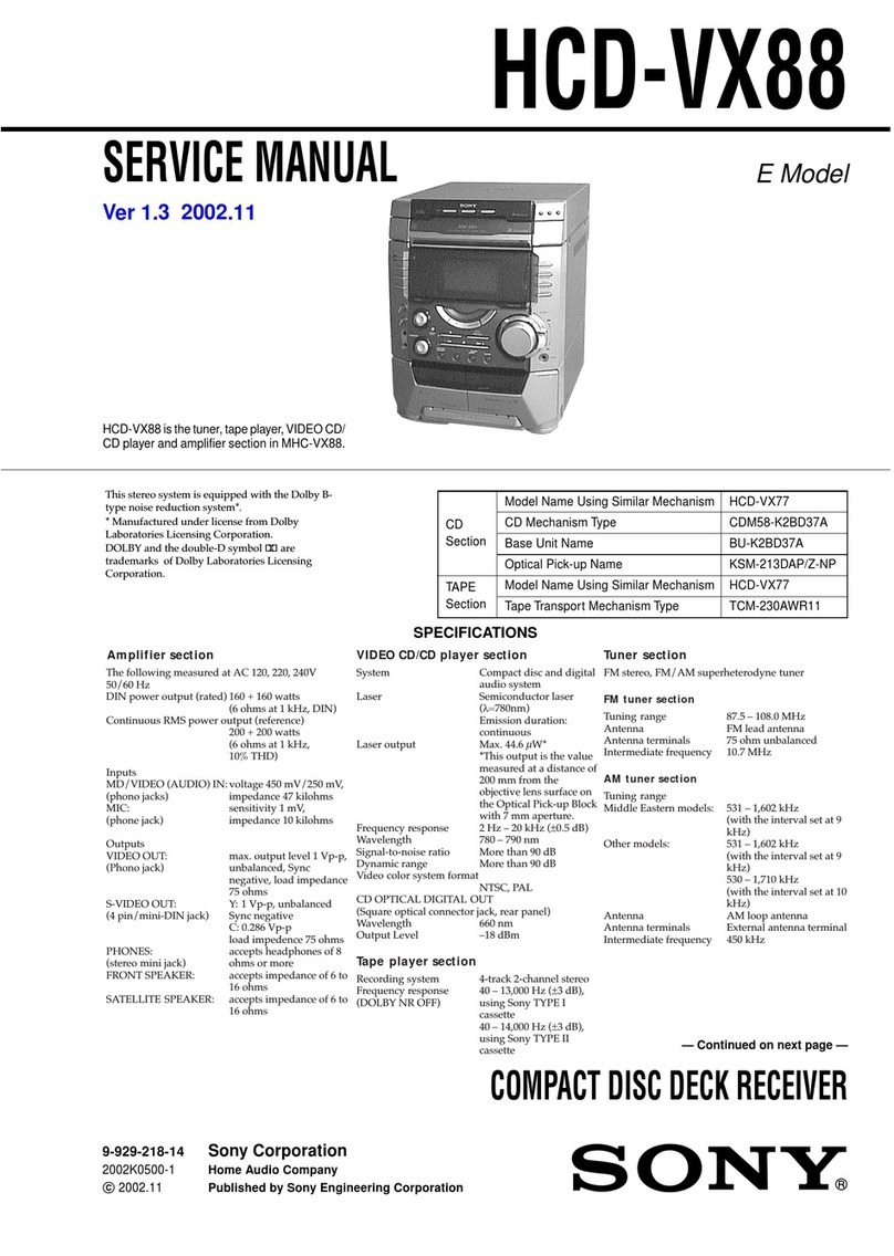
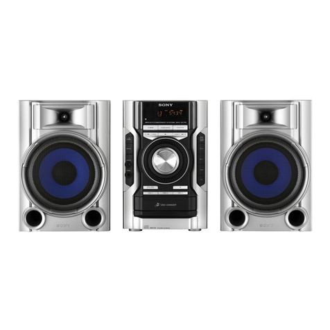
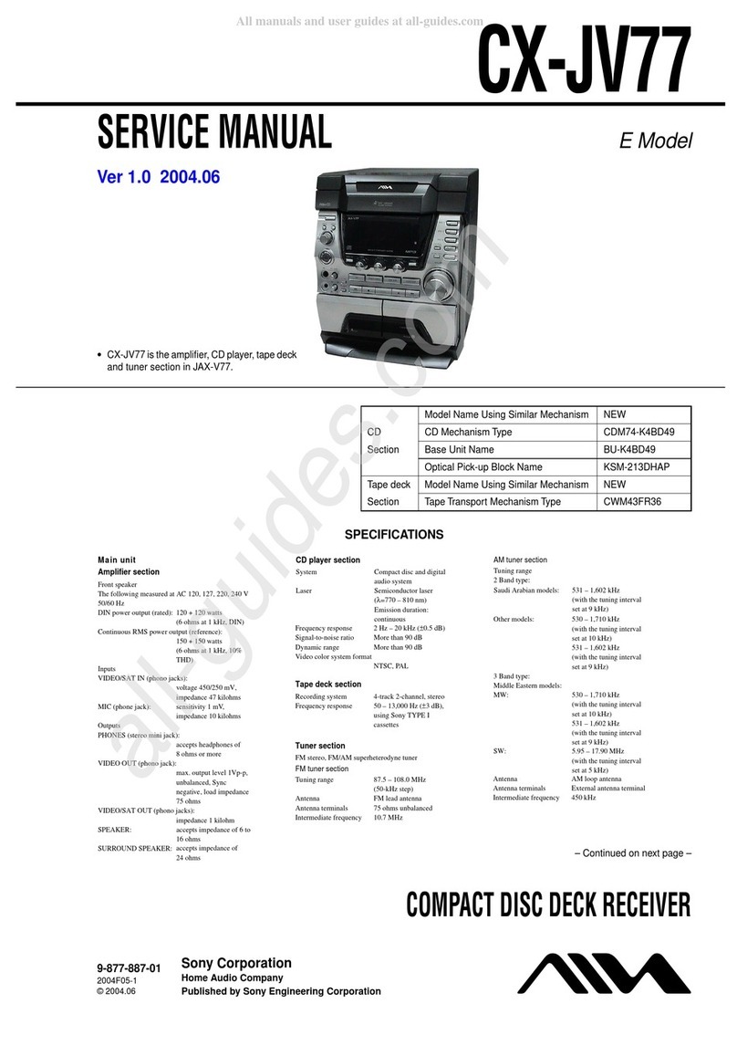
Sony CX-LFA500 User manual

CX-LFA500
AEP Model
UK Model
E Model
Australian Model
SERVICE MANUAL
MICRO HI-FI COMPONENT SYSTEM
Sony Corporation
Personal Audio Division
Published by Sony Engineering Corporation
9-877-166-05
2005J16-1
© 2005.10
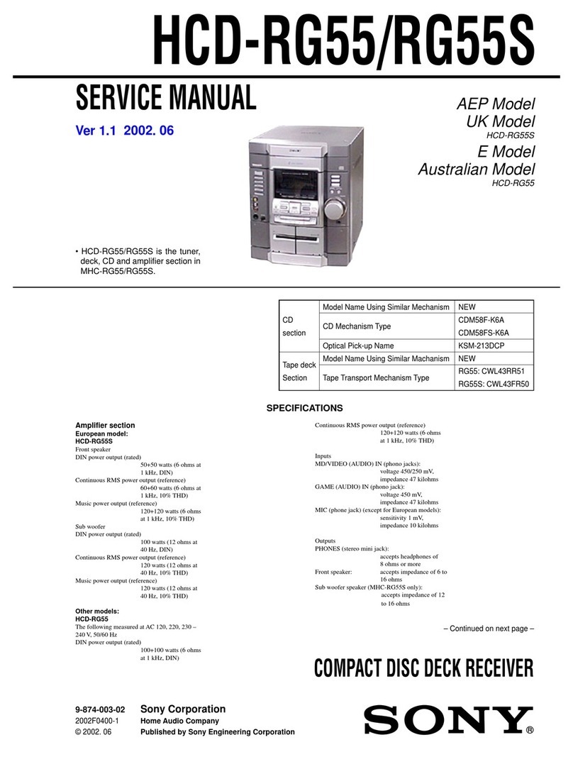
CX-LFA500 is the Amplifier, CD player, Tape
Deck and Tuner section in XR-FA500.
SPECIFICATIONS
Ver. 1.4 2005. 10
Model Name Using Similar Mechanism NEW
CD CD Mechanism Type CDM55A-K6BD44B
Section Base Unit Name BU-K1BD44B
Optical Pick-up Name KSM-213D
TAPE Model Name Using Similar Mechanism NEW
Section Tape Transport Mechanism Type CMAL1Z222B
TUNER
FM tuning range 87.5 MHz to 108 MHz
(50 kHz step)
FM usable sensitivity (IHF) 16.8 dBf
FM antenna terminal 75 (unbalanced)
AM tuning range
AM usable sensitivity 350 μV/m
AM antenna Loop antenna
AMPLIFIER
Power output Rated: 16 W + 16 W(6 ohms, T.H.D.
1 %, 1 kHz/DIN 45500)
Reference: 20 W + 20 W(6 ohms,
T.H.D. 10 %, 1 kHz/DIN 45324)
MUSIC POWER
40 W + 40 W
Input AUX IN: 500 mV
Outputs SPEAKERS: 6 ohms or more
PHONES: 32 ohms or more
European model: 531-1,602 kHz
(with the tuning interval set at 9 kHz)
Other models: 530-1,710 kHz
(with the tuning interval set at 10 kHz)
531-1,602 kHz
(with the tuning interval set at 9 kHz)
CASSETTE DECK
Track format 4 tracks, 2 channels stereo
Frequency response 50 Hz – 10000 Hz
Recording system AC bias
Heads Recording/playback ×1, erase ×1
CD PLAYER
Laser Semiconductor laser (= 780 nm)
Emission duration: continuous
D/A converter 1 bit dual
Signal-to-noise ratio 80 dB (1 kHz, 0 dB)
Wow and flutter Unmeasurable
— Continued on next page —

2
CX-LFA500
1. SERVICING NOTES ······················································· 3
2. GENERAL ·········································································· 5
3. DISASSEMBLY
3-1. Top Cabinet, Rear Panel·················································· 7
3-2. Front PanelAssy ····························································· 8
3-3. CONTROL Board, Single Cassette Mechanism·············8
3-4. CD Mechanism Deck (CDM55A-K6BD44B)················ 9
3-5. MAIN Board, POWER Board ········································ 9
3-6. LOADING Board·························································· 10
3-7. CD Board ······································································ 10
3-8. Tray (CDM55D) ··························································· 11
3-9. Optical Pick-up (KSM-213D), Holder (C213) ············· 11
4. MECHANICAL ADJUSTMENTS ····························· 13
5. ELECTRICAL ADJUSTMENTS ······························· 14
6. DIAGRAMS······································································ 17
6-1. Block Diagram – CD Section – ··································· 18
6-2. Block Diagram – Main Section – ································ 19
6-3. Printed Wiring Board – CD Section – ························· 20
6-4. Schematic Diagram – CD Section – ···························· 21
6-5. Printed Wiring Boards – Main Section – ·····················22
6-6. Schematic Diagram – Main Section – ························· 23
6-7. Printed Wiring Board – Control Section –··················· 24
6-8. Schematic Diagram – Control Section –······················ 25
6-9. Printed Wiring Board – Power Section – ·····················26
6-10. Schematic Diagram – Power Section –······················ 26
6-11. IC Pin Function Description ······································· 30
7. EXPLODEDVIEWS
7-1. Overall Section ····························································· 32
7-2. Front Section································································· 33
7-3. Chassis Section ····························································· 34
7-4. CD Mechanism Deck Section······································· 35
7-5. Optical Pick-up Section (KSM-213D)·························· 36
8. ELECTRICAL PARTS LIST······································· 37
TABLE OF CONTENTS
Ver 1.2 2003.11
GENERAL
Power requirements
European model:
Singaporeand
Australian models:
Korean model:
Taiwan model:
Other models:
Power consumption
European model:
Other models:
230 V AC, 50/60 Hz
Power consumption in standby mode
with ECO mode on: 0.3 W
with ECO mode off: 10 W
Dimensions (w/h/d) Approx. 190 ×250 ×284 mm
Mass Approx. 3.7 kg
Supplied accessories: FM antenna (1)
AM antenna (1)
Speaker cords (2)
Remote commander (1)
Batteries (2)
Specifications and external appearance are subject to change
without notice.
220-240 V AC, 50/60 Hz
220 V AC, 60 Hz
110-120 V AC, 50/60 Hz
110-120 V/220-240 V AC, 50/60 Hz
52W
60W
220 V + 240 V AC, 50/60 Hz

3
CX-LFA500
SECTION 1
SERVICING NOTES
SAFETY-RELATED COMPONENT WARNING!!
COMPONENTS IDENTIFIED BY MARK 0OR DOTTED LINEWITH
MARK 0ON THE SCHEMATIC DIAGRAMS AND IN THE PARTS
LIST ARE CRITICAL TO SAFE OPERATION. REPLACE THESE
COMPONENTS WITH SONY PARTS WHOSE PART NUMBERS
APPEAR AS SHOWN IN THIS MANUAL OR IN SUPPLEMENTS
PUBLISHED BY SONY.
CAUTION
Use of controls or adjustments or performance of procedures
other than those specified herein may result in hazardous
radiation exposure.
This appliance is classified as a CLASS 1 LASER product.
The CLASS 1 LASER PRODUCT MARKING is located on
the exterior.
Laser component in this product is capable of emitting radiation
exceeding the limit for Class 1.
The laser diode in the optical pick-up block may suffer electrostatic
break-down because of the potential difference generated by the
charged electrostatic load, etc. on clothing and the human body.
During repair, pay attention to electrostatic break-down and also
use the procedure in the printed matter which is included in the
repair parts.
The flexible board is easily damaged and should be handled with
care.
NOTES ON LASER DIODE EMISSION CHECK
The laser beam on this model is concentrated so as to be focused on
the disc reflective surface by the objective lens in the optical pick-
up block. Therefore, when checking the laser diode emission,
observe from more than 30 cm away from the objective lens.
LASER DIODE AND FOCUS SEARCH OPERATION
CHECK
Carry out the “S curve check” in “CD section adjustment” and check
that the S curve waveforms is output three times.
NOTES ON HANDLING THE OPTICAL PICK-UP
BLOCK OR BASE UNIT
Notes on chip component replacement
• Never reuse a disconnected chip component.
• Notice that the minus side of a tantalum capacitor may be dam-
aged by heat.
Flexible Circuit Board Repairing
• Keep the temperature of the soldering iron around 270 ˚C during
repairing.
• Do not touch the soldering iron on the same conductor of the
circuit board (within 3 times).
• Be careful not to apply force on the conductor when soldering or
unsoldering.

4
CX-LFA500
Service Position of the CD Mechanism Deck
Service Position of theTape Cassette Mechanism Deck

5
CX-LFA500
SECTION 2
GENERAL This section is extracted
from instruction manual.
5
PARTS AND CONTROLS
Main unit: front
Refer to the pages indicated in parentheses for details.
1
4
2
3
6
7
8
9
5
1POWER 6STANDBY/ON (7)
Switches the uniton and off (standby).
ECO (7)
Sets the ECO mode on or off.
RDS (10-12)
Activates RDS features.
2PHONES jack
Plug in optionalheadphones setwith a stereo mini plug
(ø3.5mm). Speaker output is cancelled.
3SYNCHRO REC (15)
Starts recording and CD play simultaneously.
wREC START/REC PAUSE (15)
Starts and pauses recording.
4BASS (13)
Adjusts the bass level.
TREBLE (13)
Adjusts the treble level.
5ECD (7-9)
Starts and pauses CD play.
TUNER/BAND (7, 10)
Selects tuner function and the tuner band.
dTAPE (REC MUTING) (7, 14, 15)
Starts playback and changes the playback side.
Also used to enter 4-second blankspaces during
recording.
AUX (7)
Selects the function ofexternalequipmentconnected to
AUXIN jacks.
6zOPEN/CLOSE (8)
Opens or closes the disccompartment.
7sSTOP (8, 9, 14, 15)
CD and Tape: stops playback.
f/r-,+t/g(8, 10, 12-14, 16,
17)
CD: skips to a previous or a succeeding track when
pressed,searches a track in fastforward or reverse
playback when held down.
Tape: rewinds or fastforwards the tape.
Tuner: manually tunes up or down within the band.
8zPUSH EJECT (14, 15)
Opens or closes the cassette holder.
9VOLUME (13, 16)
Adjusts the volume.
Main unit: rear
Refer to the pages indicated in parentheses for details.
1
2
3
4
5
1AM LOOP terminal and FM 75 Ωterminal
(4)
Plug in the supplied AM and FM antennas.
2AUX IN jacks
Accept analogue sound signals from externalequipment.
Connect externalequipmentusing an optionalconnecting
cable with RCA phono plugs (red plug to R jack, white
plug to L jack). Refer also to the operating instructions
for your equipment.
To switch function to externalinput, press AUX.
To changea sourcenamein thedisplay of the
AUXfunction.
Hold down AUXand press POWER while the power is
on.
AUX VIDEO TV
3SUB WOOFER3jack
Connect optionalpowered sub woofer with a built-in
amplifier to the jack.
4SPEAKERS3terminals (4)
Connect the speaker cords ofthe supplied speakers.
5AC power cord (4)
6
Remote commander
Refer to the pages indicated in parentheses for details.
1
4
5
6
7
9
8
!
@
#
0
2
3
Buttons with the same or similar names on the main unit
basically have the same function.
1POWER (7)
21–10/0, >10 (8, 10)
CD: selects a track ofthe specified number.
Tuner: tunes in the station with the specified preset
number.
The numbered buttons take on these functions when pressed with
SHIFT held down
:
CLOCK (7)
Selects clock mode.
TIMER (16)
Selects timer mode.
TUNER MODE (13)
Switches between stereo or monauralFM reception.
REV MODE (14, 15)
Selects a reverse mode.
3SHUFFLE/PROGRAM (8, 9)
Selects shuffle or programmed CD playback mode.
REPEAT (8)
Selects repeatCD playback mode.
4PRESETN,M(10)
f/r,t/g(8, 10, 12-14, 16, 17)
ENTER (7, 10, 16, 17)
Determines the mode.
Stores the received station to preset.
5ECD (7-9)
TUNER/BAND (7, 10)
dTAPE (7, 12)
AUX (7)
6DISPLAY (8)
Changes the display in CD playback mode.
DIMMER (7)
Adjusts the display windowbrightness.
SLEEP (16)
Selects sleep-timer mode.
7SHIFT
Hold down when pressing a numbered button to change
its function to thatprinted above the number.
8MUTING (13)
To turn off the sound temporarily.
9CLEAR (9, 10, 17)
CD: Clears a CD program
Tuner: Clears a presetstation.
0TREBLE (13)
BASS (13)
!s(8, 9, 14, 15)
@FUNCTION (15)
Switches the active function among TAPE,TUNER,AUX
(VIDEO or TV) and CD.
#VOLUME +,-(13)
6
CX-LFA500
7
ADJUSTMENTS BEFORE OPERATION
ECO CLOCK
POWER
DIMMER
SHIFT
ECD,
TUNER/
BAND,
dTAPE,
AUX
f,g
POWER
6STANDBY/ON
ECD,
TUNER/
BAND,
dTAPE,
AUX
ENTER
f,g
ECO mode
Reduces power consumption in standby mode with the following
operations.
Press ECO.
Each press ofthe button changes the mode as follows;
ECO ON:Power economizing mode is activated.
When the unitturns off, everything in the display disappears
and only the red indicator above POWER lights to showthat
the power is being supplied.
ECO OFF:Power economizing mode is cancelled.
When the unitturns off, the clock display appears.
Initialmode is ECO OFF.
Standby power consumption
ECO ON: 0.3W
ECO OFF: 10 W
Setting the clock
1
In stop mode, hold down SHIFT and press CLOCK
on the remote.
Go to step3when the hour ofthe clock display flashes.
2
Within 6 seconds, press ENTER.
The hour flashes in the display.
3
Press for gto set the hour, then press
ENTER.
4
Press for gto set the minute.
Each press changes the time in 1-minute steps.
5
Press ENTER.
The time display stops flashing and the clock starts from
00 seconds.
To display thetimewhilethepower is on
Hold down SHIFT and press CLOCK on the remote.
The time will be displayed for 6 seconds.
Tip:
''AM 12:00" indicates midnight and "PM12:00" noon.
If "- -:- -" appears when theunit is turned off
There has been a power interruption. Resetthe clock.
Power
Turning theunit on
Press POWER 6STANDBY/ON(POWER on the remote ).
Alternatively,press dTAPE,TUNER/BAND,AUXor
ECD. Playback will startautomatically ifa discor tape is
loaded.
Turning theunit off
Press POWER 6STANDBY/ONagain.
The unitgoes into standby.
Dimmer
The display window brightness can be selected.
Press DIMMER on the remote repeatedly.
Each press ofthe button changes the following three levels:
"DIMMER 1","DIMMER 2" and "DIMMER 0".
"DIMMER 0" is brightest.

7
CX-LFA500
SECTION 3
DISASSEMBLY
Note: Follow the disassembly procedure in the numerical order given.
• This set can be disassembled in the order shown below.
SET
MAIN BOARD,
POWER BOARD LOADING BOARD CD BOARD TRAY (CDM55D)
OPTICAL PICK-UP
(KSM-213D),
HOLDER (C213)
CD MECHANISM DECK
(CDM55A-K6BD44B) CONTROL BOARD,
SINGLE CASSETTE MECHANISM
FRONT PANEL ASSY
TOP CABINET,
REAR PANEL
3-1.Top Cabinet, Rear Panel
1
three s
crews
(+KTP 3
×
12)
2
three s
crews
(+KTP 3
×
12)
3
six s
crews
(+BVTP 3
×
10)
7
two s
crews
(+BVTP 3
×
10
)
8
three s
crews
(+BVTP 3
×
10
)
5
top cabinet
4
qa
rear panel
q;
tuner (FM/AM)
6
w
ire (flat type)
15p
a
a
b
b
9
three s
crews
(+BVTP 3
×
10)
Ver 1.2 2003.11

8
CX-LFA500
3-2. Front Panel Assy
1
two s
crews
(+KTP 3
×
12)
2
four s
crews
(+BVTP 3
×
10
)
3
w
ire (flat type) 12p (CN305)
4
w
ire (flat type) 25p (CN302)
8
front panel assy
5
connector 5p (CN1)
6
connector 6p
7
connector 5p (CN201)
3-3. CONTROL Board, Single Cassette Mechanism
7
single cassette mechanism
(CMAL1Z222B)
5
CONTROL
board
1
twelve s
crews (+BVTP 3
×
10)
6
four s
crews (+BVTP 3
×
10
)
2
w
ire (flat type) 25p (CN601)
3
w
ire (flat type) 12p (CN602)
4
w
ire (flat type) 8p (CN603)
9
CX-LFA500
3-4. CD Mechanism Deck (CDM55A-K6BD44B)
1
s
crew (+BVTP 3
×
10)
5
CD holder
4
3
s
crew (+BVTP 3
×
10)
6
CD door assy
7
CD mechanism deck
(CDM55A-K6BD44B)
2
w
ire (flat type) 21p (CN303)
3-5. MAIN Board, POWER Board
2
two s
crews (+BVTP 3
×
10
)
3
two s
crews
(+BVTP 3
×
10)
7
four s
crews
(+BVTP 3
×
10)
4
six s
crews
(+BVTP 3
×
10)
5
heat sink assy
6
MAIN board
9
POWER board
1
connector 7p (CN801)
8
power transformer

10
CX-LFA500
3-6. LOADING Board
5
LOADING board
2
two
screws (+BTP 2.6
×
6)
4
motor
(LD) assy
(M901)
1
Remove the belt.
3
Remove soldering from the two points.
3-7. CD Board
2
Remove soldering
from the four points.
3
wire (flat type) 16
p
5
CD board
4
wire (flat type) 21p (CN101)
1
screw(+P 2.6
×
5)

11
CX-LFA500
3-8.Tray (CDM55D)
2
tray
1
While pressing the two protrusions
A
and
B
to unlock the two claws as shown,
pull the tray in the direction of the arrow
C
. (Be careful of the claws.)
claw
claw
C
A
B
3-9. Optical Pick-up (KSM-213D), Holder (C213)
1
two floating
screw
s
(+PTPWH M2.6)
qf
floating
screws
(+PTPWH M2.6)
qg
holder
(C213)
5
screw (+PTTP M2.6)
6
stopper (BU)
2
two compression spring
(T213)
7
compression spring
(T213)
3
insulator
8
insulator
9
screw (+PTTP M2.6)
q;
stopper (BU)
qa
compression spring
(T213)
qs
insulator
qd
optical pick-up
(KSM-213D)
4
insulator
Ver 1.2 2003.11

12
CX-LFA500
MEMO

13
CX-LFA500
2.94 – 7.84 mN • m
(30 to 79 g • cm)
(0.42 – 1.11 oz • inch)
0.15 – 0.59 mN • m
(2 to 6 g • cm)
(0.03 – 0.08 oz • inch)
0.15 – 0.59 mN • m
(2 to 6 g • cm)
(0.03 – 0.08 oz • inch)
0.15 – 0.59 mN • m
(2 to 6 g • cm)
(0.03 – 0.08 oz • inch)
6.86 – 17.64 mN • m
(70 to 179 g • cm)
(0.98 – 2.49 oz • inch)
9.8 mN • m or more
(100 g • cm or more)
(1.4 oz • inch or more)
9.8 mN • m or more
(100 g • cm or more)
(1.4 oz • inch or more)
CQ-102C
CQ-102C
CQ-102RC
CQ-102RC
CQ-201B
CQ-403A
CQ-403R
Precaution
1. Clean the following parts with a denatured alcohol-moistened
swab:
record/playback heads pinch rollers
erase head rubber belts
capstan idlers
2. Demagnetize the record/playback head with a head demag-
netizer.
3. Do not use a magnetized screwdriver for the adjustments.
4. After the adjustments, apply suitable locking compound to the
parts adjusted.
5. The adjustments should be performed with the rated power
supply voltage unless otherwise noted.
Torque Measurement
SECTION 4
MECHANICAL ADJUSTMENTS
Mode
FWD
FWD
back tension
REV
REV
back tension
FF/REW
FWD tension
REV tension
Torque meter Meter reading

14
CX-LFA500 SECTION 5
ELECTRICAL ADJUSTMENTS
[Record/Playback Head Azimuth Adjustment]
Procedure:
1. Mode : Playback
2. Turn the adjustment screw and check output peaks. If the peaks
do not match for L-CH and R-CH, turn the adjustment screw
so that outputs match within 1 dB of peak.
test tape
P-4-A100
(10kHz,–10dB)MAINboard
J203
speaker terminal
level meter
set +
–
L-CH
peak
R-CH
peak
screw
position
output
level within
1dB
L-CH
peak
R-CH
peak
screw
position
within 1dB
Signal Used forTape
P-4-A100
WS-48B
10 kHz, –10 dB
3 kHz, 0 dB
Azimuth Adjustment
Tape Speed Adjustment
DECK SECTION 0 dB=0.775V
1. Demagnetize the record/playback head with a head demagnetizer.
2. Do not use a magnetized screwdriver for the adjustments.
3. After the adjustments, apply suitable locking compound to the
parts adjusted.
4. The adjustments should be performed with the rated power
supply voltage unless otherwise noted.
5. The adjustments should be performed in the order given in this
service manual. (As a general rule, playback circuit adjustment
should be completed before performing recording circuit
adjustment.)
6. The adjustments should be performed for both L-CH and R-
CH.
7. Switches and controls should be set as follows unless otherwise
specified.
4. After the adjustments, apply suitable locking compound to the
parts adjusted.
Adjustment Location: Record/Playback/Erase Head
[Tape Speed Check]
Procedure:
1. Turn the power on.
2. Insert the WS-48B into deck.
3. Press the Ybutton of deck.
4. Check the reading of frequency counter becomes 3000 ± 90 Hz.
Sample Value of Wow and flutter
W.RMS (JIS) less than 0.3%
(test tape: WS-48B)
3. Mode: Playback
test tape
P-4-A100
(10kHz,–10dB)
oscilloscope
set
Waveform of oscilloscope
in phase 45
°
90
°
135
°
180
°
good wrong
MAINboard
J203
speaker terminal
L
R

15
CX-LFA500
RFDC signal waveform
Checking Location: CD board (Conductor side)
RFAC Level Check
Connection:
Procedure:
1. Connect an oscilloscope to test point TP (RFAC) and TP (VC)
on the CD board.
2. Turn the power on.
3. Put the disc (YEDS-18) in to playback the number five track.
4. Confirm that oscilloscope waveform is clear and check RFAC
signal level is correct or not.
Note: A clear RFAC signal waveform means that the shape “◊” can be
clearly distinguished at the center of the waveform.
RFAC signal waveform
Checking Location: CD board (Conductor side)
CD SECTION
Note:
1. CD Block is basically designed to operate without adjustment. There-
fore, check each item in order given.
2. Use YEDS-18 disc (3-702-101-01) unless otherwise indicated.
3. Use an oscilloscope with more than 10MΩimpedance.
4. Clean the object lens by an applicator with neutral detergent when the
signal level is low than specified value with the following checks.
S-curve Check
Connection:
Procedure:
1. Connect an oscilloscope to test point TP (FE) and TP (DVC)
on the CD board.
2. Turn the power on.
3. Put the disc (YEDS-18) in and turned power switch on again
and actuate the focus search. (actuate the focus search when
disc table is moving in and out)
4. Check the oscilloscope waveform (S-curve) is symmetrical
between A and B. And confirm peak to peak level within 2 ± 1
Vp-p.
S-curvewaveform
Note: • Try to measure several times to make sure than the ratio of A : B
or B : A is more than 10 : 7.
• Take sweep time as long as possible and light up the
brightness to obtain best waveform.
Checking Location: CD board (Conductor side)
RFDC Level Check
Connection:
Procedure:
1. Connect an oscilloscope to test point TP (RFDC) and TP (DVC)
on the CD board.
2. Turn the power on.
3. Put the disc (YEDS-18) in to playback the number five track.
4. Confirm that oscilloscope waveform is clear and check RFDC
signal level is correct or not.
Note: A clear RFDC signal waveform means that the shape “◊” can be
clearly distinguished at the center of the waveform.
+
–
CD board
TP (FE)
TP (DVC)
oscilloscope
A
B
symmetry
within 2
±
1Vp-p
+
–
CD board
TP (RFDC)
TP (DVC)
oscilloscope
VOLT/DIV: 200 mV
TIME/DIV: 500 ns
level: 0.7
±
0.2 Vp-p
+
–
CD board
TP (RFAC)
TP (VC)
oscilloscope
VOLT/DIV: 200 mV
TIME/DIV: 500 ns
level: 0.9
±
0.4 Vp-p

16
CX-LFA500
E-F Balance Check
Connection:
Procedure:
1. Connect an oscilloscpe to test point TP (TE) andTP (DVC) on
the CD board.
2. AC is put in pushing CD ubutton.
3. FL tube carries out all lights and goes into CD test mode.
4. Put the disc (YEDS-18) in to playback the number five track.
5. Press the CD ubutton. (The tracking servo and the sledding
servo are turned OFF)
6. Check the level B of the oscilliscope's waveform and the A
(DC voltage) of the center of the Traverse waveform.
Confirm the following :
A/B x 100 = less than ± 22%
Traverse Waveform
7. Press the CD ubutton. (The tracking servo and sledding
servo are turned ON)
Confirm the C (DC voltage) is almost equal to the A (DC
voltage) is step 4.
8. To exit from this mode, turn the power off.
Notes: • Always move the optical pick-up to most inside track when
exiting from this mode. Otherwise, a disc will not be unloaded.
• Do not run the sled motor excessively, otherwise the gear can
be chipped.
Traverse Waveform
Checking Location: CD board (Conductor side)
+
–
CD board
TP (TE)
TP (DVC)
oscilloscope
0V
B
level: 1.15
±
0.5 Vp-p
Center of
the waveform
A (DC
voltage)
0V
Tracking servo
Sled servo
ON
C (DC
voltage)
Tracking servo
Sled servo
OFF
Checking Location:
– CD BOARD (Conductor Side) –
TP (VC)
TP (FE)
TP (TE) TP
(RFDC)
TP
(DVC)
TP
(RFAC)
IC103
IC101

1717
CX-LFA500
SECTION 6
DIAGRAMS
• Circuit Boards Location
THIS NOTE IS COMMON FOR PRINTED WIRING
BOARDS AND SCHEMATIC DIAGRAMS.
(In addition to this,the necessary note is printed
in each block.)
For schematic diagrams.
Note:
• All capacitors are in µF unless otherwise noted. pF: µµF
50 WV or less are not indicated except for electrolytics
and tantalums.
• All resistors are in Ωand 1/4W or less unless otherwise
specified.
•f: internal component.
•2: nonflammable resistor.
•1: fusible resistor.
•C: panel designation.
For printed wiring boards.
Note:
•X: parts extracted from the component side.
•Y: parts extracted from the conductor side.
•f: internal component.
•: Pattern from the side which enables seeing.
•A: B+ Line.
•B: B– Line.
• VoltagesaretakenwithaVOM (Input impedance 10 MΩ).
Voltage variations may be noted due to normal produc-
tion tolerances.
• Waveforms are taken with a oscilloscope.
Voltage variations may be noted due to normal produc-
tion tolerances.
• Circled numbers refer to waveforms.
• Signal path.
F:TUNER
J: CD
d: AUX
E: PB (TAPE)
a: REC (TAPE)
Note: The components identified by mark 0or dotted line
with mark 0are critical for safety.
Replace only with part number specified.
• Indication of transistor
C
BThese are omitted.
E
Q
B
These are omitted.
CE
• Waveforms
– CD Board –
1.1Vp-p
1IC103 qg (RFAC)
(CD Play Mode)
2IC101 el (FE)
(CD Play Mode)
200mV/DIV,
1
μ
s
/DIV
50mV/DIV,
200
μ
s
/DIV
100mV/DIV,
200
μ
s
/DIV
1V/DIV,
20ns
/DIV
200mVp-p
250mVp-p
3IC101 ra (TE)
(CD Play Mode)
4IC101 yj (XTAO)
5.4Vp-p
59ns
MAIN BOARD
CD BOARD
LOADING BOARD
PHONE BOARD
CONTROL BOARD
POWER BOARD
6IC601 qh (XOUT)
1V/DIV,
40ns
/DIV
1V/DIV,
20
μ
s
/DIV
5IC601 qd (O-XT2)
5.5Vp-p
30.5
μ
s
2.7Vp-p
116ns
7Q301
collector (Rec mode)
5V/DIV,
4
μ
s
/DIV
11.8Vp-p
11.7
μ
s
– FRONT Board – – MAIN Board –

1818
CX-LFA500
6-1. Block Diagram – CD Section –
: CD
• SignalPath
SQSO
SQCK
A/D
CONVERTER
CH1OUTF
CH1OUTR
6
7
8
9
16
18
11
10
12
2
1
51
49
48
43
24
41
40 39
64 15
28
29
30
31
32
33
24
25
23
5
6
2
3
17
18
15
16
E
B
C
D
A
CD +5V
F
DETECTOR
A
B
C
D
RF
SUMMING
AMP
FOCUS
ERRORAMP
TRACKING
ERRORAMP
RFAC
FE
IC103
RF AMP,
FOCUS/TRACKING ERRORAMP
TE
E
FFI-V AMP
E I-V AMP
Q101
AUTOMATIC
POWER
CONTROL
APC LD
AMP
LD
LD
PD
LASERDIODE
RFAC
ASYO
ASYI
ASYMMETRY
CORRECTION
DIGITAL
PLL
IC101 (1/2)
DIGITAL SIGNAL PROCESSOR,
DIGITAL FILTER, D/A CONVERTER
DATA
XLAT
CLOK
14 56
MDP
26 7 8
XLON
3
XRST
DIGITAL
CLV
D/A
INTERFACE
SE
TE
FE
RFDC
FOCUS/TRACKING/SLED
SERVO DSP
FOCUS/TRACKING/SLED
PWM GENERATOR
SFDR
CH3FIN
CH4SIN
CH3RIN
CH3OUTF
CH3OUTR
CH2FIN
CH2RIN
CH1FIN
CH1RIN
20
MUTE
SRDR
TFDR
TRDR
FFDR
FRDR
S101
(LIMIT)
EMPH
WFCK
GFS
MIRR/DFCT/
FOK
DETECTOR
SERVO AUTO
SEQUENCER
SERVO
INTERFACE
CPU INTERFACE
18
63
62
61
19
SENS
20
86
97
87
94 3
SCOR
C-SQSO
C-SQCK
C-XLT
C-CLK
C-DATA
C-SENS
C-SCOR
1 2
96 88
SCLK
COUT
921
SSTP
27
FOK
22
23
MIRR
DFCT
TO SERVO INTERFACE
CH4OUTF
CH4OUTR
(SPINDLE) MOTOR
DRIVE
MOTOR
DRIVE
CH2OUTF
CH2OUTR
M
M
(SLED)
IC102
FOCUS/TRACKING COIL DRIVE,
SPINDLE/SLED MOTORDRIVE
2-AXIS
DEVICE
(TRACKING)
(FOCUS)
IC101 (2/2)
DIGITAL SERVO
PROCESSOR
OPTICAL PICK-UP
BLOCK
KSM-213D
SW
PD
I-V AMP
12
11
13
14
54 56 53 55
FILTER
FILO
PCO
CLTV
FILI
EFM
DEMODULATOR
SERIAL
IN
INTERFACE
DIGITAL
FILTER,
NOISE SHAPER
PWM
&
INTEGRATOR
BUFFER
CLOCK
GENERATOR
TIMING
LOGIC
DIGITAL
OUT
INTERNAL BUS
16K
RAM
ERROR
CORRECTOR
SUBCODE
PROCESSOR
60
85 C-XRST
XTAI
X101
16.9344MHz
AIN1
AIN2
AOUT1
AOUT2
TO MIRR/DFCT/
FOKDETECTOR
PCMD
BCK
LRCK
C2PO
DOUT
66
XTAO 67
70
77
LOUT1
LOUT2R-CH
72
75
71
76
A
MAIN SECTION
EQ
IN 15
3
4EQ
AC
SUM
17
FEI
RF DC
AMP 28
RFDCO
29
RFDCI
COIL
DRIVE
COIL
DRIVE
2
1
C-PWM2
C-PWM1
PWM3
PWM2
PWM3
PWM2
95 C-LD ON
IC601 (1/2)
CD
L-CH
RFAC
VCA
+7V
+7V
+5V
SYSTEMCONTROLLER
+3.3V
REG
Q102
CD +5V
REG
Q419
Ver 1.2 2003.11

1919
CX-LFA500
6-2. Block Diagram – Main Section –
: TUNER
: CD
• SignalPath
• R-CHis omitted dueto same as L-CH.
: AUX
: PB (TAPE)
: REC (TAPE)
R-CH
BIAS
OSC
Q301
Q302
+VM
ERASE
HEAD
REC/PB
HEAD
DECK
Q609
PB
SWITCH
RCOUNT
99
RCLK
100
RCE
84
SYSTEMCONTROLLER
IC601(2/2)
RDATA
98
L
R
AUX
J201
MUTE CONT
Q263
J601
HEADPHONES
RCH
RCH
L
R
L
R
FUCTION
KEY
REMOTE
CONTROL
RECEIVER
IC602
S601-607
D603
ECO
TUNER UNIT
L-CH
R-CHR-CH
D OUT
D IN
CLK
CE
TUNED
R-CH
RTUNED
93
Q310,311
REC
SWITCH
Q305,306,307
L301
REC BIAS
Q303
Q304
MECHA BLOCK
SW1
PLAY
TSOL
DRIVE
Q608
MOTOR
DRIVE
Q606
TREC
77
BIAS
81
TSW
24
XT1
12
XT2
13
X601
32.768kHz
X IN
15
X OUT
16
X602
8.64MHz
MUTE
Q261
9PAMP MUTE
Q221,253
Q214,216-220
Q223,225,229
29
RMC
FUCTION
KEY
S608-613
19
KEY2
BASE
ENCODER
S614
20
BASE ENC
75
LED CONT
31
RESET
SWITCH
Q601
11
RESETRESET
IC603
21
D610
25
SHDET
D801-804
RELAY
DRIVE
AC
IN
PT802
ECO
CD POWER
CONTROL
Q420
Q401 RY801
18
KEY1
82CD FU
REG
Q312
+10V
+5V
+VM
PB/REC EQ AMP
IC301
AUX L
19 18
OUTL
TU L
23
TAPE L
2
CD L
21
16
OUTRR-CH
13
CONT
28
REC OUT
RMUTE
80
RDS SIG
23
RDS DATA
91
RST
92
STEREO
MUTE
FM SOUT
RDATA
RINT RDS CLK
27
R-CH
R-CH
SW2
RREC
SW3
FREC
SW4
PACK
SW5
PEND
M
M1
DECK
MOTOR
L OUT2R-CH
L OUT1
FDATA
10
TPLAY SW
79
TMTR CONT
6
TEND SW
5
TSOL
4
MOTORDRIVE
IC604
OUT1
4 7
FIN
OUT2
2 9
RIN
OPEN
M
TRY
MOTOR
CLOSE
CD OPEN/CLOSE
28 CD DOORSE
74 OPEN
73 CLOSE
Q222
DC
DET
PRE
AMP
POWER
AMP
RCH
J203
SPEAKERS
45
47
50
.
52
66
.
SEG1
SEG20
34
45
GRID1
GRID11
FLUORESCENT
DISPLAY
FL601
FIL1 FIL2
TREBLE
ENCODER
S615
21TREBLE ENC
VOLUME
ENCODER
S616
22
VOL ENC
POWER
CONTROL
D602
+5V
REG
Q602-604
μCON+B
V ECO
D608
POWER
SWITCH
8
PCONT
Q605
Q610
LINE
FILTER
L801
V ECO
PT801
POWER
TRANS
FIL2
FIL1
D402
D404-407
2 TIMES
DET
D409,410
-VFL
REG
Q413
-VFL
-VP
+VP
+7V
REG
Q416-418
+7V
+VM
REG
Q402,403,405
+VM
+VCC
REG
Q406,407
+VCC D417
AC
DET
Q412
DC
DET
Q408,409
HOLD
Q411
OVER
CURRENT
DET
Q201,243
25
HOLD
L-CH
A
CD SECTION

2020
CX-LFA500
6-3. PrintedWiring Board – CD Section –
IC102
IC101
IC103
TP (VC)
TP (RFAC)
TP (DVC)
CN303
22
1-680-849-
()
12
A
B
C
D
E
F
G
345678
Ref. No. Location
D101 F-5
IC101 E-4
IC102 C-5
IC103 D-2
Q101 C-2
Q102 G-5
• Semiconductor
Location
• See page 17 for Circuit Boards Location.
Ver 1.2 2003.11
Table of contents
Other Sony Stereo System manuals

Sony
Sony SAV-E525 User manual

Sony
Sony CMT-SBT20B User manual

Sony
Sony MHC-RV6/RV5 User manual

Sony
Sony LBT-XG60 User manual

Sony
Sony HCD-XGV80 User manual

Sony
Sony HCD-DP800AV User manual

Sony
Sony LBT-DR5 User manual

Sony
Sony SA-WMS556 User manual

Sony
Sony ZS-2000 Primary User manual

Sony
Sony HCD-VX880AV User manual

Sony
Sony MHC-W550 User manual

Sony
Sony HCD-EX1 User manual

Sony
Sony MHC-V43D Reference guide

Sony
Sony ICF-CS15IPBLKN User guide

Sony
Sony SS-CEP515 User manual

Sony
Sony Muteki LBT-ZX66i User manual

Sony
Sony HCD-ZUX9 User manual

Sony
Sony MHC-WZ8D User manual

Sony
Sony CMT-LS1 - Micro Hi Fi Component System User manual

Sony
Sony LBT-G3000 User manual