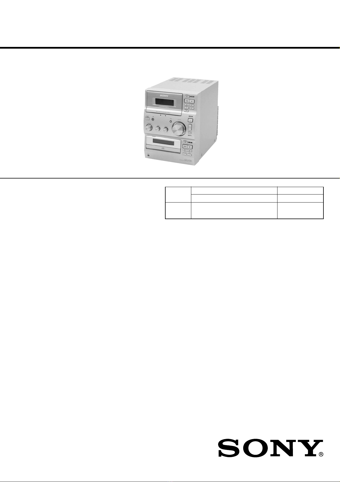
Sony HCD-CP100 User manual

SERVICE MANUAL
9-873-802-11 Sony Corporation
2001B0500-1 Audio Entertainment Group
C2001.2 General Engineering Dept.
Ver 1.0 2001.02
MICRO HiFi COMPONENT SYSTEM
CMT-CP100/CP100K
CMT-CP100 CMT-CP100K
COMPACT DISC DECK HCD-CP100 HCD-CP100K
RECEIVER SYSTEM
SPEAKER SYSTEM SS-CCP500
US Model
Canadian Model
AEP Model
UK Model
Australian Model
CMT-CP100
E Model
CMT-CP100/CP100K
SPECIFICATIONS
• CMT-CP100/CP100K are composed of following models.
As for the service manual, it is issued for each component model,
then, please refer to them.
COMPONENT MODEL NAME
ACCESSORIES & PACKING MATERIALS
********************************
1-476-663-11 REMOTE COMMANDER (RM-SCP100)
1-501-374-11 ANTENNA, LOOP (CP100)
1-501-659-61 ANTENNA (FM) (US, CND, E, EA, TH, AR)
1-754-060-11 ANTENNA (FM) (AEP, UK, MX, AUS/CP100K)
1-754-153-11 ANTENNA, LOOP (CP100K)
4-230-866-01 COVER (BATTERY) (for RM-SCP100)
4-233-754-11 MANUAL, INSTRUCTION (ENGLISH)
(US, CND, AEP, UK, E, EA, SP, TH, AR, AUS)
4-233-754-21 MANUAL, INSTRUCTION (FRENCH, SPANISH)
(AEP, E, SP)
4-233-754-31 MANUAL, INSTRUCTION (FRENCH) (US, CND, EA)
4-233-754-41 MANUAL, INSTRUCTION (SPANISH) (MX, AR)
4-233-754-51 MANUAL, INSTRUCTION
(GERMAN, DUTCH, ITALIAN, SWEDISH, POLISH) (AEP)
4-233-754-61 MANUAL, INSTRUCTION (ARABIC) (EA)
4-233-754-71 MANUAL, INSTRUCTION (TRADITIONAL CHINESE)
(SP, TH)
4-233-755-11 MANUAL, INSTRUCTION (DANISH, FINNISH) (AEP)
4-233-755-21 MANUAL, INSTRUCTION (PORTUGUESE) (AEP)
4-233-755-31 MANUAL, INSTRUCTION (RUSSIAN) (AEP)
4-233-756-11 MANUAL, INSTRUCTION (KOREAN) (CP100K)
PARTS LIST
Part No. Description Remark
•Abbreviation
AR : Argentina model
AUS : Australian model
CND : Canadian model
EA : Saudi Arabia model
MX : Mexican model
SP : Singapore model
TH : Thailand model
Power requirements
North American model: 120 V AC, 60 Hz
European model: 230 V AC, 50/60 Hz
Australian model: 220 - 240 V AC, 50/60 Hz
Mexican model: 120 V AC, 60 Hz
Other models: 110 - 120 V or 220 -
240 V AC , 50/60 Hz
Adjustable with voltage
selector
Power consumption
European model: See the nameplate
0.5 W (in the standby
mode)
Other models: See the nameplate
Dimensions (w/h/d) Approx. 190 ×252 ×
345 mm incl. projecting
parts and controls
Mass Approx. 5.6 kg
Supplied accessories Remote commander (1)
AM loop antenna (1)
FM wire antenna (1)
Batteries (2)
Design and specifications are subject to change
without notice.

SERVICE MANUAL
MICRO Hi-Fi COMPONENT SYSTEM
US Model
Canadian Model
AEP Model
UK Model
Australian Model
HCD-CP100
E Model
HCD-CP100/CP100K
SPECIFICATIONS
HCD-CP100/CP100K
Ver 1.0 2001.02
9-873-803-11 Sony Corporation
2001B0500-1 Audio Entertainment Group
C2001.2 General Engineering Dept.
HCD-CP100/CP100K is the Amplifier, CD
player, Tape Deck and Tuner section in
CMT-CP100/CP100K.
– Continued on next page –
Model Name Using Similar Mechanism NEW
CD Mechanism Type CDM55F-K6BD41A
Model Name Using Similar Mechanism NEW
CD
Section
Tape deck
Section
Amplifier section
For the U.S. model
AUDIO POWER SPECIFICATIONS
POWER OUTPUT AND TOTAL
HARMONIC DISTORTION:
With 6-ohm loads, both channels driven, from
70 - 20,000 Hz; rated 18 watts per channel
minimum RMS power, with no more than 0.9%
total harmonic distortion from 250 milliwatts to
rated output.
North American model:
Continuous RMS power output (reference):
35 + 35 W
(6 ohms at 1 kHz, 10%
THD)
Total harmonic distortion less than 0.07% (6 ohms at
1 kHz, 18 W)
European model:
DIN power output (rated): 30 + 30 W
(6 ohms at 1 kHz, DIN)
Continuous RMS power output (reference):
35 + 35 W
(6 ohms at 1 kHz, 10%
THD)
Music power output (reference):
85 + 85 W
Other models:
The following measured at 230 V AC, 60 Hz
DIN power output (rated): 27 + 27 W
(6 ohms at 1 kHz, DIN)
Continuous RMS power output (reference):
32 + 32 W
(6 ohms at 1 kHz, 10%
THD)
The following measured at 220 V AC, 60 Hz
DIN power output (rated): 23 + 23 W
(6 ohms at 1 kHz, DIN)
Continuous RMS power output (reference):
26 + 26 W
(6 ohms at 1 kHz, 10%
THD)
Inputs
AUDIO IN MD (VIDEO) (phono jacks):
Sensitivity 500/250 mV,
impedance 47 kilohms
Outputs
OPTICAL DIGITAL OUT (CD):
Optical
PHONES (stereo phone jack):
Accepts headphones with
an impedance of 8 ohms
or more
SPEAKER: Active speaker system,
6 ohms

2
HCD-CP100/CP100K
CD player section
System Compact disc and digital
audio system
Laser Semiconductor laser
(λ= 780 nm)
Emission
duration: continuous
Wavelength 780 - 790 nm
Frequency response 2 Hz - 20 kHz (±0.5 dB)
Tape player section
Recording system 4-track 2-channel stereo
Frequency response 50 - 13,000 Hz (±3 dB),
using a Sony TYPE I
cassette
Wow and flutter ±0.15% W. Peak (IEC)
0.1% W. RMS (NAB)
±0.2% W. Peak (DIN)
Tuner section
FM stereo, FM/AM superheterodyne tuner
FM tuner section
Tuning range
North American model: 87.5 - 108.0 MHz
(100-kHz step)
Other models: 87.5 - 108.0 MHz
(50-kHz step)
Antenna FM wire antenna
Antenna terminals 75 ohm unbalanced
Intermediate frequency 10.7 MHz
AM tuner section
Tuning range
Pan-American model: 530 - 1,710 kHz
(with the tuning interval
set at 10 kHz)
531 - 1,710 kHz
(with the tuning interval
set at 9 kHz)
European model: 531 - 1,602 kHz
(with the tuning interval
set at 9 kHz)
Middle Eastern and Philippine models:
531 - 1,602 kHz
(with the tuning interval
set at 9 kHz)
Other models: 530 - 1,710 kHz
(with the tuning interval
set at 10 kHz)
531 - 1,602 kHz
(with the tuning interval
set at 9 kHz)
Antenna AM loop antenna, external
antenna terminal
Intermediate frequency 450 kHz
General
Power requirements
North American model: 120 V AC, 60 Hz
European model: 230 V AC, 50/60 Hz
Australian model: 220 - 240 V AC, 50/60 Hz
Mexican model: 120 V AC, 60 Hz
Other models: 110 - 120 V or 220 -
240 V AC , 50/60 Hz
Adjustable with voltage
selector
Power consumption
European model: See the nameplate
0.5 W (in the standby
mode)
Other models: See the nameplate
Dimensions (w/h/d) Approx. 190 ×252 ×
345 mm incl. projecting
parts and controls
Mass Approx. 5.6 kg
Design and specifications are subject to change
without notice.
TABLE OF CONTENTS
1. SERVICING NOTES ............................................... 4
2. GENERAL
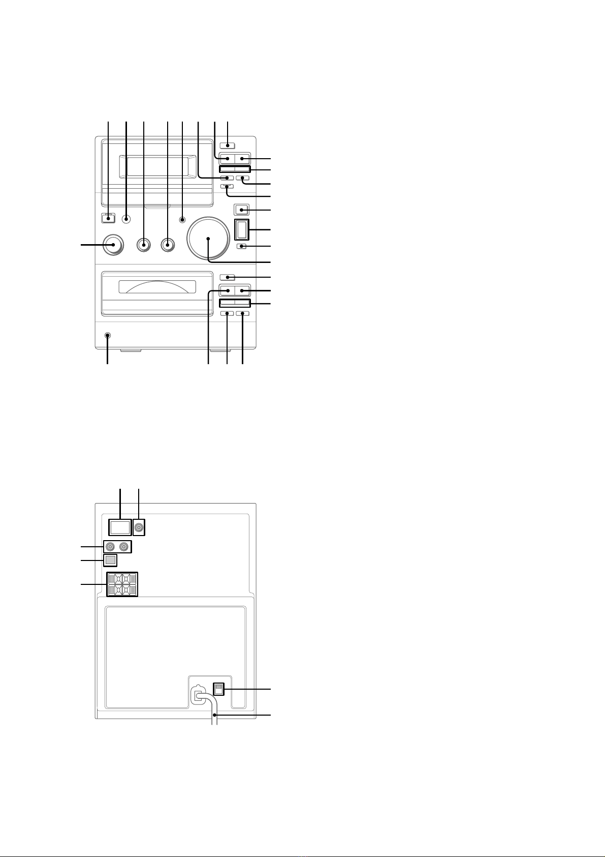
Location of Controls ....................................................... 5
Setting the Time .............................................................. 6
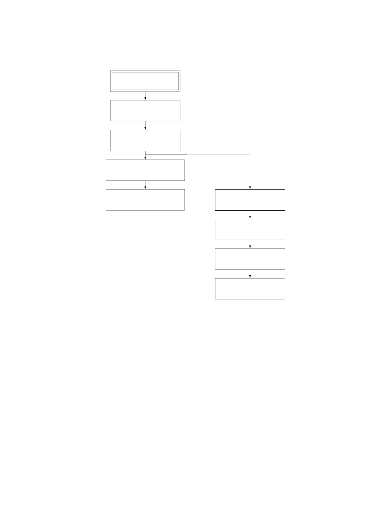
3. DISASSEMBLY
3-1. Disassembly Flow ........................................................... 7
3-2. Cover (Upper) ................................................................. 8
3-3. CD Lid ............................................................................. 8
3-4. Front Panel Section ......................................................... 9
3-5. Tape Mechanism Deck.................................................... 9
3-6. CD Mechanism Deck (CDM55F-K6BD41A)................ 10
3-7. Base Unit (BU-K6BD41A)............................................. 10
3-8. Loading Board................................................................. 11
3-9. Cam (CDM55) ................................................................ 11
4. TEST MODE.............................................................. 12
5. ELECTRICAL ADJUSTMENTS
Deck Section ................................................................... 13
CD Section ...................................................................... 13
6. DIAGRAMS
6-1. Block Diagram – CD SERVO Section – ........................ 14
6-2. Block Diagram – MAIN Section – ................................. 15
6-3. Block Diagram
– DISPLAY/POWER SUPPLY Section – ...................... 16
6-4. Note for Printed Wiring Boards and
Schematic Diagrams ....................................................... 17
6-5. Printed Wiring Board – CD Board – .............................. 18
6-6. Schematic Diagram – CD Board – ................................. 19
6-7. Printed Wiring Board – TC Board – ............................... 20
6-8. Schematic Diagram – TC Board –.................................. 21
6-9. Schematic Diagram
– MAIN (1/2)/LOADING Board – ................................. 22
6-10. Schematic Diagram – MAIN Board (2/2) – ................... 23
6-11. Printed Wiring Board – MAIN Board – ......................... 24
6-12. Printed Wiring Boards
– SWITCH/TC SWITCH/PRISM Boards –................... 26
6-13. Schematic Diagram
– SWITCH/TC SWITCH/PRISM Boards –................... 27
6-14. IC Pin Function Description ........................................... 28
6-15. Printed Wiring Boards
– LCD/HEADPHONE Boards – .................................... 29
6-16. Schematic Diagram – LCD/HEADPHONE Boards – ... 29
6-17. Printed Wiring Board – POWER Board – ...................... 30
6-18. Schematic Diagram – POWER Board –......................... 31
7. EXPLODED VIEWS
7-1. Cover Section .................................................................. 35
7-2. Front Panel Section ......................................................... 36
7-3. Chassis Section ............................................................... 37
7-4. CD Mechanism Deck (CDM55F-K6BD41A)................ 38
7-5. Base Unit (BU-K6BD41A)............................................. 39
8. ELECTRICAL PARTS LIST ............................... 40

3
HCD-CP100/CP100K
CAUTION
Use of controls or adjustments or performance of procedures
other than those specified herein may result in hazardous ra-
diation exposure.
This appliance is classified as a CLASS 1 LASER product.
The CLASS 1 LASER PRODUCT MARKING is located on
the rear exterior.
Laser component in this product is capable of emitting radiation
exceeding the limit for Class 1.
The following caution label is located inside the unit.
CAUTION :
INVISIBLE LASER RADIATION WHEN OPEN AND
INTERLOCKS DEFEATED. AVOID EXPOSURE TO BEAM.
ADVARSEL :
USYNLIG LASERSTRÅLING VED ÅBNING NÅR
SIKKERHEDSAFBRYDERE ER UDE AF FUNKTION. UNDGÅ UDSAETTELSE
FOR STRÅLING.
VORSICHT :
UNSICHTBARE LASERSTRAHLUNG, WENN
ABDECKUNG GEÖFFNET UND SICHEREITSVERRIEGELUNG
ÜBERBRÜCKT. NICHT DEM STRAHL AUSSETZEN.
VARO!:
AVATTAESSA JA SUOJALUKITUS OHITETTAESSA OLET ALT-
TIINA NÄKYMÄTTÖMÄLLE LASERSÄTEILYLLE. ÄLÄ KATSO SÄTEESEEN.
VARNING :
OSYNLING LASERSTRÅLING NÄR DENNA DEL ÄR ÖPPNAD
OCH SPÄRREN ÄR URKOPPLAD.BETRAKTA EJ STRÅLEN.
ADVERSEL :
USYNLIG LASERSTRÅLING NÅR DEKSEL ÅPNES OG
SIKKERHEDSLÅS BRYTES. UNNGÅ EKSPONERING FOR STRÅLEN.
VIGYAZAT!:
A BURKOLAT NYITÁSAKOR LÁTHATATLAN LÉZERSU-
GÁRVESZÉLY!KERÜLJE A BESUGÁRZÁST!
Notes on chip component replacement
• Never reuse a disconnected chip component.
• Notice that the minus side of a tantalum capacitor may be dam-
aged by heat.
Flexible Circuit Board Repairing
• Keep the temperature of the soldering iron around 270 ˚C dur-
ing repairing.
• Do not touch the soldering iron on the same conductor of the
circuit board (within 3 times).
• Be careful not to apply force on the conductor when soldering
or unsoldering.
SAFETY CHECK-OUT
After correcting the original service problem, perform the follow-
ing safety check before releasing the set to the customer:
Check the antenna terminals, metal trim, “metallized” knobs,
screws, and all other exposed metal parts for AC leakage.
Check leakage as described below.
LEAKAGE TEST
TheAC leakage from any exposed metal part to earth ground and
from all exposed metal parts to any exposed metal part having a
return to chassis, must not exceed 0.5 mA (500 microamperes.).
Leakage current can be measured by any one of three methods.
1. A commercial leakage tester, such as the Simpson 229 or RCA
WT-540A. Follow the manufacturers’instructions to use these
instruments.
2. A battery-operated AC milliammeter. The Data Precision 245
digital multimeter is suitable for this job.
3. Measuring the voltagedropacross a resistorby means of aVOM
or battery-operatedAC voltmeter. The “limit” indication is 0.75
V, so analog meters must have an accurate low-voltage scale.
The Simpson 250 and Sanwa SH-63Trd are examples of a pas-
sive VOM that is suitable. Nearly all battery operated digital
multimeters that have a 2VAC range are suitable. (See Fig.A)
Fig. A. Using an AC voltmeter to check AC leakage.
1.5 k
Ω
0.15
µ
FAC
voltmeter
(0.75 V)
To Exposed Metal
Parts on Set
Earth Ground
ATTENTION AU COMPOSANT AYANT RAPPORT
ÀLA SÉCURITÉ!
LES COMPOSANTS IDENTIFIÉS PAR UNE MARQUE 0
SUR LES DIAGRAMMES SCHÉMATIQUES ET LA LISTE
DES PIÈCES SONT CRITIQUES POUR LA SÉCURITÉ
DE FONCTIONNEMENT. NE REMPLACER CES COM-
POSANTS QUE PAR DES PIÈCES SONY DONT LES
NUMÉROS SONT DONNÉS DANS CE MANUEL OU
DANS LES SUPPLÉMENTS PUBLIÉS PAR SONY.
SAFETY-RELATED COMPONENT WARNING!!
COMPONENTS IDENTIFIED BY MARK 0OR DOTTED
LINE WITH MARK 0ON THE SCHEMATIC DIAGRAMS
AND IN THE PARTS LIST ARE CRITICAL TO SAFE
OPERATION. REPLACE THESE COMPONENTS WITH
SONY PARTS WHOSE PART NUMBERS APPEAR AS
SHOWN IN THIS MANUAL OR IN SUPPLEMENTS PUB-
LISHED BY SONY.

4
HCD-CP100/CP100K SECTION 1
SERVICING NOTES
The laser diode in the optical pick-up block may suffer electro-
static break-down because of the potential difference generated
by the charged electrostatic load, etc. on clothing and the human
body.
During repair, pay attention to electrostatic break-down and also
use the procedure in the printed matter which is included in the
repair parts.
The flexible board is easily damaged and should be handled with
care.
NOTES ON LASER DIODE EMISSION CHECK
The laser beam on this model is concentrated so as to be focused
on the disc reflective surface by the objective lens in the optical
pick-up block. Therefore, when checking the laser diode emis-
sion, observe from more than 30 cm away from the objective lens.
NOTES ON HANDLING THE OPTICAL PICK-UP
BLOCK OR BASE UNIT
•MODEL IDENTIFICATION
–Rear Panel –
Power Voltage Indication
VOLTAGE SELECTO
R
Switch
Power Voltage
Incdication
AC: 120 V 60 Hz 75 W
AC: 230 V -50/60 Hz 75 W
AC: 110 –120/
220 –240 V / 50/60 Hz 75 W
220 V/60 MHz 75 W
Model
US, CND, MX models
AEP, UK models
E, EA, AR, SP, AUS models
KR model
•Abbreviation
AR : Argentina model.
AUS : Australian model.
CND : Canadian model.
EA : Saudi Arabia model.
KR : Korean model.
MX : Mexican model.
SP : Singapore model.
TH :Thailand model.
SERVICE POSTION
In checking the CD block, prepare jig (extension cable J-2501-
011-B).
Connect jig (extension cable J-2501-011-B)
to the MAIN board (CN101) and CD board (CN101).
MAIN board
CD board

5
HCD-CP100/CP100K
SECTION 2
GENERAL
•LOCATION OF CONTROLS
–Front View –
1STANDBY I/1button and indicator
2Remote sensor
3BASS knob
4TREBLE knob
5DSG button and indicator
6TAPE REC zbutton
7TAPE Ybutton
8TAPE EJECT Zbutton
9TAPE xbutton
0TAPE m/ Mbutton
qa TAPE Xbutton
qs CD SYNC button and indicator
qd TUNER BAND button
qf TUNING +/–button
qg TUNING MODE button
qh VOLUME knob
qj CD EJECT Zbutton
qk CD xbutton
ql CD .m/ M>button
w; REPEAT button
wa PLAY MODE button
ws CD ubutton
wd PHONES jack
wf FUNCTION knob
–Rear View –
1AM ANTENNA terminals
2FM ANTENNA jack or terminals
3AUDIO IN MD (VIDEO) jacks
4CD DIGITAL OUT OPTICAL connector
5SPEAKER terminals
6VOLTAGE SELECTOR switch
7AC power cord
A
Z
Y
?/1
x
mM
zX
Z
ux
.>
mM
1 2 5 8
9
q;
wf
qd
qf
qg
qj
qk
qa
63 4 7
ql
w;
wawd ws
qs
qh
6
7
1
3
4
5
2

6
HCD-CP100/CP100K This section is extracted from
instruction manual.
Remote Control
123
8
5
6
4
9
0
qa
qsqd
qj
qk
qh
qg
qf
ql
w;
wa
ws
7
Setting the time
1Turn on the system.
2Press TIMER SET on the remote.
If you are setting the clock for the first time,
go to step 5.
3Press ./>on the remote
repeatedly until “SET CLOCK” appears
in the display.
4Press ENTER on the remote.
The hour indication flashes.
5Press ./>on the remote
repeatedly to set the hour.
6Press ENTER on the remote.
The minute indication flashes.
7Press ./>on the remote
repeatedly to set the minute.
8Press ENTER on the remote.
The clock will begin operating.
To reset the system clock
Start over from step 1.
1DSG button
2DISPLAY button
3I/1(power) button
4Xbutton
5xbutton
6./ >buttons
7m/ Mbuttons
8zREC button
9PLAY MODE button
0TUNING MODE button
qa VOLUME +/–buttons
qs TIMER SELECT button
qd ENTER button
qf SLEEP button
qg TIMER SET button
qh MEMORY button
qj STEREO/MONO button
qk CD REPEAT button
ql DIR MODE button
w; TAPE Ybutton
wa TUNER/BAND button
ws CD Nbutton

HCD-CP100/CP100K
7
•This set can be disassembled in the order shown below.
3-1. DISASSEMBLY FLOW
SECTION 3
DISASSEMBLY
3-2. COVER (UPPER)
(Page 8)
Set
3-4. FRONT PANEL SECTION
(Page 9)
3-3. CD LID
(Page 8)
3-5.TAPE MECHANISM DECK
(Page 9)
3-7. BASE UNIT
(BU-K6BD41A)
(Page 10)
3-8. LOADING BOARD
(Page 11)
3-9. CAM (CDM55)
(Page 11)
3-6. CD MECHANISM DECK
(CDM55F-K6BD41A)
(Page 10)

HCD-CP100/CP100K
8
3-3. CD LID
Note: Follow the disassembly procedure in the numerical order given.
3-2. COVER (UPPER)
1
four screws
(BVTP4
×
8)
2
two case screw
s
2
two case screws
3
cover (upper)
2
CD lid
1
tray
Note: Open the tray by supplying the power.

HCD-CP100/CP100K
9
3-4. FRONT PANEL SECTION
3-5. TAPE MECHANISM DECK
1
wire (flat type) 18p
(CN802)
1
wire (flat type) 20p
(CN804)
1
wire (flat type) 23p
(CN801)
2
connector
(CN501)
3
two screws
(BTP3
×
8)
4
screw (KTP3
×
6)
4
screw (KTP3
×
6)
1
wire (flat type) 21p
(CN301)
5
front panel section
1
three screws
(BVTT2.6
×
5
)
6
two screws
(BTP3
×
8)
6
two screws
(BTP3
×
8)
7
tape machanism deck
4
TC board
5
wire flat type 9P
(CN302)
3
connector
(CNP1)
2

HCD-CP100/CP100K
10
3-6. CD MECHANISM DECK (CDM55F-K6BD41A)
3-7. BASE UNIT (BU-K6BD41A)
3
tscrew
(BTP3
×
8)
4
CD mechanism deck
(CDM55F-K6BD41A)
2
connector
(CN401)
1
flexible flat cable (19core)
(CN101)
1
floating screw
(PTPWHM2.6)
2
base unit
(BU-K6BD41A)

HCD-CP100/CP100K
11
3-8. LOADING BOARD
3-9. CAM (CDM55)
2
belt (CDM55)
B
3
Pull the tray pushing
B
.
4
two screws
(BTP2.6
×
6)
5
LOADING board
1
Rotate the gear(B) in
the direction of arrow
A
.
A
2lever (SW)
1torsion spring
6gear (B)
3spacer (55)
4pulley (LDG)
5gear (A)
7roller
8cam (CDM55)

HCD-CP100/CP100K
12
SECTION 4
TEST MODE
Start
REC pause for 3 seconds
FWD REC
Fast forward
REV Play
REC pause for 3 seconds
REV REC
Rewind
FWD Play Shut off
Shut off
Shut off
Shut off
1 minute
3 minutes
1 minute
3 minutes
Start
Open the disc tray
Close the disc tray
Play the last track
[Cold Reset]
•The cold reset clears all data including preset data stored in the
RAM to initial conditions. Execute this mode when returning
the set to the customer.
Procedure:
1. Turn ON the power.
2. Press three buttons x(TAPE), x(CD), and [BAND]
simultaneously.
3. The set is reset.
[Liquid Crystal Display All Lit Check Mode]
Procedure:
1. Set to standby state.
2. Press three buttons of x(TAPE), x(CD), and
[TUNING MODE] simultaneously.
3. Liquid crystal display are all turned on.
4. To exit from this mode, press the I/1button to turn the power
OFF.
[Tape Deck Aging Mode]
This mode can be used for operation check of tape deck section.
Procedure:
1. Set a tape in the tape deck.
2. Set to standby state.
3. Press three buttons of x(TAPE), x(CD), and [TUNING +]
simultaneously.
4. The aging is executed in bellow sequence.
5. To exit from the aging mode, press the I/1button to turn the
power OFF.
Aging mode sequence:
[CD Aging Mode]
This mode can be used for operation check of CD section.
Procedure:
1. Load a CD disc.
2. Set to standby state.
3. Press three buttons of x(TAPE), x(CD), and [TUNING --]
simultaneously.
4. The aging is executed in bellow sequence.
5. To exit from the aging mode, press the I/1button to turn the
power OFF.
Aging mode sequence:

HCD-CP100/CP100K
1313
2. Turn the adjustment screw and check output peaks. If the peaks
do not match for L-CH and R-CH, turn the adjustment screw
so that outputs match within 1dB of peak.
3. Mode: Playback
4. Repeat step 1 to 3 in playback (REV) mode.
5. After the adjustments, apply suitable locking compound to the
pats adjusted.
Adjustment Location:
SECTION 5
ELECTRICAL ADJUSTMENTS
0 dB=0.775 V
DECK SECTION
Tape Signal Used for
P-4-A100 10 kHz, –10 dB Azimuth Adjustment
WS-48B 3 kHz, 0 dB Tape Speed Adjustment
P-4-L300 315 Hz, 0 dB Level Adjustment
Note: Confirm each contents of this section first of all. If the results are
not satisfied, do the adjustment.
1. Demagnetize the record/playback head with a head
demagnetizer.
2. Do not use a magnetized screwdriver for the adjustments.
3. After the adjustments, apply suitable locking compound to the
parts adjust.
4. The adjustments should be performed with the rated power
supply voltage unless otherwise noted.
5. The adjustments should be performed in the order given in this
service manual. (As a general rule, playback circuit adjustment
should be completed before performing recording circuit
adjustment.)
6. The adjustments should be performed for both L-CH and R-
CH.
7. Switches and controls should be set as follows unless otherwise
specified.
•Test Tape
Record/Playback Head Azimuth Adjustment
Procedure:
1. Mode: Playback
set
MAIN board
SPEAKER terminals (SJ301
)
L-CH, R-CH
+
–
level meter
test tape
P-4-A100
(10 kHz, –10 dB)
Screw
position
L-CH
peak
within
1 dB
Output
level
L-CH
peak R-CH
peak
within
1 dB
Screw
position
R-CH
peak
MAIN
board
CN301
set
test tape
P-4-A100
(10 kHz, –10 dB)
R-CH
oscilloscope
L-CH
R-CH
VH
waveform of oscilloscope
in phase 45
°
90
°
135
°
180
°
good wrong
MAIN board
SPEAKER terminals (SJ301)
L-CH
forward
reverse
IC103
TP (RF)
TP (VC)
CD SECTION
Note:
1. CD Block is basically constructed to operate without
adjustment.
2. UseYEDS-18 disc (3-702-101-01) unless otherwise indicated.
3. Use an oscilloscope with more than 10 MΩimpedance.
4. Clean the object lens by an applicator with neutral detergent
when the signal level is low than specified value with the
following checks.
5. Check the focus bias check when optical block is replaced.
Focus Bias Check
Procedure :
1. Connect oscilloscope toTP(RF) andTP (VC) on the CD board.
2. Press the I/1button to turn the power on, and press the Z
(CD) button to open the CD disc tray.
3. Put disc (YEDS-18) in and press the u(CD) button to play-
back.
4. Confirm that oscilloscope waveform is as shown in the figure
below. (eye pattern)
A good eye pattern means that the diamond shape ( ) in the
center of the waveform can be clearly distinguished.
+
–
BD board
TP (RF)
TP (VC)
oscilloscope
(DC range)
VOLT/DIV: 200 m
V
TIME/DIV: 500 ns
level:
1.2 ±0.1 Vp-p
s
Checking Location:
–CD BOARD (Conductor Side) –

HCD-CP100/CP100K
1414
I-V AMP
DETECTOR
(TRACKING)
(FOCUS)
2-AXIS DEVICE
LASER DIODE
A
B
C
D
F
E
6
7
8
10
11
4
2
1
5
10
6
7D+5V
LDPD
VCC
LD
PD
AUTOMATIC
POWER
CONTROL
Q101
5
RF
SUMMING
AMP
RF EQ
AMP
FOCUS
ERROR AMP
TRACKING
ERROR AMP
FI-V AMP
EI-V AMP
APC LD
AMP
APC PD
AMP
4
PD
16
14
13
22
21
RFO
FE
TE
LD ON
HOLD SW
LD
3
ASYMMETRY
CORRECTION
EFM
DEMODULATOR
DIGITAL
PLL
51
49
48
RFAC
ASYI
ASYO
54 56 53 55
FILO
PCO
CLTV
FILI
ERROR
CORRECTOR
16k
RAM
INTERNAL BUS
D/A
INTERFACE SERIAL
IN
INTERFACE
DIGITAL
FILTER
NOISE SHAPER
PWM
&
INTEGRATOR
DIGITAL
OUT
• SIGNAL PATH
: CD PLAY (ANALOG)
: CD PLAY (DIGITAL OUT)
60
70
77
D OUT
AOUT1
AOUT2
AIN1
AIN2
51
51
71
76
72
75
LOUT1
LOUT2
BUFFER
CD L IN
R-CH
SUBCODE
PROCESSOR
SERVO AUTO
SEQUENCER
CPU INTERFACE
2576208114
SQCK
DATA
CLOK
XLAT
SCOR
SENS
SQSO
XLON
TO
MIRR/DFCT/FOK DETECTOR
IC101 (2/2)
927
SCLK
SSTP
26
MDP
S101
(LIMIT)
TE
FE
RFDC
SE
41 39 4340
A/D
CONVERTER
FOCUS/TRACKING/SLED
PWM GENERATOR
FOCUS/TRACKING/SLED
SERVO DSP
MIRR/DFCT/FOK
DETECTOR
23 2224
DFCT
MIRR
FOK
TO
SERVO
INTERFACE
IC101 (1/2)
DIGITAL SERVO
PROCESSOR
IC101 (2/2)
14
13
12
11
17
18
15
16
CH1OUTF
CH1OUTR
CH2OUTF
CH2OUTR
CH3OUTF
CH3OUTR
CH4OUTF
CH4OUTR
CH1FIN
CH1RIN
CH2 FIN
CH2RIN
CH3FIN
CH3RIN
2
3
5
6
24
23
MOTOR
DRIVE
MOTOR
DRIVE
COIL
DRIVE
MOTOR
DRIVE
COIL
DRIVE
FOCUS/TRACKING COIL DRIVE,
SPINDLE/SLED MOTOR DRIVE
IC102
MM
M102
(SLED)
M101
(SPINDLE)
CH4SIN 25
33
32
31
30
28
29
FRDR
FFDR
SFDR
SRDR
TRDR
TFDR
MUTE 20
MUTE
Q803
Q804
Q806
Q802
Q808
Q807
Q805
SERVO
INTERFACE
DIGITAL
CLV
3
XRST
6766
XTAL
XTAO
X101
16.9344MHz
TIMING
LOGIC
CLOCK
GENERATOR
OPTICAL
TRANSCVER
IC321
VDD
OPTICAL
DIGITAL OUT (CD)
DATA
CLK
LATCH
SENS
SQSO
SQCK
XRST
HOLD
C SCOR
A
(Page 15)
RF AMP
FOCUS/TRACKING ERROR AMP
IC103
FILTER DIGITAL SIGNAL PROCESSOR,
DIGITAL FILTER, D/A CONVERTER
IC101 (1/2)
OPTICAL
PICK-UP BLOCK
(KSS-213DCP)
MM
Q802 – 808
CD ON SWITCH
• R-CH : R-ch is omitted due to same as L-ch.
SECTION 6
DIAGRAMS
6-1. BLOCK DIAGRAM –CD SERVO Section –

HCD-CP100/CP100K
1515
(EXCEPT CP100 : US, CND)
TU1
TUNER PACK
(CP100 : US, CND)
FM75Ω
ANENNA
L
R
AM
FM
75Ω
1
2
4
9
Q810
8
Q809
10
Q811
7
3
Q813
Q809 –811, 813
TUNER ON/OFF
SWITCH
31 30 17 3
LINE
OUT2 VOL2 OUT2
TREBLE
LOGIC
MIDDLE BASS
INPUT SELECT SWITCH,
MIX, TONE CONTROL,
ELECTRICAL VOLUME
IC323
4
13 14
2
DET AMP
Q812 16
12
2
X803
4.332MHz
RDS DECODER
IC804
D806
(CP100 : AEP, UK)
17
14 15
88 28
5
8
19
18
25
AUDIO IN
MD (VIDEO)
SJ302
HRPE901
(RECORD/PLAYBACK/ERASE)
R-CH
(ERASE)
R-CH
L-CH
1
3
2
REC/PB SWITCHING
IC402
REC/PB AMP, EQ AMP
IC401
(REC)
(PB) (SW)
R-CH
R-CH
4
23
24 20
R-CH
R-CH ALC
16
14
REC OUT L
PB L
REC
IN L
B+
(+8V)
BIAS
OSC
T401
REC BIAS SWITCH
Q402, 403
BIAS OSC
Q401
BIAS
TRAP
T403
CD L IN
DATA
CLK
LATCH
SENS
SQSO
SQCK
XRST
HOLD
C SCOR
DATA CLK
SDA
(JOG G)
SCK
95
11 86 14 100
Q801
LED DRIVE
Q854
A
(Page 14)
MUTING
Q200
R-CH
B+ (+8V)
MUTING DRIVE
Q330
4
10 9
14
+
+
–
–
SJ301
L
R
SPEAKER
IMPEADANCE
USE 6 –16Ω
R-CH
R-CH J301
HEADPHONE AMP
IC324
MUTING
Q815, 817
MUTING DRIVE
Q312, 313
MOS GAIN &
LEVEL SHIFT
ING STAGE
MOS
OUTPUT
STAGE
SHORT
CIRCUIT
PROTECTION
TUNER
D856, 857
IN+
IN–
STANDBY/MUTE
MUTE STBY
B(Page 16)
REG CON
D(Page 16)
REC/PB
C(Page 16)
FM ON
POWER AMP
IC201
R-CH
97
22
24
93
92
X802
32.768KHz
39
4
40
X801
4.19MHz
CAPSTAN/REEL
MOTOR DRIVE
Q601, 602
10
1
6
32
13
15
TRIGGER
PLUNGER DRIVE
Q603, 604
MM
TAPE END DETECT
SENSOR
(TAPE DECK BLOCK)
6
5
10
2
33
M901
(LOADING)
MM
LOADING
MOTOR DRIVE
IC320
•SIGNAL PATH
: TUNER
: CD PLAY (ANALOG OUT)
: CD PLAY (OPTICAL OUT)
: TAPE (PLAY)
: TAPE (RECORD)
: MD
OUT
FM ANT
ANT GND
AM ANT
ANT GND
L-CH
R-CH R-CH
TUNED
DI
CK
CE
DO
FM DET MIX
X1 X0
RDATA
RCLK
R-CH
B IN L
A IN L
6
2
8
10
INPUT2
INPUT1
OUT2
OUT1
SYSTEM CONTROLLER
IC801 (1/2)
C2
A2
D2
E2
(S SI) C SQSO/
RDS DATA
(TUNED) RDS IN
(MPEG RST) TUNED
(TU DATA) C DATA/TU DATA
(TU CLK) C CLK/TU CLK
(TU CE) C LATCH/
TU CE
(TU COUNT) SENS2/
TU COUNT
TU ON
REC/PB
(S CLK) C SQCK
C XRST/FM ON
(S REQ) HOLD
C SCOR (S ACK)
AU MUTE
AMP MUTE
(MIC CHECK)
H/P CHECK
TEX
TX
EXTAL1
MOT CON
XTAL1
SOL CON
TAPE END
T MODE
TC SW
(S SO) TRAY OPEN
(PBC LED) TRAY CLOSE
TRAY SW (JOG H)
PHONES
SI
DISC TRAY
OPEN/CLOSE DETECT
•R-CH : R-ch is omitted due to same as L-ch.
MUTING
Q414 87 REC MUTE
96 L MUTE
R-CH
R-CH
LINE
AMP
MUTING
Q407
6-2. BLOCK DIAGRAM –MAIN Section –

HCD-CP100/CP100K
1616
ROTARY
ENCODER
RV801
VOLUME
RV801
FUNCTION
RV804
ROTARY
ENCODER
RV802
TREBLE
RV802
ROTARY
ENCODER
RV803
BASS
RV803
ROTARY
ENCODER
RV804
JOG A
JOG B
JOG E (TREBLE)
JOG F (TREBLE)
JOG C (BASS)
JOG D (BASS)
JOG G (SCK)
JOG H (FM ON)
21
20
29
30
9
16
23
31
36 –34
KEY1 –3
S801 –820
50 –53
COM0 –3
LIQUID CRYSTAL
DISPLAY
LCD801
54 –85
SEG0 –31
REMOCON3
REMOTE CONTROL
RECEIVER
IC802
LED DRIVE
Q855
DSG
D858
CD SYNC
D859 LED DRIVE
Q856 CD SYNC
26
27
89
38
99
VDD
RESET
WP
RESET SIGNAL
GENERATOR
IC803
+5V
(ROTARY ENCODER)
D812
D811
B+ SWITCH
Q606, 607
Q605
B+ SWITCH
Q608, 609
CASSETTE HOLDER
BACK LIGHT
D802
DREC/PB
(Page 15)
SYSTEM CONTROLLER
IC801 (2/2)
LED DRIVE
Q851
Q857
D851
D870, 871
(DISC TRAY ILLUMINATION)
LED DRIVE
Q853 TAPE
D854, 855
TC ON 98
94CD ON
LED DRIVE
Q852 CD
D852, 853
CD +5V
REGULATOR
Q306
B+
(CD +5V)
+10V
REGULATOR
Q305
CD +8V
REGULATOR
IC306
B+
(CD +8V)
B+
(FM +7.5V)
+9V
REGULATOR
Q301
FM +7.5V
REGULATOR
Q302
B+
(+9.5V)
B+
(COM +12V)
7
REG CON
(Page 15) FM ON
C
RECT
D906 –909
RECT
D902 –905
COM +8V
REGULATOR
IC304
COM +12V
REGULATOR
Q355
B+
(COM +8V)
LED B+
SWITCH
Q661, 662
LED B+
(+8V)
T902
MAIN
TRANSFORMER
RELAY
DRIVE
Q902
B+
(+14V)
B –
( –14V)
B+
(+22.5V)
B –
( –22.5V)
POWER AMP
(IC101, 201)
COM –8V
REGULATOR
IC302
B –
( COM –8V)
REG CON
CB
RY901
AC IN
D917
D310
B+ SWITCH
Q608, 609
B+ SWITCH
Q901
RECT
D910 –913
RELAY +5V
REGULATOR
IC301
T901
SUB
TRANSFORMER
WAKE UP
SWITCH
Q890, 891
D801
D S G
D866 –869
(LCD BACK LIGHT)
37SIMUKE/TEST
B+ (+5V)
REGULATOR
CONTROL
SWITCH
Q303, 304
REGULATOR
CONTROL
SWITCH
Q307, 308
STANDBY
B+
(+5V, RELAY +5V)
230V
115V
COM
(CP100 : E, EA, SP)
230V
115V
COM
(CP100 : E, EA, SP)
120/230V
COM
EXCEPT
CP100 : E, EA, SP
120/230V
COM
EXCEPT
CP100 : E, EA, SP
F902
F905
F901
(CP100 : E, EA, SP)
EXCEPT
CP100 : E, EA, SP
EXCEPT
CP100 : US, CND
(CP100 : US, CND)
EXCEPT
CP100 : US, CND
EXCEPT
CP100 : US, CND
(CP100 : US, CND)
-2
-1
(CP100 : E, EA, SP)
(CP100 : E, EA, SP)
VOLTAGE
SELECTOR
S901 220 –240V
110 –120V
(CP100 : E, EA, SP)
LF901
(CP100 : US, CND)
EXCEPT
CP100 : US, CND
(Page 15)
6-3. BLOCK DIAGRAM –DISPLAY/POWER SUPPLY Section –

HCD-CP100/CP100K
1717
6-4. NOTE FOR PRINTED WIRING BOARDS AND SCHEMATIC DIAGRAMS
Note on Printed Wiring Boards:
•X: parts extracted from the component side.
•Y: parts extracted from the conductor side.
•W: indicates side identified with part number.
•: Pattern from the side which enables seeing.
•Indication of transistor.
Note on Schematic Diagram:
•All capacitors are in µF unless otherwise noted. pF: µµF
50 WV or less are not indicated except for electrolytics
and tantalums.
•All resistors are in Ωand 1/4W or less unless otherwise
specified.
•f: internal component.
•C: panel designation.
•A: B+ Line.
•B: B–Line.
•H: adjustment for repair.
•Voltagesare taken with aVOM(Inputimpedance10 MΩ).
Voltage variations may be noted due to normal produc-
tion tolerances.
•Waveforms are taken with a oscilloscope.
Voltage variations may be noted due to normal produc-
tion tolerances.
•Circled numbers refer to waveforms.
•Signal path.
F:TUNER
E:TAPE PLAY (DECK A)
d:TAPE PLAY (DECK B)
G:TAPE REC
J: CD PLAY (ANALOG)
c: CD PLAY (DIGITAL)
•Abbreviation
AR : Argentina model
AUS : Australian model
BR : Brazilian model
CND : Canadian model
EA :Saudi Arabia model
KR : Korean model
MX : Mexican model
SP : Singapore model
Note: The components identified by mark 0or dotted line
with mark 0are critical for safety.
Replace only with part number specified.
C
BThese are omitted.
E
Q
B
These are omitted.
CE
Q
B
These are omitted.
CE
Q
•Circuit Boards Location
TC board
PRISM board
LCD board
TC SWITCH board
SWITCH board
HEADPHONE board
POWER board
CD board
LOADING board
MAIN board
TUNER UNI
T

HCD-CP100/CP100K
1818
(LIMIT)
28 15
114
E
12
13
1
24
40
60 61
80
21 20
41
TP (RF)
(SPINDLE)
M
(SLED)
M
TP
(VC)
1-680-693-
11
(11)
A
MAIN BOARD
CN101
OPTICAL
PICK-UP
BLOCK
(KSM-213DCP)
CD BOARD
A
B
C
D
1 2 3 4
IC101 C-3
IC102 B-3
IC103 C-2
Q101 B-2
6-5. PRINTED WIRING BOARD –CD Board –•See page 17 for Circuit Boards Location.
•Semiconductor
Location
Ref. No. Location
(Page 24)
This manual suits for next models
3
Table of contents
Other Sony Stereo System manuals

Sony
Sony SRS-X77 User manual

Sony
Sony MHC-GX570XM User manual

Sony
Sony MHC-EC55 User manual

Sony
Sony SRS-XB2 User manual

Sony
Sony TA-EX5 User manual

Sony
Sony MHC-S90D User manual

Sony
Sony SS-CM90 User manual

Sony
Sony RDP-X200iP User manual

Sony
Sony MHC-V800 User manual

Sony
Sony ZS-E5 Marketing Specifications (Aqua) User manual