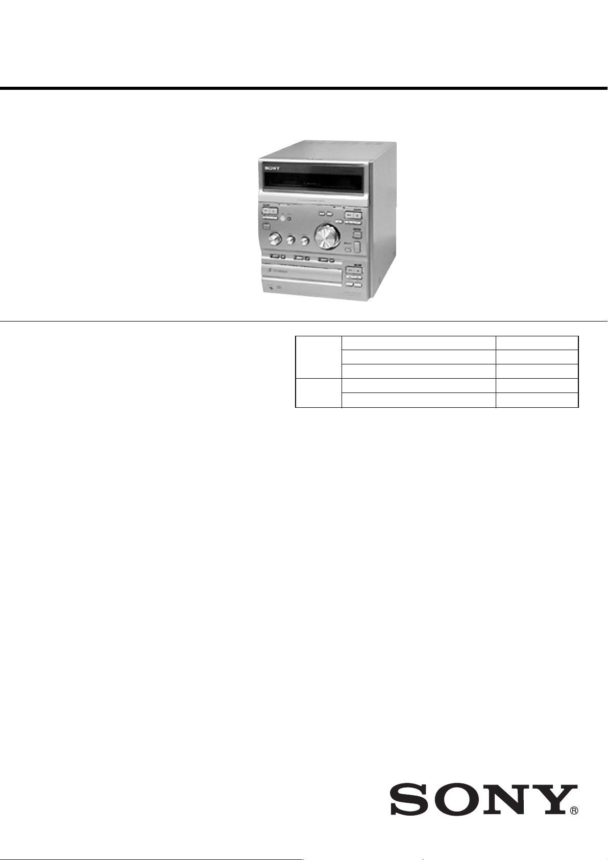
Sony HCD-CP333 User manual

HCD-CP333
US Model
Canadian Model
AEP Model
UK Model
E Model
SERVICE MANUAL
MICRO HI-FI COMPONENT SYSTEM
— Continued on next page —
SPECIFICATIONS
Ver 1.1 2003. 11
• HCD-CP333 is the Amplifier, CD player,
Tape Deck and Tuner section in
CMT-CP333.
Sony Corporation
Home Audio Company
Published by Sony Engineering Corporation
9-877-051-02
2003K16-1
© 2003.11
Amplifier section
For the U.S. model
AUDIO POWER SPECIFICATIONS
POWER OUTPUT AND TOTAL
HARMONIC DISTORTION:
With 6-ohm loads, both channels driven, from
120 - 10,000 Hz; rated 40 watts per channel
minimum RMS power, with no more than 10%
total harmonic distortion from 250 milliwatts to
rated output.
North American model
Continuous RMS power output (reference):
40 + 40 W
(6 ohms at 1 kHz, 10%
THD)
Total harmonic distortion less than 0.07% (6 ohms at
1 kHz, 32 W)
European model
DIN power output (rated): 32 + 32 W
(6 ohms at 1 kHz, DIN)
Continuous RMS power output (reference):
40 + 40 W
(6 ohms at 1 kHz, 10%
THD)
Music power output (reference):
100 + 100 W
Other models
The following measured at 230 V AC, 60 Hz
DIN power output (rated): 30 + 30 W
(6 ohms at 1 kHz, DIN)
Laser Semiconductor laser
(λ= 780 nm)
Emission
duration: continuous
Wavelength 780 - 790 nm
Frequency response 20 Hz - 20 kHz (±0.5 dB)
Tape player section
Recording system 4-track 2-channel stereo
Frequency response 50 - 13,000 Hz (±3 dB),
using a Sony TYPE I
cassette
Tuner section
FM stereo, FM/AM superheterodyne tuner
FM tuner section
Tuning range
North American model: 87.5 - 108.0 MHz
(100-kHz step)
Other models: 87.5 - 108.0 MHz
(50-kHz step)
Antenna FM wire antenna
Antenna terminals 75 ohm unbalanced
Intermediate frequency 10.7 MHz
Continuous RMS power output (reference):
38 + 38 W
(6 ohms at 1 kHz, 10%
THD)
The following measured at 220 V AC, 60 Hz
DIN power output (rated): 27 + 27 W
(6 ohms at 1 kHz, DIN)
Continuous RMS power output (reference):
35 + 35 W
(6 ohms at 1 kHz, 10%
THD)
Inputs
AUDIO IN MD (VIDEO) (phono jacks):
Sensitivity 500/250 mV,
impedance 47 kilohms
Outputs
CD DIGITAL OUT OPTICAL:
Optical
PHONES: Accepts headphones with
an impedance of 8 ohms
or more
SPEAKER: 6 ohms
CD player section
System Compact disc and digital
audio system
Model Name Using Similar Mechanism HCD-CP300
CD Mechanism Type CDM63K-K6BD44
Optical Pick-up Type KSM-213D
Model Name Using Similar Mechanism HCD-CP300
Tape Transport Mechanism Type CMBL6Z511A
CD
Section
Tape deck
Section

2
HCD-CP333
TABLE OF CONTENTS
General
Power requirements
North American model: 120 V AC, 60 Hz
European model: 230 V AC, 50/60 Hz
Other models: 110 - 120 V or 220 -
240 V AC , 50/60 Hz
Adjustable with voltage
selector
Power consumption
European model 70 W
0.4 W (at the power
saving mode)
Other models: 70 W
Dimensions (w/h/d) Approx. 225 ×273 ×
385 mm incl. projecting
parts and controls
Mass Approx. 7.3 kg
AM tuner section
Tuning range
North American model: 530 - 1,710 kHz
(with the tuning interval
set at 10 kHz)
531 - 1,710 kHz
(with the tuning interval
set at 9 kHz)
European model: 531 - 1,602 kHz
(with the tuning interval
set at 9 kHz)
Other models: 530 - 1,710 kHz
(with the tuning interval
set at 10 kHz)
531 - 1,602 kHz
(with the tuning interval
set at 9 kHz)
Antenna AM loop antenna, external
antenna terminal
Intermediate frequency 450 kHz
•Design and specifications are subject to change without notice.
1. SERVICING NOTES························································· 4
2. GENERAL············································································ 5
3. DISASSEMBLY·································································· 7
3-1. Cover (Upper) ································································· 8
3-2. Front Panel Section························································· 8
3-3. Tape Mechanism Deck-1 ················································ 9
3-4. Tape Mechanism Deck-2 ················································ 9
3-5. LED Board, CONTROL Board ···································· 10
3-6. Back Panel SubAssy, JACK Board ······························ 10
3-7. MAIN Board ································································· 11
3-8. POWER Board······························································ 11
3-9. CD Mechanism Deck (CDM63K-K6BD44) ················ 12
3-10.CD Board ······································································ 12
3-11.Base Unit (BU-K6BD44) ············································· 13
3-12.Tray Assy ······································································ 13
3-13.Silder (Loading)···························································· 14
3-14.TRAY SENSOR Board, MOTOR Board······················ 14
3-15.IN OUT SW Board ······················································· 15
3-16.Stocker Assy ································································· 15
3-17.CD Base Unit Assy, DISC SENSOR Board ················· 16
4.TEST MODE······································································ 17
5. ELECTRICAL ADJUSTMENTS································· 18
6. DIAGRAMS ······································································· 20
6-1. Note For Printed Wiring BoardsAnd Schematic
Diagrams······································································· 20
6-2. Block Diagrams ···························································· 21
6-3. Circuit Boards Location················································ 23
6-4. Printed Wiring Board – CD Board – ··························· 24
6-5. Schematic Diagram - CD Board -································· 25
6-6. Printed Wiring Board – TC Board – ····························· 26
6-7. Schematic Diagram – TC Board –································ 27
6-8. Printed Wiring Board – MAIN Board – ······················· 28
6-9. Schematic Diagram – MAIN Board (1/3) – ················· 29
6-10.Schematic Diagram – MAIN Board (2/3) – ················· 30
6-11.Schematic Diagram – MAIN Board (3/3) – ················· 31
6-12.Printed Wiring Board – CONTROL Section – ············· 32
6-13.Schematic Diagram – CONTROL Section – ················ 33
6-14.Printed Wiring Board – DRIVER Section – ················· 34
6-15.Schematic Diagram – DRIVER Section –···················· 35
6-16.Printed Wiring Board – POWER Board – ···················· 36
6-17.Schematic Diagram – POWER Board – ······················· 37
6-18.Printed Wiring Board – LCD Section – ························ 38
6-19.Schematic Diagram – LCD Section –··························· 38
6-20.IC Pin Function Description ·········································39
6-21.IC Block Diagrams ······················································· 41
7. EXPLODEDVIEWS························································ 44
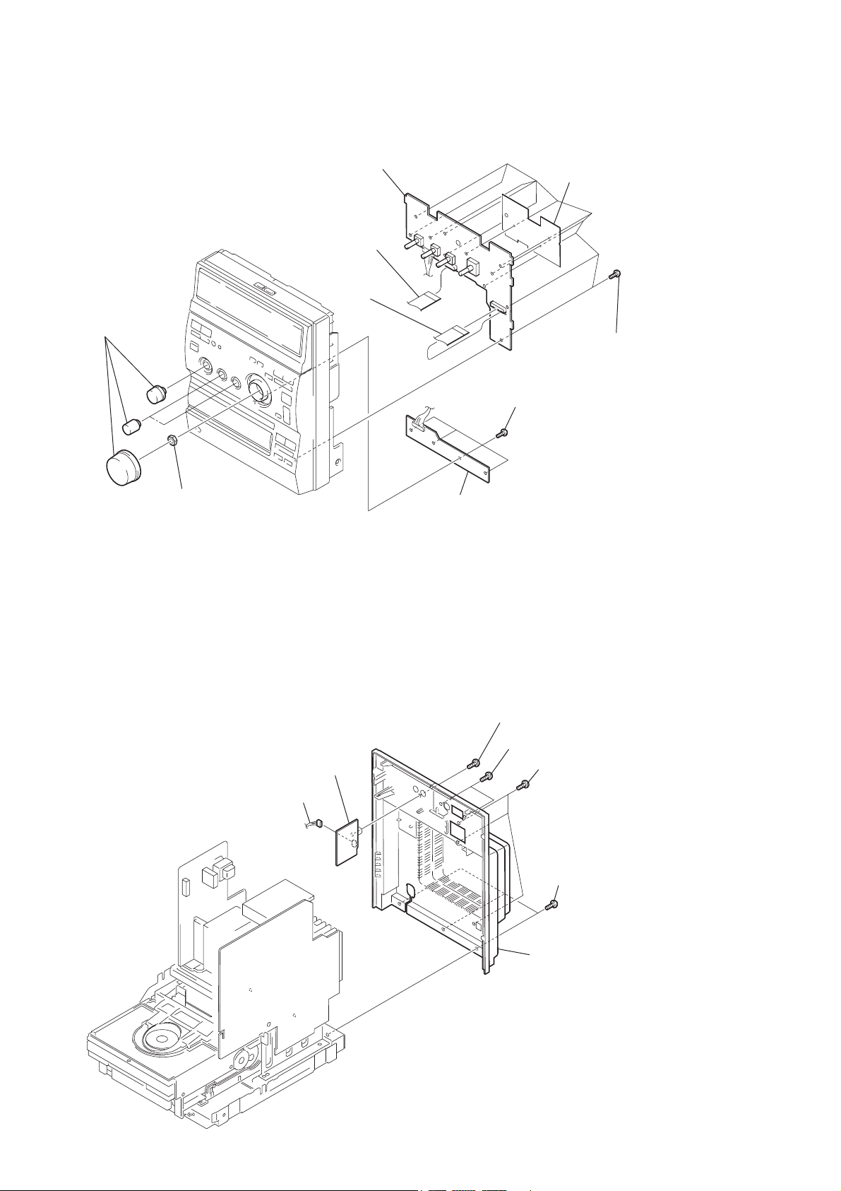
7-1. Cover Section································································ 44
7-2. Front Panel Section······················································· 45
7-3. Chassis Section ····························································· 46
7-4. CD Mechanism Deck-1 ················································ 47
7-5. CD Mechanism Deck-2 ················································ 48
7-6. KSM-213D ··································································· 49
8. ELECTRICAL PARTS LIST········································· 50
Ver 1.1 2003.11

3
HCD-CP333
SAFETY-RELATED COMPONENT WARNING!!
COMPONENTS IDENTIFIED BY MARK 0OR DOTTED LINEWITH
MARK 0ON THE SCHEMATIC DIAGRAMS AND IN THE PARTS
LIST ARE CRITICAL TO SAFE OPERATION. REPLACE THESE
COMPONENTS WITH SONY PARTS WHOSE PART NUMBERS
APPEAR AS SHOWN IN THIS MANUAL OR IN SUPPLEMENTS
PUBLISHED BY SONY.
ATTENTION AU COMPOSANT AYANT RAPPORT
À LA SÉCURITÉ!
LES COMPOSANTS IDENTIFÉS PAR UNE MARQUE 0SUR LES
DIAGRAMMES SCHÉMATIQUES ET LA LISTE DES PIÈCES SONT
CRITIQUES POUR LA SÉCURITÉ DE FONCTIONNEMENT. NE
REMPLACER CES COMPOSANTS QUE PAR DES PIÈSES SONY
DONT LES NUMÉROS SONT DONNÉS DANS CE MANUEL OU
DANS LES SUPPÉMENTS PUBLIÉS PAR SONY.
CAUTION
Use of controls or adjustments or performance of procedures
other than those specified herein may result in hazardous
radiation exposure.
This appliance is classified as a CLASS 1 LASER product.
The CLASS 1 LASER PRODUCT MARKING is located on
the rear exterior.
Laser component in this product is capable of emitting radiation
exceeding the limit for Class 1.
Notes on chip component replacement
•Never reuse a disconnected chip component.
•Notice that the minus side of a tantalum capacitor may be dam-
aged by heat.
Flexible Circuit Board Repairing
•Keep the temperature of the soldering iron around 270 ˚C dur-
ing repairing.
•Do not touch the soldering iron on the same conductor of the
circuit board (within 3 times).
•Be careful not to apply force on the conductor when soldering
or unsoldering.
SAFETY CHECK-OUT
After correcting the original service problem, perform the following
safety check before releasing the set to the customer:
Check the antenna terminals, metal trim, “metallized” knobs, screws,
and all other exposed metal parts for AC leakage.
Check leakage as described below.
LEAKAGE TEST
The AC leakage from any exposed metal part to earth ground and
from all exposed metal parts to any exposed metal part having a
return to chassis, must not exceed 0.5 mA (500 microamperes.).
Leakage current can be measured by any one of three methods.
1. A commercial leakage tester, such as the Simpson 229 or RCA
WT-540A. Follow the manufacturers’ instructions to use these
instruments.
2. A battery-operated AC milliammeter. The Data Precision 245
digital multimeter is suitable for this job.
3. Measuringthevoltagedrop across aresistorby means of aVOM
or battery-operatedAC voltmeter. The “limit” indication is 0.75
V, so analog meters must have an accurate low-voltage scale.
The Simpson 250 and Sanwa SH-63Trd are examples of a
passiveVOM that is suitable. Nearly all battery operated digital
multimeters that have a 2VAC range are suitable. (See Fig.A)
Fig. A. Using an AC voltmeter to check AC leakage.
1.5 k
Ω
0.15
µ
FAC
voltmeter
(0.75 V)
To Exposed Metal
Parts on Set
Earth Ground

4
HCD-CP333
The laser diode in the optical pick-up block may suffer electrostatic
break-down because of the potential difference generated by the
charged electrostatic load, etc. on clothing and the human body.
During repair, pay attention to electrostatic break-down and also
use the procedure in the printed matter which is included in the
repair parts.
The flexible board is easily damaged and should be handled with
care.
NOTES ON LASER DIODE EMISSION CHECK
The laser beam on this model is concentrated so as to be focused on
the disc reflective surface by the objective lens in the optical pick-
up block. Therefore, when checking the laser diode emission,
observe from more than 30 cm away from the objective lens.
NOTES ON HANDLING THE OPTICAL PICK-UP
BLOCK OR BASE UNIT
SERVICE POSTION
In checking the CD block, prepare jig (extension cable J-2501-011-
B).
SECTION 1
SERVICING NOTES
Connect jig (extension cable J-2501-011-B)
to the MAIN board (CN304) and CD board (CN101).
MAIN board
CD board
MODEL IDENTIFICATION
— BACK PANEL —
Parts No.
Power Voltage Indication
VOLTAGE SELECTOR
Switch
MODEL PARTS No.
AEP model 4-233-470-3s
UK model 4-233-470-3s
US model 4-233-470-4s
Canadian model 4-233-470-4s
E model 4-233-470-5sAC:110-120/220-240V
50/60Hz 70W
POWER VOLTAGE INDICATION
AC:230V 50/60Hz 70W
AC:120V 60Hz 70W

5
HCD-CP333
SECTION 2
GENERAL
1 DISC indicator wa
BASS ea
CD 1 wd
CD 1 Zwf
CD 2 wg
CD 2 Zwh
CD 3 wj
CD 3 Zwk
CD SYNC 7
CD uws
CD xqj
CD ./>qk
CD m/Mqk
DECK A EJECT Z5
DECK B EJECT Z6
DSG 4
FUNCTION es
PHONES jack wl
PLAY MODE w;
Remote sensor 3
REPEAT ql
TAPE A N1
TAPE B Y0
TAPE A x2
TAPE B xqa
TAPE A m/Mef
TAPE B m/Mqs
TAPE REC z8
TAPE X9
TREBLE e;
TUNER BAND qd
TUNING MODE qf
TUNING +/– qg
VOLUME qh
BUTTON DESCRIPTIONS
@/1 (power) ed
1234 5~6987q;
qa
qs
qd
qf
qg
qh
qj
qk
wl
e;
ed
es
ea
ef
wd~wk ws w;wa ql
Y
?/1
xMx
mMmM
X
z
ZZ
ux
.>
mM
ZZZ
Main unit
This section is extracted
from instruction manual.

6
HCD-CP333
Setting the time
1Turn on the system.
2Press TIMER SET on the remote.
If you are setting the clock for the first time,
go to step 5.
3Press ./>on the remote
repeatedly until “CLOCK” appears in
the display.
4Press ENTER on the remote.
The hour indication flashes.
5Press ./>on the remote
repeatedly to set the hour.
6Press ENTER on the remote.
The minute indication flashes.
7Press ./>on the remote
repeatedly to set the minute.
8Press ENTER on the remote.
The clock will begin operating.
To reset the system clock
Start over from step 1.
BASS/TREBLE ql
CD wj
DIRECTION qj
DISC1 wf
DISC2 wg
DISC3 wh
DISPLAY qs
DSG qa
ENTER qh
FUNCTION 5
MEMORY qk
PLAY MODE wl
SLEEP 1
STEREO/MONO qd
TAPE A/B wk
TIMER SELECT 2
TIMER SET 3
TUNER/BAND 7
TUNING MODE 6
VOL + qf
VOL – qg
BUTTON DESCRIPTIONS
Nwd
X8
x9
.ws
>0
mw;
Mwa
@/1 (power) 4
NX x
?/1
1234
6
5
wl
ql
w;~wa
ws
wd
qj
wk
wj 7
8
9
q;
qa
qd
qgqfqh
qs
wf~wh
qk
Remote Control

7
HCD-CP333
SECTION 3
DISASSEMBLY
•The equipment can be removed using the following procedure.
TRAY ASSY
STOCKER ASSY CD BASE UNIT ASSY,
DISC SENSOR BOARD
SLIDER (LOADING)
TRAY SENSOR BOARD, MOTOR BOARD
IN OUT SW BOARD
BASE UNIT (BU-K6BD44)
CD MECHANISM DECK (CDM63K-K6BD44)
FRONT PANEL SECTION
COVER (UPPER)
TAPE MECHANISM DECK-1 TAPE MECHANISM DECK-2
LED BOARD, CONTROL BOARD
BACK PANEL SUB ASSY, JACK BOARD MAIN BOARD
POWER BOARD
CD BOARD
SET
In order to remove stocker assy,
please remove tray assy, slider (loading) and tray sensor board.
Ver 1.1 2003.11

8
HCD-CP333
3-2. Front Panel Section
3-1. Cover (Upper) 1s
ix screws (+BTP 3
×
8)
4cover (upper)
2two case
screw
s
3two case
screws
qa s
crew (+KTP 3
×
6)
qs s
crew (+KTP 3
×
6)
qd
front panel section
q; t
wo screws (+BTP 3
×
8)
2c
onnector 2p (CN810)
3w
ire (flat type) 11p (CN303)
5w
ire (flat type) 21p (CN803)
6w
ire (flat type) 17p (CN801)
8w
ire (flat type) 17p (CN806)
7w
ire (flat type) 15p (CN805)
4w
ire (flat type) 11p (CN302)
1c
onnector 2p (CN809)
9c
onnector 4p (CN307)
Note : Follow the disassembly procedure in the numerical order given.

9
HCD-CP333
3-3. Tape Mechanism Deck-1
3-4. Tape Mechanism Deck-2
1two
screws (+BVTP 3
×
8)
3
4
5
2t
hree screws (+BVTP 3
×
8
)
6t
ape machanism deck
1c
assette holder (B) sub assy
3c
assette holder (A)
sub assy
2s
pring (casstte B)
7w
ire (flat type) 11p
(CN401)
qs b
racket (MD)
q;
TC board
qd w
ire (flat type) 11p
4s
pring (cassette A)
5s
crew (+BTP 3
×
8)
8t
wo screws (+BVTP tapping)
qa t
hree screws (+BVTP tapping)
qf t
wo screws (+BVTTWH tapping)
qg t
wo dampers
qh t
ape machanism dec
k
6s
hield case (TC)
9
Remove solderings.

10
HCD-CP333
3-6. Back Panel Sub Assy, JACK Board
3-5. LED Board, CONTROL Board
1
four knobs
2
hexagon nut
3
four
screws (IT3B 2.6
×
8)
5
eleven
screws (IT3B 2.6
×
8
)
6
shield sheet
4
LED board
9
CONTROL board
7
w
ire (flat type)
15p (CN807)
8
w
ire (flat type)
17p (CN808)
2t
hree screws (+BTP 3
×
8
)
3t
hree screws (+BTP 3
×
8)
4t
wo screws (+BTP 3
×
8)
5s
crew (+BTP 3
×
8)
6JACK
board
1c
onnector 3p (CN305)
7b
ack panel assy

11
HCD-CP333
3-7. MAIN Board
3-8. POWER Board
4s
crew (+BVTP 3
×
8)
6
MAIN board
5s
crew (+BVTP 3
×
12)
1c
onnector 9p (CN902)
2c
onnector 12p (CN313)
3w
ire (flat type) 21p (CN304)
4four
screws (+BVTP 4
×
8)
5
POWER board
2c
onnector 9p (CN902)
3c
onnector 2p (CN901)
1
earth plate

12
HCD-CP333
9f
our screws (+BTP 3
×
8)
3two
screws
(+BVTP 3
×
8)
8
cover (changer), MAIN board
q;
CD machanism deck (CDM63K-K6BD44)
5t
wo screws (+BVTP 3
×
8
)
4b
racket (retainer)
2s
crew (+BVTP 3
×
8)
1t
wo screws (+KTP 3
×
8)
7c
onnector 12p (CN701)
6w
ire (flat type)
21p (CN304)
HARNESS PROCESSING
4
w
ire (flat type) 21p (CN101)
3
w
ire (parallel) 16p (CN102)
2
Remove solder (four portions ).
1
screw
(+BTP 2.6
×
6)
5
CD board
3-9. CD Mechanism Deck (CDM63K-K6BD44)
3-10. CD Board

13
HCD-CP333
3three bosses
5
tray assy
3three bosses
2t
wo screws (+BTTP M2.6)
4
rack (center)
1t
wo screws (+BTTP M2.6)
5t
wo screws (IT3B 2.6
×
8)
2t
wo screws (+PTPWH 2.6
×
6
)
1s
crew, froating
7two
coil springs (insulator)
3c
oil spring (insulator)
3c
oil spring (insulator)
8two i
nsulators
4i
nsulator
4i
nsulator
6two stoppers (BU)
9b
ase unit
3-11. Base Unit (BU-K6BD44)
3-12. Tray Assy

14
HCD-CP333
3t
wo screws
(+BTTP M2.6)
1t
wo screws (+BTTP M2.6)
6t
wo screws (+PTPWH M2.6)
8
slider (loading)
7t
wo gears (slider)
4b
racket (retainer)
2b
racket (retainer)
2t
wo screws (+BTTP M2.6)
8t
wo screws (+BTTP M2.6)
4t
wo screws (+BTTP M2.6)
q; m
otor board
5TRAY SENSOR
board
9p
ulley (motor)
3h
older (sensor)
7b
elt
1c
onnector 5p (CN703)
6c
onnector 2p (CN702)
3-13. Silder (Loading)
3-14. TRAY SENSOR Board, MOTOR Board

15
HCD-CP333
2
t
wo screws (+BTTP M2.6)
1
Rotate the cam,
and up the stocker assy at the full.
stocker assy
3
c
onnector 2p (CN704)
4
IN OUT SW board
4
Slide the slider (BU.L),
slider (BU.R) in the direction of
arrow
A
at the full.
1s
crew (+BTTP M2.6)
2s
crew (+BTTP M2.6)
5st
ocker assy
A
A
3
Rotate the cam,
and up the stocker assy at the full.
3-15. IN OUT SW Board
3-16. Stocker Assy

17
HCD-CP333
[CD Ship Mode]
•This mode moves the optical pick-up to the position durable to
vibration. Use this mode when returning the set to the customer
after repair.
Procedure:
1. Press the ?/1button to turn the set ON.
2. Press three buttons x(TAPE A), x(CD), and Z(CD1)
simultaneously.
3. After the “STANDBY” display blinks six times, a message
“LOCK” is displayed on the liquid crystal display, and the CD
ship mode is set.
[GCTest Mode]
•This mode is used to check the software version, liquid crystal
display and keyboard.
Procedure:
1. Press three buttons x(TAPE A), x(CD) and ?/1 simul-
taneously.
2. Segments of the liquid crystal display are all turned on.
3. When you want to enter the software version display mode,
press the CD 1 button . The model number and destination are
displayed.
4. Each time the CD 1 button is pressed, the display changes
starting from MC version, GC version, CD version, CDD
version, CDMA version, CDMB version, BDA version, BDB
version , ST version, TA version, TM version, TC version and
MD version in this order.
5. Press the CD 2 button, and the key check mode is activated.
6. In the key check mode, “K 0J 0 V 0” is displayed. Each time
a button is pressed, “K 0” value increases. However, once a
button is pressed, it is no longer taken into account.
“V 0” value increases like 1, 2, 3 ... if rotating the VOLUME
knob clockwise, or it decreases like 0, 9, 8 ... if rotating
counterclockwise.
“J0” value increases if rotating the FUNCTION , BASS or
TREBLE knob clockwise, or it decreases if rotating
counterclockwise.
7. To exit from this mode, press three buttons in the same manner
as step 1, or disconnect the power cord.
SECTION 4
TEST MODE
[CD Ship (Memory Clear) Mode]
•Set the CD ship mode and set the default setup when shipped
from the factory at the nextAC power on.
Procedure:
1. Press the ?/1button to turn the set ON.
2. Select the function “CD ”.
3. Press three buttons x(TAPE A), x(CD), and Z(CD1)
simultaneously.
4. After the “STANDBY” display blinks six times, a message
“LOCK” is displayed on the liquid crystal display, and the CD
ship mode is set.

18
HCD-CP333 SECTION 5
ELECTRICAL ADJUSTMENTS
2. Turn the adjustment screw and check output peaks. If the peaks
do not match for L-CH and R-CH, turn the adjustment screw
so that outputs match within 1dB of peak.
0 dB=0.775 V
DECK SECTION
Note: Confirm each contents of this section first of all. If the results are
not satisfied, do the adjustment.
1. Demagnetize the record/playback head with a head
demagnetizer.
2. Do not use a magnetized screwdriver for the adjustments.
3. After the adjustments, apply suitable locking compound to the
parts adjust.
4. The adjustments should be performed with the rated power
supply voltage unless otherwise noted.
5. The adjustments should be performed in the order given in this
service manual. (As a general rule, playback circuit adjustment
should be completed before performing recording circuit
adjustment.)
6. The adjustments should be performed for both L-CH and R-
CH.
7. Switches and controls should be set as follows unless otherwise
specified.
•Test Tape
Record/Playback Head Azimuth Adjustment
Procedure:
1. Mode: Playback
set
MAIN board
SPEAKER terminals (SJ301
)
L-CH, R-CH
+
–
level meter
test tape
P-4-A63J
(10 kHz, –10 dB)
Screw
position
L-CH
peak
within
1 dB
Output
level
L-CH
peak R-CH
peak
within
1 dB
Screw
position
R-CH
peak
set
test tape
P-4-A63J
(10 kHz, –10 dB)
R-CH
oscilloscope
L-CH
R-CH
VH
waveform of oscilloscope
in phase 45
°
90
°
135
°
180
°
good wrong
MAIN board
SPEAKER terminals (SJ301
)
L-CH
Tape Signal Used for
P-4-A63J 10 kHz, –10 dB Azimuth Adjustment
3. Mode: Playback
4. Repeat step 1 to 3 in playback (REV) mode.
5. After the adjustments, apply suitable locking compound to the
pats adjusted.

19
HCD-CP333
CD SECTION
Note:
1. CD Block is basically constructed to operate without
adjustment.
2. UseYEDS-18 disc (3-702-101-01) unless otherwise indicated.
3. Use an oscilloscope with more than 10 MΩimpedance.
4. Clean the object lens by an applicator with neutral detergent
when the signal level is low than specified value with the
following checks.
5. Check the focus bias check when optical block is replaced.
Focus Bias Check
Procedure :
1. Connectoscilloscope toTP (RF) and TP (VC)onthe CD board.
2. Press the ?/1 button to turn the power on, and press the Z
(CD) button to open the CD disc tray.
3. Put disc (YEDS-18) in and press the u(CD) button to play-
back.
4. Confirm that oscilloscope waveform is as shown in the figure
below. (eye pattern)
A good eye pattern means that the diamond shape ( ) in the
center of the waveform can be clearly distinguished.
+
–
BD board
TP (RF)
TP (VC)
oscilloscope
(DC range)
VOLT/DIV: 200 m
V
TIME/DIV: 500 ns
level:
1.2
±
0.1 Vp-p
s
Checking Location:
– CD BOARD (Conductor Side) –
16
15
2
1
15
16 30
1
40
41
60 61
80
1
21 20
IC101
IC103
CN102
TP(RF)
TP(VC)

20
HCD-CP333 SECTION 6
DIAGRAMS
Note on PrintedWiring Boards:
•X: parts extracted from the component side.
•Y: parts extracted from the conductor side.
•W: indicates side identified with part number.
•: Pattern from the side which enables seeing.
•Indication of transistor.
Note on Schematic Diagram:
•All capacitors are in µF unless otherwise noted. pF: µµF
50 WV or less are not indicated except for electrolytics
and tantalums.
•All resistors are in Ωand 1/4W or less unless otherwise
specified.
•f: internal component.
•C: panel designation.
•A: B+ Line.
•B: B– Line.
•H: adjustment for repair.
•Voltagesare takenwithaVOM(Input impedance 10MΩ).
Voltage variations may be noted due to normal produc-
tion tolerances.
•Waveforms are taken with a oscilloscope.
Voltage variations may be noted due to normal produc-
tion tolerances.
•Circled numbers refer to waveforms.
•Signal path.
F: FM
E: PB (DECK A)
d: PB (DECK B)
G: REC (DECK B)
J: CD
c: DIGITAL OUT
f: MD
•Abbreviation
CND : Canadian model
E51 : Chilean and peruvian model
6-1. Note For Printed Wiring Boards And Schematic Diagrams
C
BThese are omitted.
E
Q
B
These are omitted.
CE
Q
B
These are omitted.
CE
Q
Caution:
Pattern face side: Partsonthe patternfaceside seenfrom
(Side A) the pattern face are indicated.
Parts face side: Parts on the parts face side seen from
(Side B) the parts face are indicated.
Note:
The components identified by
mark 0or dotted line with mark
0are critical for safety.
Replace only with part number
specified.
Note:
Les composants identifiés par
une marque 0sont critiques
pour la sécurité.
Ne les remplacer que par une
pièceportant lenumérospécifié.
Table of contents
Other Sony Stereo System manuals

Sony
Sony MHC-G101 Primary User manual

Sony
Sony SRS-XB3 User manual

Sony
Sony CAS-1 User manual

Sony
Sony CMT-GP6V User manual

Sony
Sony CMT-SPZ50 User manual

Sony
Sony MHC-WZ8D User manual

Sony
Sony MEX-BT3100P User manual

Sony
Sony XES-Z50 User manual

Sony
Sony HCD-V808 User manual

Sony
Sony MHC-GX9000 - Mini Stereo System User manual

Sony
Sony LBT-A790 User manual

Sony
Sony MHC-VX3 User manual

Sony
Sony MHC-EC59 User manual

Sony
Sony HCD-GNV99D User manual

Sony
Sony CMT-C7NT User manual

Sony
Sony MEX-N5000BT User manual

Sony
Sony MEX-BT4100E User manual

Sony
Sony MEX-BT2500 User manual

Sony
Sony AIWA XR-MN5 User manual

Sony
Sony game sync lbt-xg900av User manual