Sony HCD-H11 User manual

HCD-H11/H11J
SERVICE MANUAL
rHCD-H11 is the tuner deck, CD and
amplifier section in CHC-P11.
rHCD-H11J is the tuner deck, CD and
amplifier section in CHC-P11J.
Dolby noise reduction manufactured under license from
Dolby Laboratories Licensing Corporation.
“DOLBY” and the double-D symbol aare trademarks of
Dolby Laboratories Licensing Corporation.
CD player section
System Compact disc digital audio
system
Laser Semiconductor laser
(λ=780nm)
Emission duration :
continuous
Laser output Max 44.6µW*
*This output is the value measured at
a distance of 200 mm from the ob-
jective lens surface on the Optical
Pick-up Block with 7 mm aperture.
Wavelength 780–790 nm
Frequency response
2Hz – 20kHz
Signal-to-noise ratio
More than 65 dB
Dynamic rangeMore than 97 dB
Tuner section
FM stereo, FM/AM superheterodyne tuner
FM tuner section
Tuning range Except East European model :
87.5 - 108.0MHz (50kHz step)
SPECIFICATIONS
E2, Mexican, Argentine model :
AM : 531 - 1,710kHz (9kHz step)
AM : 530 - 1,710kHz (10kHz step)
Australian model
AM : 531 - 1,602kHz (9kHz step)
AM : 530 - 1,710kHz (10kHz step)
Antenna AM loop antenna
External antenna terminals
Intermediate frequency
450kHz
Tape player section
Recording system
4-track 2-channel stereo
Frequency response
(DOLBY NR OFF)
40 - 13,000 Hz (±3 dB),
using Sony TYPEI cassette
40 - 14,000 Hz (±3 dB),
using Sony TYPEII cassette
Wow and flutter
0.1% WRMS ±0.3%(DIN)
Amplifier section
Peak music power output
400W
–Continued on Page 2–
CD
Section
Model Name Using Similar Mechanism HCD-H801
CD Mechanism Type CDM28-5BD19
Base Unit Name BU-5BD19
Tape deck
Section Model Name Using Similar Mechanism HCD-H881
Tape Transport Mechanism Type TCM- 220WR2
MINI Hi-Fi COMPONENT SYSTEM
Photo : AEP Model
AEP Model
UK Model
E Model
Australian Model
HCD-H11
Saudi Arabia Model
HCD-H11/H11J
MICROFILM
East European model :
FM1 : 65 - 74 MHz (10kHz step)
FM2 : 87.5 - 108 MHz (50kHz
step)
Antenna FM lead antenna
Antenna terminals
75 ohm unbalanced
Intermediate frequency
10.7MHz
AM tuner section
Tuning range AEP, UK, East European, German
model :
MW : 531 - 1,602kHz
LW : 153 - 279kHz
Italian model :
MW : 522 - 1,611kHz
(9kHz step)
LW : 153 - 279kHz
E3, Saudi Arabia, Hong kong,
Malaysia, Singapore, Taiwan model :
MW : 531 - 1,602kHz
(9kHz step)
530 - 1,710kHz
(10kHz step)
SW : 5.95 - 17.9kHz

– 2 –
Continuous RMS power output
23W + 23W (4 ohms at
1kHz, 5% THD)
Inputs
MD IN : Sensitivity 450 mV,
impedance 47 kilohms
Outputs
MD OUT :Senitivity 250 mV, 1kΩ
PHONES (stereo phone jack) :
accept headphones of
8 ohms or more.
Supplied accessories
AM loop antenna (1)
Remote (1)
Sony SUM-3 (NS) batteries (2)
FM lead antenna (1)
General
Destination Power requirements Power
consumption
Mexican model 120v AC,60Hz
75W
AEP, UK, German,
Italian, East
European model 220 - 230V AC, 50/60Hz
Australian model 240V AC, 50/60Hz
E, Saudi Arabia,
Hong Kong,
Singapore, Argentine,
Malaysia, Taiwan
model
110 - 120V/ 220 - 240V
AC, 50/60Hz Adjustable
with the Voltage Selector
Dimensions Approx. 225 x 210x235 mm
(w/h/d) incl. projecting
parts and controls
Mass Approx.4.8kg
Design and specifications are subject to change without notice.
TABLE OF CONTENTS
Section Title Page
______ ____ ____
Specification ..................................................................................... 1
1. SERVICING NOTES ............................................................... 4
2. GENERAL
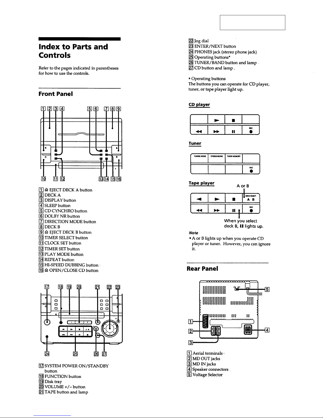
Index to Parts and Controls ........................................................ 3
3. DISASSEMBLY
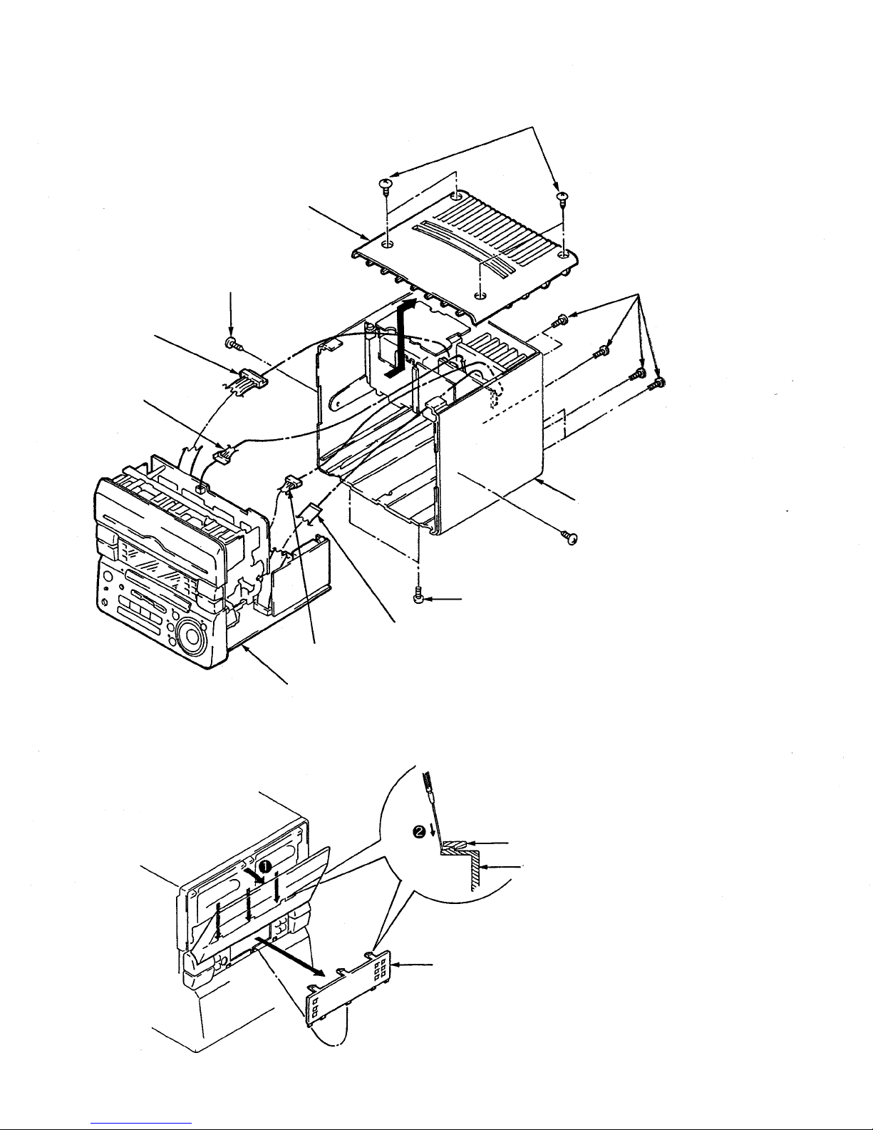
3-1. Front Panel Removal........................................................... 8
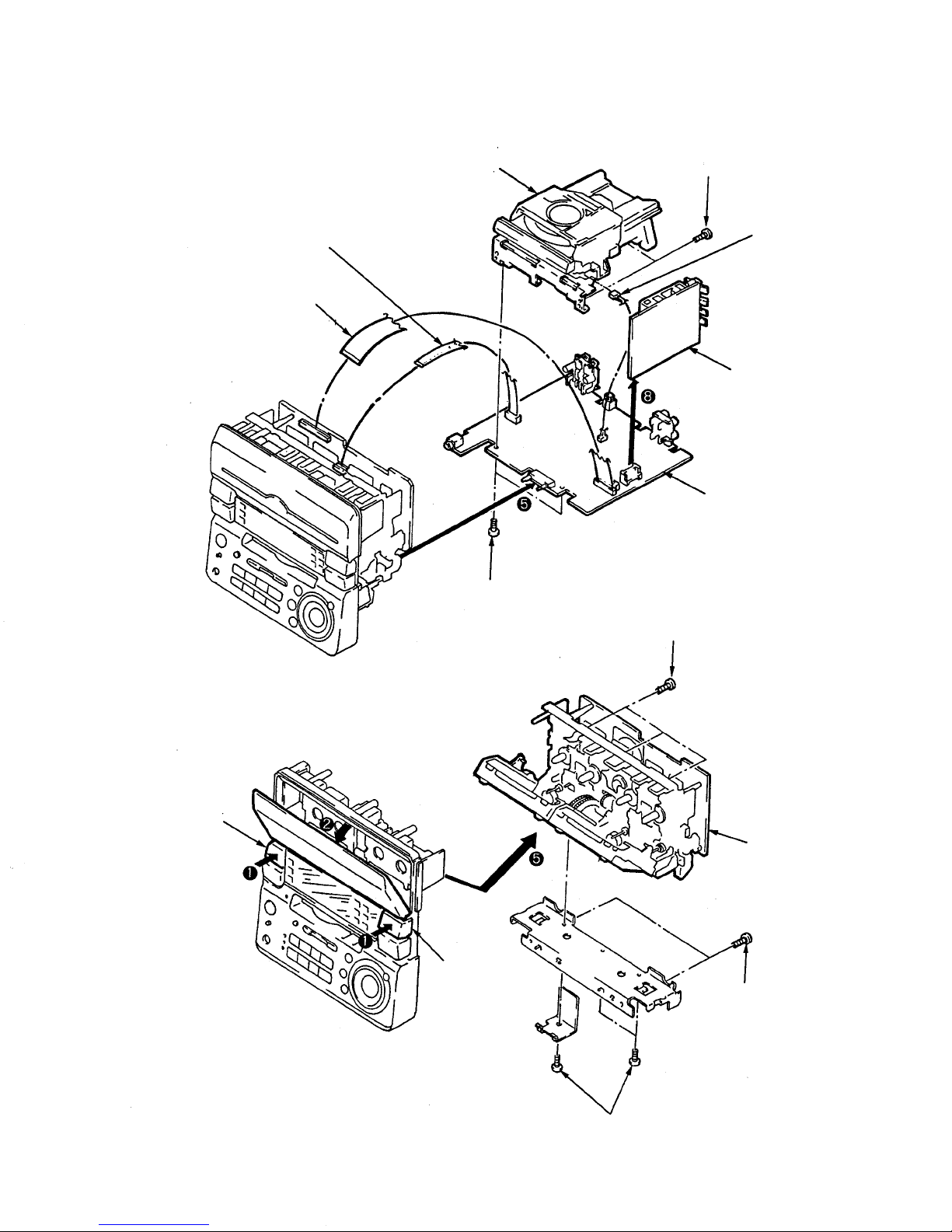
3-2. CD Mechanism, Main Board and TCB Board Removal .... 9
3-3. Mechanism Deck Removal ................................................. 9
4. ADJUSTMENTS
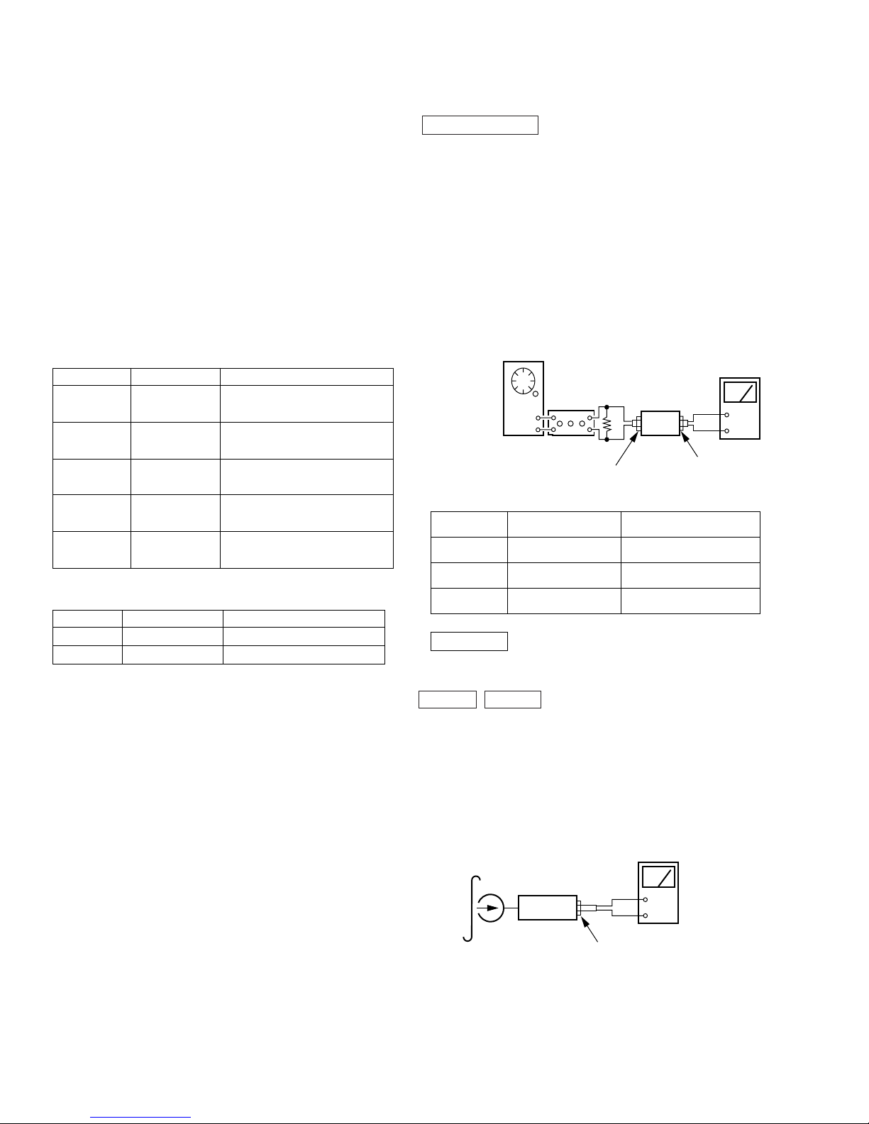
4-1. Mechanical Adjustment .................................................... 10
4-2. Electrical Adjustment........................................................ 10
5. EXPLANATION OF ICTERMINALS.................................. 17
6. DIAGRAMS
6-1. Block Diagram - CD Section ............................................ 21
6-2. Block Diagram - Main Section ......................................... 23
6-3. Circuit Board Location ..................................................... 27
6-4. Schematic Diagram - Main Section .................................. 28
6-5. Printed Wiring Boards - Main Section.............................. 33
6-6. Schematic Diagram - TCB Section................................... 36
(AEP,UK,G,IT,EE model)
6-7. Printed Wiring Boards - TCB Section .............................. 38
(AEP,UK,G,IT,EE model)
6-8. Printed Wiring Boards - TCB Section .............................. 39
(E3,EA,MY,SP,HK,TW,E2,MX,AR,AU model)
6-9. Schematic Diagram - TCB Section................................... 40
(E3,EA,MY,SP,HK,TW,E2,MX,AR,AU model)
6-10. Schematic Diagram - BD Section ................................... 45
6-11. Printed Wiring Boards - BD Section............................... 48
6-12. Printed Wiring Boards - Audio Section .......................... 49
6-13. Schematic Diagram -Audio Section............................... 50
6-14. Schematic Diagram - Panel Section................................ 54
6-15. Printed Wiring Boards - Panel Section ........................... 57
7. EXPLODED VIEWS
7-1. Chassis Section ................................................................. 59
7-2. Front Panel Section ........................................................... 61
7-3. TC Mechanism Section-1 ................................................. 63
7-4. TC Mechanism Section-2 ................................................. 64
7-5. CD Mechanism Section-1 ................................................. 65
7-6. CD Mechanism Section-2 ................................................. 66
8. ELECTRICAL PARTS LIST ................................................ 67

– 3 –
SECTION 1
SERVICING NOTES
NOTES ON HANDLINGTHE OPTICAL PICK-UP BLOCK
OR BASE UNIT
The laser diode in the optical pick-up block may suffer electrostatic
breakdown because of the potential difference generated by the
charged electrostatic load, etc. on clothing and the human body.
During repair, pay attention to electrostatic breakdown and also use
the procedure in the printed matter which is included in the repair
parts.
The flexible board is easily damaged and should be handled with
care.
NOTES ON LASER DIODE EMISSION CHECK
The laser beam on this model is concentrated so as to be focused on
the disc reflective surface by the objective lens in the optical pick-up
block. Therefore, when checking the laser diode emission, observe
more than 30 cm away from the objective lens.
CHUCK PLATE JIG ON REPAIRING
Onrepairing CDsection, playinga disc withouttheCD lid, useChuck
Plate Jig.
rCode number of Chuck Plate Jig : X-4918-255-1
MODEL IDENTIFICATION
(Specifcation Lable)
HCD-H11
HCD-H11J
MODEL NO.
COMPACT DISC DECK RECEIVER
AEP, UK, German, Italian,
East Europian model : AC220-230V⁄50/60Hz
Australian model : AC240V⁄50Hz
Maxican model : AC120V⁄60Hz
E, Saudi Arabia, Hong Kong,
Singapore, Argentine,
Malaysia, Taiwan model: AC110-120V/220-240V⁄50/60Hz
SAFETY-RELATED COMPONENT WARNING!!
COMPONENTS IDENTIFIED BY MARK !OR DOTTED LINE
WITH MARK !ONTHE SCHEMATIC DIAGRAMS AND INTHE
PARTS LIST ARE CRITICALTO SAFE OPERATION.
REPLACETHESE COMPONENTS WITH SONY PARTS WHOSE
PART NUMBERS APPEAR AS SHOWN IN THIS MANUAL OR IN
SUPPLEMENTS PUBLISHED BY SONY.
Laser component in this product is capable of emitting radiation
exceeding the limit for Class 1.
This appliance is classified as a
CLASS 1 LASER product. The
CLASS 1 LASER PRODUCT
MARKING is located on the
rear exterior.
CAUTION
Use of controls or adjustments or performance of procedures other
than those specified herein may result in hazardous radiation
exposure.
This caution label
islocated inside the
unit.

– 4 –
SECTION 2
GENERAL This section is extracted from
instruction manual.
(E, SaudiArabia, Argentine, Hong Kong,
Mexican, Malaysia, Singapore, Taiwan
model)

– 5 –

– 6 –
Notes for repairing CD MECHANISM section electric flow.
Two jigs (J-2501-091-A and J-2501-092-A) are necessary for the CD MECHANISM section electric flow.
Connect SET and JIG as shown in the figure below and turn the power switch on.
Jig
(J-2501-092-A)
CN101
(19 pin)
Jig
(J-2501-091-A)
CNU102
(19 pin)
CN291
(5 pin)

– 7 –
rDisc table getting out procedure on the power supply is OFF
Disc Table

– 8 –
SECTION 3
DISASSEMBLY
Note : Follow the disassembly procedure in the numerical order given.
3-1. FRONT PANEL REMOVAL
3
Screw (Case 3TP2)
2
Screw (Case 3TP2)
4
Plate, top
6
CN803
(8 pin)
7
CN602
(2 pin)
8
CN801
(3 pin)
Front Panel Section
9
Wire (Flat Type) (17 cove)
1
Screw (+BVTT3X6)
2
Screw (Case 3TP2)
Case
5
Screw (+BVTP3X10)
Front Panel
Window (DIS)
Window (DIS)
r
TO ADJUST THE AZIMUTH
1
Raise the cassette lid.
2
Press on the window (DIS) clips (3 locations)
with a tool such as a thin screwdriver and
remove the window (DIS).

– 9 –
3
Screw (+BVTP2.6X8)
4
CN291
(5 pin)
TCB Board
(TCB017)
6
Screw (+BVTT3X6)
Main Board
3
Screw (+BVTP2.6X8)
Mechanism Deck Section
(TCM-220WR2)
4
Screw (+BVTP2.6X8)
6
Screw (+BVTT3X6)
Button
(EJ-R)
Button
(EJ-L)
7
CD MECHANISM SECTION
(CDM28-5BD19)
2
Wire (Flat Type) (11 core)
1
Wire (Flat Type) (21 core)
3-2. CD MECHANISM, MAIN BOARD ANDTCB BOARD
3-3. MECHANISM DECK REMOVAL

– 10 –
4-2. ELECTRICAL ADJUSTMENTS
DECK SECTION
1. The adjustment should be performed in the publication.
(Be sure to make playback adjustment at first.)
2. The adjustment and measurement should be performed for
both L-CH and R-CH.
rSwitch position
DOLBY NR switch : OFF
TIMER switch : OFF
DIRECTION MODE switch : A
3. Deck section electrical adjustment are made in test mode by
pressing TUNER/BAND, DISPLAY, and FUNCTION at the
same time.
– Record Mode –
set
MD OUT
Level meter
+
–
MD IN
AF OSC
attenuator 600
Ω
rTestTape
Tape Contents Use
P-4-A 100 10 kHz, –10dB Head Azimuth Adjustment
P-4-L300 315Hz, 0dB Level Adjustment
WS-48B 3kHz, 0dB Tape Speed Adjustment
0dB=0.775V
Record/Playback Head Azimuth Adjustment
DECK A DECK B
rSetup for adjustment
When adjusting the azimuth remove, the Window (DIS) in the
center of the front panel. (Refer to page 8.)
Procedure :
1. Forward Playback mode
Reverse Playback mode
set
MD OUT
+
-
test tape
P-4-A100
(10kHz, – 10dB) Level mete
r
SECTION 4
ADJUSTMENTS
4-1. MECHANICAL ADJUSTMENTS
PRECAUTION
1. Clean the following parts with a denatured-alcohol-moistened
swab : record/playback head pinch roller
erase head rubber belts
capstan
2. Demagnetize the record/playback head with a head demagnetizer.
3. Do not use a magnetized screwdriver for the adjustments.
4. After the adjustments, apply suitable locking compound to the
parts adjusted.
5. The adjustments should be performed with the rated power sup-
ply voltage unless otherwise noted.
rTorque Measurement
Mode Torque Meter Meter Reading
Forward CQ-102C 36 to 61g•cm
(0.50 – 0.84 oz•inch)
Forward
Back Tension CQ-102C 2 to 6g•cm
(0.026 – 0.082 oz•inch)
Reverse CQ-102RC 36 to 61g•cm
(0.50 – 0.84 oz•inch)
Reverse
Back Tension CQ-102RC 2 to 6g•cm
(0.026 – 0.082 oz•inch)
FF, REW CQ-201B 61 to 143g•cm
(0.85 – 1.98 oz•inch)
rTapeTension Measurement
Mode Torque Meter Meter Reading
Forward CQ-403A more than 100g (3.53 oz)
Reverse CQ-403R more than 100g (3.53 oz)

– 11 –
Tape Speed Adjustment DECK A DECK B
Procedure :
rPerform high speed adjustment before normal speed adjustment.
Mode : Playback
+
–
MD OUT
set
frequency counter
test tape
WS-48B
(3kHz, – 0dB)
Speed Deck Adjustment Frequency counter
*High A RV652 5,970 to 6,030Hz
B RV652
Normal A RV651 2,940 to 3,090Hz
B RV651
*Continus to press HIGH SPEED DUBBING switch (S507) in
playback mode : High speed palyback.
Frequency difference between the begining and the end of the tape
should be within ± 3%.
Frequency difference between deck A and deck B the biginning
of the tape should be within 1.5%.
Adjustment Location : AUDIO board.
(see page 12)
Playback Level Adjustment DECK A DECK B
Procedure :
Mode : Playback
set
MD OUT
+
–
test tape
P-4-L300
(315kHz, –10dB) Level mete
r
Deck A is RV311 (L-CH) and RV411 (R-CH), deck B is RV301 (L-
CH) and RV401 (R-CH) so that adjustment within adjustment level
as follows.
Adjustment Level :
MD OUT level : – 3.5 ± 0.5dB (0.489 to 0.546V)
Level Difference between Channels : within 0.5dB
Confirm the OUT PUT level does not change in playback mode while
changing the mode from playback to stop several times.
Adjustment Location : AUDIO board.
(see page 12)
L-CH
peak R-CH
peak
L-CH
peak
R-CH
peak
Screw
position
output
level within
1 dB within
1 dB
screw angle
2. Turn the adjustment screw for the maximum output levels. If
these levels do not match,turn the adjustment screw until both
of output levels match together within 1dB.
3. Playback Mode
MD OUT
screen patten
VH
set
test tape
P-4-A100
(10kHz, – 10dB) Oscilloscope
R-CH
in phase 45˚ 90˚ 135˚ 180˚
good wrong
L-CH
4. Change the review playback mode and repeat the steps 1 to 3.
5. After the adjustment, lock the adjustment screw with suit
able locking compound.
Adjustment Location :
– record/playback head (Deck A and B)
Dack A Dack B
forward reverse
Adjustment Screw

– 12 –
Record Bias Adjustment DECK B
Procedure :
1. Record mode
set
AF OSC
attenuator 600
Ω
MD IN
1) 315 Hz
2) 10KHz 38.8mV (–26dB)
blank tape
CS-123
2. Playback mode
set
MD OUT
+
–
recorded
portion Level mete
r
3. Confirm playback the signal recorded in step 1 become
adjustment level as follows.
4. If these levels do not adjustment level, adjustment the RV341
(L-CH) and RV441 (R-CH) to repeat step 1 and 4.
Adjustment level :
Playback output of 315Hz to playback output of 10kHz : – 0.5dB to
0.5dB. (– 1.3 to 1.3mV)
Adjustment Location : AUDIO board .
Record Level Adjustment DECK B
Procedure :
1. Record mode
set
AF OSC
attenuator 600
MD IN
315Hz 38.8mV (–26dB)
blank tape
CS-123
Ω
2. Playback mode
set
MD OUT
+
–
recorded
portion Level mete
r
3. Confirm playback the signal recorded in step become
adjustment level as follows.
4. If these levels do not adjustment level, adjust the RV401 (L-CH)
and RV451 (R-CH) to repeat step 1 and 4.
Adjustment Level :
OUT PUT level : – 28dB ± 0.5dB (29.1 to 32.7mV)
Adjustment Location : MAIN board
Adjustment Location :
[ AUDIO BOARD ] – Component side –
RV341 : Record Bias (L-CH)
RV441 : Record Bias (R-CH)
RV301 : Playback Level (Deck B L-CH)
RV401 : Playback Level
(Deck B R-CH)
RV651 : Tape Speed (Normal)
RV652 : Tape Speed
(HIGH)
RV311 : Playback Level
(Deck A L-CH)
RV411 : Playback Level
(Deck A R-CH)
[ MAIN BOARD ] – Component side –
RV401 :
Record Level (L
)
RV451 :
Record Level (R)

– 13 –
TUNER SECTION
Precautions in Repairing
Note. 1 : The adjustment should be performed in the publication.
(MW nFM nSW)
Note. 2 : As a front-end (FE1) is difficult to repair if faulty, replace it
with new one.
rAbbreviation
AUS : Australian IT : Italian
G : German AR : Argentine
EA : Saudi Arabia HK : Hong Kong
MX : Mexican. SP : Singapore
MY : Malaysia TW : Taiwan
EE : East European
E2 : Tuner sections SW BAND do not exist.
E3 : Tuner sections SW BAND exist.
MWTuned Indication Lighting Level
Setting :
Band : MW
set
AM RF signal
generator
loop antenna A
loop antenna B
Carrier frequency : 999kHz (at
9kHz step) or
1,050kHz (at
10kHz step)
Modulation : 400Hz 30% modulation
Procedure :
1. Set loop antennaA so that the loop antenna B input level becomes
55dBµ/m (0.6mV/m)
2. Tune the set to 999kHz (at 9kHz step) or 1,050kHz (at 10kHz
step).
3. Adjust RV41 so that the TUNED indicatior goes on.
Adjustment Location : TCB board (see page 14)
FMTuned Indication Lighting Level
Note : Always make the tuning level adjustment first.
(Since it affects the FM tuning level.)
Setting :
Band : FW
FM RF stereo signal
generator
75
Ω
coaxial
FM ANTENNA terminal
set
Carrier frequency : 98MHz
Modulation : 1kHz, 75kHz (100%)
Output level : 0.018mV (25dB )
µ
Procedure :
1. Tune the set to 98MHz.
2. Adjust RV42 so that the TUNED indicator goes on.
Adjustment Location : TCB board (see page 14)
SW ControlVoltage Adjustment
(Frequency Coverge Adjustment)
(E3,EA,MY,SP,HK,TW model)
Setting :
Band : SW
Procedure :
1. Connect digital Voltmeter to diode D1 center lead and ground.
2. Adjust for a following value reading on digitalVoltmeter.
Set frequency Adjustment
part Reading on digital
voltmeter
SW 5.95MHz T2 1.2Vdc
17.9MHz CV2 8.5Vdc
Adjustment Location : TCB board (see page 14)
SWTracking Adjustment
(E3,EA,MY,SP,HK,TW model)
Setting :
Band : SW
+
–
AM RF signal
generator
AM ANTENNA terminal
SPEAKER terminal
Modulation : 400Hz
30% modulation
set
Level mete
r
Procedure :
Adjust for maximum reading on Level mater.
Set frequency Adjustment
part
SW 7MHz T1
17MHz CV1
rRepeat the procedures is each adjustment several times, and the
frequencycoverageand tracking adjustmentshouldbe finally done
by the trimmer capacitors.
Adjustment Location : TCB board (see page 14)

– 14 –
CD SECTION
Note :
1. CD Block basically constructed to operate without adjustment.
Therefore, check each item in order given.
2. UseYEDS-18 disc (3-702-101-01) unless otherwise indicated.
3. Use the oscilloscope with more than 10MΩimpedance.
4. Clean an object lens by an applicator with neutral detergent when
the signal level is low than specified value with the following
checks.
Focus Bias Adjustment
This adjustment is to be done when the optical block is replaced.
Adjustment procedure :
+
–
oscilloscope
(DC range)
TP (RF)
BD board
TP (VC)
1. Connect oscilloscope to test point TP (VC) and TP (RF) on BD
board.
2. Ground main board IC101 (pin(£) with the lead wire.
3. Turned power switch ON. (Stop mode)
4. Put disc (YEDS-18) in and press the (button.
5. Press the Pbutton. (Tracking servo ON)
6. Adjust RV101 so that the oscilloscope waveform is as shown in
the figure below (eye pattern).
A good eye pattern means that the diamond shape (◊) in the center
of the waveform can be clearly distinguished.
7. After adjustment, remove the lead wire connecd in step 2.
rRF signal reference waveform (eye pattern)
VOLT/DIV : 0.2V
TIME/DIV : 500n
s
1.3
±
0.3Vp-p
When observing the eye pattern, set the oscilloscope forAC range
and raise vertical sensitivity.
Adjustment Location : BD board. (see page 15)
S-Curve Check
+
–
oscilloscope
TP (FEO)
BD board
TP (VC)
Procedure :
1. Connect oscilloscope to test point TP (FEO) and BD board.
2. Connect between test point TP (FOK) and TP (GND) by lead wire.
3. Turned Power switch on.
Adjustment Location
[TCB BOARD]– Conductor side –
D1 FE1
T1 : SW Tracking Adjustment
RV42 :
FW Tuned indication
Lighting Level
RV41 :
MW Tuned indication
Lighting Level
CV1 : SW Tracking Adjustment
T2 :
SW Control Voltage
Adjustment
CV2 :
SW Control Voltage
Adjustment

– 15 –
4. Put disc (YEDS-18) in and turned Power switch on again and
actuate the focus search. (actuate the focus search when disc table
is moving in and out.)
5. Check the oscilloscope waveform (S-curve) is symmetrical
between A and B. And confirm peak to peak level within
2.4±0.7Vp-p.
S-curve waveform
symmetry
within 2.4
±
0.7Vp-p
A
B
6. After check, remove the lead wire connected in step 2.
Note : rTry to measure several times to make sure that the ratio of
A : B or B : A is more than 10 : 7.
rTake sweep time as long as possible and light up the brigh-
ness to obtain best waveform.
Adjustment Location : BD board. (see page 15)
RF Level Check
+
–
oscilloscope
TP (RF)
BD board
TP (VC)
Procedure :
1. Connect oscilloscope to test point TP (RF) on BD board.
2. Turned Power switch on.
3. Put disc (YEDS-18) in and press the (button.
4. Confirm that oscilloscope waveform is clear and check RF signal
level is correct or not.
Note :
Clear RF signal waveform meansthat the shape “ ◊” can be clearly
distinguished at the center of the waveform.
RF signal waveform
VOLT/DIV : 200mV
TIME/DIV : 500ns
level : 1.3
±
0.3Vp-p
Adjustment Location : BD board. (see page 15)
E-F Balance Check
+
–
oscilloscope
(DC range)
TP (TEO)
TP (VC)
BD board
Procedure :
1. Ground main board IC101 (pin (£) with the lead wire.
2. Connect oscilloscope to test point TP (TEO) on BD board.
3. Turned Power switch on.
4. Put disc (YEDS-18) in and press the (button.
5. Confirm that the osilloscope waveform is symmetrical on the
top and bottom in relation to 0V, and check this level.
Traverse waveform
specified value :
r
A–B
2 (A+B) X100 = less than ±7%
r
A+B = 300 ±100mVp-p
level : 300
±
100mVp-p
A
B
0V
6. Remove the lead wire connected in step 1.
Focus/Tracking Gain Adjustment (RV102, RV103)
This gain has a margin, so even if it is slightly off. There is no prob-
lem.
Therefore, do not perform, this adjustment.
Please note that it should be fixed to mechanical center position when
you moved and do not know original position.
Adjustment Location :
[BD BOARD]– Conductor side –
IC102 FEI
TEI
FOK
IC101
RF
RV101
RV102
IC104
FEO
TEO VC
PCK
GND
RV103

– 16 –
IC101TMP87CP64YF - 6335 (MASTER CONTROL)
SECTION 5
EXPLANATION OF ICTERMINALS
Pin No. Pin name I/O Description
1VSS – Ground
2 X OUT O Main system clock. (10MHz)
––––––––––––––––––––––––––––––––––––––––––––––––––––––––––––––––––––––––––––––––––––––––––––
3 X IN I
–––––––––––––––
4RESET I Reset signal input terminal.
5 X OUT O Sub system clock.(32kHz).
––––––––––––––––––––––––––––––––––––––––––––––––––––––––––––––––––––––––––––––––––––––––––––
6 X IN I
7 GND – Ground.
–––––––––––––––––––
8BACK UP I BACK-UP mode input terminal.
9 COUNT SW – Not used. (Ground)
10 INIT SW – Not used. (Ground)
11 DISC SENS – Not used. (Ground)
12 MID SENS – Not used. (Ground)
13 CD XRST O CD Reset output. “L” : RESET
14 POWER O Power on output. “L” : ON
15 MUTE O Mute output. “L” : MUTE
16 MPX – Not used. (Open)
17 KEYCON LATCH – Not used. (Open)
18 VOL LATCH O Latch output to volume control. (TC9210P)
19 ST MUTE – Not used. (Open)
20 ST FM – Not used. (Open)
21 FUNC A O
––––––––––––––––––––––––––––––––––––––––––––––––––––––––––––––––––––––––––––––––––––––––––––
22 FUNC B O Function Select.
––––––––––––––––––––––––––––––––––––––––––––––––––––––––––––––––––––––––––––––––––––––––––––
23 FUNC C O
24 GEQ.LATCH O Latch output to gray control. (M6243FP)
25 RDS. INT I Not used. (+5V)
26 SCOR (DSP) I Sub code sync SO+SI detection input from DSP. (CXD2507AQ)
27 CIN / SENS I SENS input from DSP. (CXD2507AQ)
28 CD POWER O Power on output. “H” : ON
29 CDG LATCH – Not used. (Open)
30 DBFB- 2 – Not used. (Open)
31 MUTE – Not used. (Open)
32 CE O Chip enable output to tuner PLL IC. (LC72130)
33 STEREO I FM/AM Stereo identification. “L” : STEREO
34 TUNED I FM/AM Tuning identification. “L” : TUNING
35 SQ-RDS-CLK O Sub-code Q data scanning clock output to DSP (CXD2507AQ), RDS clock output.
36 SQ-RDS-DI I Sub-code Q data input from DSP (CXD2507AQ), RDS data input.
37 RDS-RESET – Not used. (Open)
38 CLK O System clock output.
39 D. IN I Serial data input from tuner.
40 D. OUT O Serial data (COMN) output.
FUNCTION FUNC A FUNC B FUNC C
ST L L H
CD L H H
TC H L H
MDHH L

– 17 –
Pin No. Pin name I/O Description
41 CDG MUTE – Not used. (Open)
42 REQ GM I Data transmission request input from system control.
43 MREQ O Not used. (+5V)
44 CLK MG O Clock output for communications with system control.
45 D. GM I Serial data input from system control.
46 D. MG O Serial data output to system control.
47 RDY I/O System control Ready signal input / output. “L” : READY
48 VAREF – Power supply. (+5V)
49 VASS – Ground
50 VSS – Ground
51 VDD – Power supply. (+5V)
52 URGENT. SIG I Not used. (+5V)
53 URGENT. STBY I Not used. (Open)
–––
54 BUGY/N – Not used. (Ground Connected)
55 ADJUSTOR – Not used. (“H” LEVEL)
56 ADJUST2 – Not used. (“H” LEVEL)
57 MAGIC SPEED – Not used. (“H” LEVEL)
58 SPEC I Not used. (“H” LEVEL)
59 DIST I Model Select input . (A/D Converter)
60 SPEED – Not used. (“H” LEVEL)
61 BREAK – Not used. (“H” LEVEL)
62 B-PLAY I Deck-B PLAY Switch input. “H” : PLAY
63 B-SHUT I Deck-B Reel table signal input.
64 B-HALF I Deck-B Record prevention claw A, B detection input.
65 A-SHUT I Deck-A Reel table signal input.
66 A-PLAY I Deck-A PLAY Switch input. “H” : PLAY
67 A-HALF I Deck-A HALF SW input.
68 CAPM H/L O Capstan motor speed selector. “H” : Normal speed “L” : High speed
69 CAPM ON/OFF O Capstan motor ON/OFF. “L” : ON
70 TRIG H/L O
––––––––––––––––––––––––––––––––––––––––––––––––––––––––––––––––––––––––––––––––––––––––––––
71 B TRG O Trigger motor control output.
––––––––––––––––––––––––––––––––––––––––––––––––––––––––––––––––––––––––––––––––––––––––––––
72 A TRG O
73 RELAY O Control output to REC/PB select switch. (IC602)
74 A/B O Dolby IC PB input Deck A/B select output. “L” : A, “H” : B
75 NORM/HIGH O EQ Select switch output for normal / high speed. “H” : High speed
76 BIAS ON/OFF O BIAS Oscillation ON/OFF control. “H” : ON
77 RM ON/OFF O REC Mute output. “L” : MUTE
78 REC/PB O DOLBY IC REC/PLAY Select output. “H” : REC
79 NR O DOLBY ON/OFF Control output. “H” : ON
80 LM O LINE Mute output. “L” : MUTE
81 PASS O PASS Amplifier switch output to DOLBY IC. (IC401)
82 CMD2 – Not used. (Open)
83 UP MOTOR – Not used. (Open)
84 DOWN MOTOR – Not used. (Open)
85 TABLE R – Not used. (Open)

– 18 –
86 TABLE L – Not used. (Open)
87 LOAD OUT O Loading motor (M903) Load out output.
88 LOAD IN O Loading motor (M903) Load in output.
89 DF-LATCH O Latch output to digital filter. (PCM1701U)
90 XLT O Serial data latch output to DSP. (CDX2507AQ)
91 FOCUS SW O High-region gain down output to focus servo. (CXA1782BQ)
92 HIGH DUBB – Not used. (“H” LEVEL)
93 TEST 1 – Not used. (“H” LEVEL)
94 OUT SW I CD Tray output detection input.
95 IN SW I CD Tray input detection terminal.
96 UP SW – Not used. (Ground)
97 PANEL SW – Not used. (Ground)
98 CLOSE SW – Not used. (Ground)
99 OPEN SW – Not used. (Ground)
100 VDD – Power supply. (+5V)
Pin No. Pin name I/O Description

– 19 –
IC501 CXP82612-016Q (SYSTEM CONTROL DRIVE)
1 ENC I Volume encoder input terminal.
2 SIRCS I Remote commander signal input.
3 REQ. MG I Data transmission request input from master control.
4 REQ. GM O Data transmission request output to master control.
5 LED1 O LED DRIVE Output.
6 LED2 – Not used. (Open)
7 LED3 – Not used. (Open)
8 LED4 – Not used. (Open)
9 LED5 O PLAY, PAUSE LED Output.
10 RDY I/O Master control Ready signal input / output. “L” : Ready
11 SCK. IN I Clock output for communications with master control.
12 SD. IN I Serial data input from master control.
13 SD. OUT O Serial data output to master control.
14 LED-PAUSE O REC, PAUSE LED Output.
15 LED-CD O ROCK LED Output.
16 LED-TUNER/BAND O JAZZ, DRECTION MODE LED Output
17 LED-TAPE O CLASSIC, DANCE LED Output.
18 LED-FWD,STOP,FF&REW O TUNER LED Output.
19 LED-DECK A/B & REV O CD, TIMER LED Output.
20 LED-A O ENTER / NEXT, TUNER / BAND LED Output.
21 LED-B O A, B LED Output.
22 KEY1 I
––––––––––––––––––––––––––––––––––––––––––––––––––––––––––––––––––––––––––––––––––––––––––––
23 KEY2 I Key input. (A/D Converter)
––––––––––––––––––––––––––––––––––––––––––––––––––––––––––––––––––––––––––––––––––––––––––––
24 KEY3 I
––––––––––––––––––––––––––––––––––––––––––––––––––––––––––––––––––––––––––––––––––––––––––––
25 KEY4 I
26 PBF1 I
––––––––––––––––––––––––––––––––––––––––––––––––––––––––––––––––––––––––––––––––––––––––––––
27 PBF2 I Not used. (Ground)
––––––––––––––––––––––––––––––––––––––––––––––––––––––––––––––––––––––––––––––––––––––––––––
28 PBF3 I
––––––––––––––––––––––––––––––––––––––––––––––––––––––––––––––––––––––––––––––––––––––––––––
29 PBF4 I
––––
30 RST I Reset signal input terminal.
31 X IN I system clock. (4MHz)
––––––––––––––––––––––––––––––––––––––––––––––––––––––––––––––––––––––––––––––––––––––––––––
32 X OUT O
33 VSS – Gound
34 P29 O
––––––––––––––––––––––––––––––––––––––––––––––––––––––––––––––––––––––––––––––––––––––––––––
35 P28 O
––––––––––––––––––––––––––––––––––––––––––––––––––––––––––––––––––––––––––––––––––––––––––––
36 P27 O
––––––––––––––––––––––––––––––––––––––––––––––––––––––––––––––––––––––––––––––––––––––––––––
37 P26 O
––––––––––––––––––––––––––––––––––––––––––––––––––––––––––––––––––––––––––––––––––––––––––––
38 P25 O
––––––––––––––––––––––––––––––––––––––––––––––––––––––––––––––––––––––––––––––––––––––––––––
39 P24 O LED Drive.
––––––––––––––––––––––––––––––––––––––––––––––––––––––––––––––––––––––––––––––––––––––––––––
40 P23 O
––––––––––––––––––––––––––––––––––––––––––––––––––––––––––––––––––––––––––––––––––––––––––––
41 P22 O
––––––––––––––––––––––––––––––––––––––––––––––––––––––––––––––––––––––––––––––––––––––––––––
42 P21 O
––––––––––––––––––––––––––––––––––––––––––––––––––––––––––––––––––––––––––––––––––––––––––––
43 P20 O
––––––––––––––––––––––––––––––––––––––––––––––––––––––––––––––––––––––––––––––––––––––––––––
44 P19 O
Pin No. Pin name I/O Description

– 20 –
Pin No. Pin name I/O Description
45 P18 O
––––––––––––––––––––––––––––––––––––––––––––––––––––––––––––––––––––––––––––––––––––––––––––
46 P17 O
––––––––––––––––––––––––––––––––––––––––––––––––––––––––––––––––––––––––––––––––––––––––––––
47 P16 O
––––––––––––––––––––––––––––––––––––––––––––––––––––––––––––––––––––––––––––––––––––––––––––
48 P15 O
––––––––––––––––––––––––––––––––––––––––––––––––––––––––––––––––––––––––––––––––––––––––––––
49 P14 O
––––––––––––––––––––––––––––––––––––––––––––––––––––––––––––––––––––––––––––––––––––––––––––
50 P13 O
––––––––––––––––––––––––––––––––––––––––––––––––––––––––––––––––––––––––––––––––––––––––––––
51 P12 O
––––––––––––––––––––––––––––––––––––––––––––––––––––––––––––––––––––––––––––––––––––––––––––
52 P11 O
––––––––––––––––––––––––––––––––––––––––––––––––––––––––––––––––––––––––––––––––––––––––––––
53 P10 O
––––––––––––––––––––––––––––––––––––––––––––––––––––––––––––––––––––––––––––––––––––––––––––
54 P9 O
––––––––––––––––––––––––––––––––––––––––––––––––––––––––––––––––––––––––––––––––––––––––––––
55 P8 O
––––––––––––––––––––––––––––––––––––––––––––––––––––––––––––––––––––––––––––––––––––––––––––
56 P7 O
––––––––––––––––––––––––––––––––––––––––––––––––––––––––––––––––––––––––––––––––––––––––––––
57 P6 O LED Drive.
––––––––––––––––––––––––––––––––––––––––––––––––––––––––––––––––––––––––––––––––––––––––––––
58 P5 O
––––––––––––––––––––––––––––––––––––––––––––––––––––––––––––––––––––––––––––––––––––––––––––
59 P4 O
––––––––––––––––––––––––––––––––––––––––––––––––––––––––––––––––––––––––––––––––––––––––––––
60 P3 O
––––––––––––––––––––––––––––––––––––––––––––––––––––––––––––––––––––––––––––––––––––––––––––
61 P2 O
––––––––––––––––––––––––––––––––––––––––––––––––––––––––––––––––––––––––––––––––––––––––––––
62 P1 O
––––––––––––––––––––––––––––––––––––––––––––––––––––––––––––––––––––––––––––––––––––––––––––
63 7G O
––––––––––––––––––––––––––––––––––––––––––––––––––––––––––––––––––––––––––––––––––––––––––––
64 6G O
––––––––––––––––––––––––––––––––––––––––––––––––––––––––––––––––––––––––––––––––––––––––––––
65 5G O
––––––––––––––––––––––––––––––––––––––––––––––––––––––––––––––––––––––––––––––––––––––––––––
66 4G O
––––––––––––––––––––––––––––––––––––––––––––––––––––––––––––––––––––––––––––––––––––––––––––
67 3G O
––––––––––––––––––––––––––––––––––––––––––––––––––––––––––––––––––––––––––––––––––––––––––––
68 2G O
––––––––––––––––––––––––––––––––––––––––––––––––––––––––––––––––––––––––––––––––––––––––––––
69 1G O
70 NC – Not used. (Open)
71 VFDP – LED Drive – 25V power supply.
72 VDD – Power supply. (+5V)
73 KEY – Not used. (+5V)
74 KEY – Not used. (+5V)
75 VDD (TEST) – Not used. (+5V)
76 LED-TUNER-COMMON O Forward play, Revers play LED output.
77 LED-ENTER-NEXT O ENTER / NEXT LED Output.
78 ENC B I AMS ENCODER input terminal.
––––––––––––––––––––––––––––––––––––––––––––––––––––––––––––––––––––––––––––––––––––––––––––
79 ENC A I
80 ENC – Not used. (+5V)
Other manuals for HCD-H11
1
This manual suits for next models
3
Table of contents
Other Sony Stereo System manuals

Sony
Sony ZS-S10CP Instruction Manual

Sony
Sony HCD-LX9AV User manual

Sony
Sony ZS-PS30CP User manual

Sony
Sony HCD-ZX50MD User manual

Sony
Sony HCD-DR8AV User manual

Sony
Sony LBT-V925CD User manual

Sony
Sony HCD-CP505 User manual

Sony
Sony MHC-LX10000 - High Power Mini Hi-fi System User manual

Sony
Sony HCD-VZ30AV User manual

Sony
Sony GX20 User manual