Sony HCD-DR3 User manual

HCD-DR3/DR330/XB200
AEP Model
UK Model
HCD-XB200
E Model
HCD-DR3/DR330
Australian Model
HCD-DR3
SERVICE MANUAL
MICROFILM
Continued on next page
SPECIFICATIONS
COMPACT Hi-Fi STEREO SYSTEM
SPECIFICATIONS
HCD-DR3/DR330/XB200isthetuner,deck,
CD and amplifier section in LBT-DR3/
DR330/XB200.
Model Name Using Similar Mechanism HCD-G2500
Base Unit Type
KSM-213ECM/C2NP
Optical Pick-up Type KSS-213E/C2N
Model Name Using Similar Mechanism NEW
Tape Transport Mechanism Type CWL-44-RR
CD
SECTION
TAPE
DECK
SECTION
Manufactured under license from DolbyLaboratories
Licensing Corporation.
“DOLBY”andthedouble-Dsymbolaaretrademarks
of Dolby Laboratories Licensing Corporation.
Amplifier section
(LBT-XB200)
DIN power output (Rated) 70W + 70W
(6 Ωat 1 kHz DIN)
Continuous RMS power output (Reference)
80W + 80W
(6 Ωat 1 kHz, 10%
THD)
Music power output (Reference)
140W + 140W
(6 Ωat 1 kHz, 10%
THD)
(LBT-DR330/DR3)
The following measured atAC 110/220V, 60Hz ;
Continuous RMS power output (Reference)
85W + 85W
(6 Ωat 1 kHz, 10%
THD)
DIN power output (Rated) 70W + 70W
(6 Ωat 1 kHz, DIN)
The following measured atAC 120/240V, 60Hz ;
Continuous RMS power output (Reference)
100W + 100W
(6 Ωat 1 kHz, 10%
THD)
DIN power output (Rated) 80W + 80W
(6 Ωat 1 kHz, DIN)
Inputs
PHONO IN (phono jack):
sensitivity 3mV,
impedance 47 kΩ
MD/VIDEO IN (phono jacks):
sensitivity 250mV,
impedance 47 kΩ
Outputs
PHONOS (stereo phono jacks):
accepts headphones of 8 Ω
or more
MD/VIDEO OUT (phone jack):
voltage 250mV,
impedance 1 kΩ
SPEAKER: accepts impedance of 6 to
16 Ω
CD player section
System Compact disc and digital
audio system
Laser Semiconductor laser
(λ= 780 nm)
Emission
duration: continuous
Laser output Max. 44.6µW*
*This output is the value
measured at a distance of
200 mm from the objective
lens surface on the Optical
Pock-up Block with 7 mm
aperture.
Wavelength 780 – 790 nm
Frequency response 20Hz – 20kHz (±0.5 dB)
Signal-to-noise retio More than 90 dB
Dynamic range More than 90 dB
DIGITAL OUT
(Square optical connector jack, rear panel)
Wavelength 600 nm
Output Level –18 dBm
Tape deck section
Recording system 4-track 2-channel stereo
Frequency response (DOLBY NR OFF)
60 – 13,000 Hz (±3 dB),
using a Sony TYPE I
cassette
Tuner section
FM stereo, FM/AM superheterodyne tuner
FM tunr section
Tuning range 87.5 – 108.0 MHz
(50 kHz step)

2
SAFETY-RELATED COMPONENT WARNING!!
COMPONENTS IDENTIFIED BY MARK !OR DOTTED LINEWITH
MARK !ON THE SCHEMATIC DIAGRAMS AND INTHE PARTS
LIST ARE CRITICAL TO SAFE OPERATION. REPLACE THESE
COMPONENTS WITH SONY PARTS WHOSE PART NUMBERS
APPEAR AS SHOWN IN THIS MANUAL OR IN SUPPLEMENTS
PUBLISHED BY SONY.
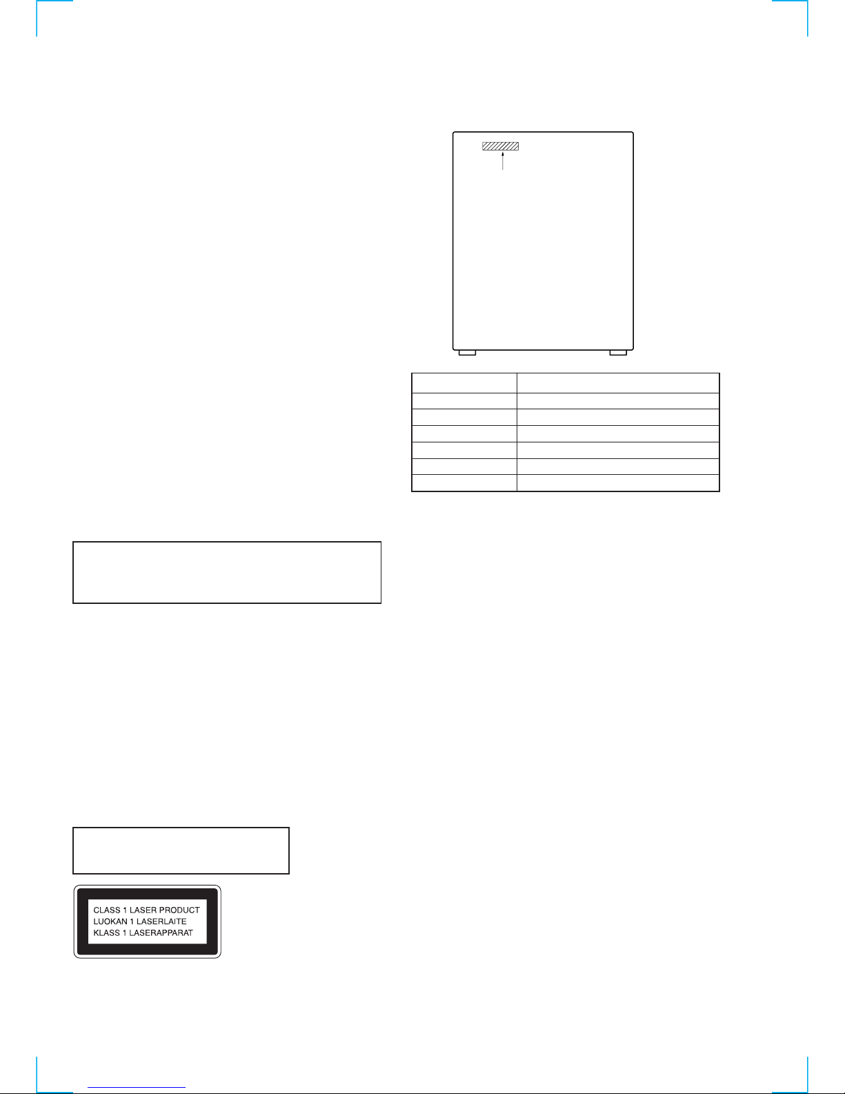
This appliance is classified as a CLASS 1 LASER product. The
CLASS 1 LASER PRODUCT MARKING is located on the rear
exterior.
The following caution label is located inside the unit.
Laser component in this product is capable
of emitting radiation exceeding the limit for
Class 1.
CAUTION
Use of controls or adjustments or performance of procedures
otherthan thosespecified herein mayresult inhazardous radiation
exposure.
Notes on chip component replacement
• Never reuse a disconnected chip component.
• Notice that the minus side of a tantalum capacitor may be
damaged by heat.
Flexible Circuit Board Repairing
• Keep the temperature of soldering iron around 270˚C
during repairing.
• Do not touch the soldering iron on the same conductor of the
circuit board (within 3 times).
• Be careful not to apply force on the conductor when soldering
or unsoldering.
AM tuner section
Tuning renge
European and Middle Eastern models:
531 – 1,602 kHz
(with the tuning interval set at 9 kHz)
Other models: 531 – 1,602 kHz
(with the tuning interval set at 9 kHz)
530 – 1,710 kHz
(with the tuning interval set at 10 kHz)
Antenna AM loop antenna,
External antenna terminals
Intermediate frequency 450 kHz
General
Power requirements
European model: 230 V AC, 50/60 Hz
Mexican model: 120V AC, 50/60 Hz
Australian model: 220 – 240 V AC, 50/60 Hz
Other models: 110 – 120 V or 220 – 240 V AC, 50/60 Hz Adjustable
with voltage selector
Power consumption
(HCD-DR330/DR3) 180W
(HCD-XB200) 135W
Dimensions(w/h/d) Approx. 355 ×425 ×442 mm
(14 ×163/4×171/2in) incl.
projecting parts and controls
Mass Approx. 13.1 kg (28 lb 14 oz.)
Supplied accessories AM loop antenna (1)
Remote RM-SG7B (1)
FM wire antenna (1)
Design and specifications are subject to change without notice
Parts No.
PARTS No. MODEL
4-222-140-0πXB200 : AEP, UK
4-222-141-0πXB200 : EE, CIS
4-222-142-0πDR3 : E, SP, AR
4-222-143-0πDR3 : AUS
4-222-144-0πDR3 : MX
4-222-145-0πDR330
MODEL IDENTIFICATION
• Abbreviation
SP : Singapore model
MX : Mexican model
AR : Argentina model
AUS : Australian model
EE : East European model

3
1. GENERAL ·········································································· 4
2. DISASSEMBLY
2-1. Top Cover ··········································································· 5
2-2. Front Panel Assy································································· 5
2-3. Main Section······································································· 6
2-4. Main Board ········································································· 6
2-5. CD Mechanism Deck Section ············································ 7
2-6. Tape Mechanism Deck Section ·········································· 7
2-7. Cassette Doors ···································································· 8
2-8. CD Chassis Assy ································································ 8
2-9. Base Unit ············································································ 9
2-10. Turn Table··········································································· 9
3. MECHANICAL ADJUSTMENTS ····························· 10
4. ELECTRICAL ADJUSTMENTS ······························· 10
5. DIAGRAMS
5-1. Ciecuit Boards Location··················································· 15
5-2. Block Diagrams ································································ 16
Main Section····································································· 16
Tuner/CD Section ····························································· 17
5-3. Printed Wiring Board Main Section ····························· 18
5-4. Schematic Diagram Main (1/3) Section ······················· 19
5-5. Schematic Diagram Main (2/3) Section ······················· 20
5-6. Schematic Diagram Main (3/3) Section ······················· 21
5-7. Printed Wiring Board AMP Section ····························· 22
5-8. Schematic Diagram AMP Section ································ 23
5-9. Printed Wiring Board CD Decoder Section ················· 24
5-10. Schematic Diagram CD Decoder Section ···················· 25
5-11. Printed Wiring Board Front Section ····························· 26
5-12. Schematic Diagram Front (1/2) Section ·······················27
5-13. Schematic Diagram Front (2/2) Section ·······················28
5-14. IC Pin Function Description············································· 29
5-15. IC Block Diagrams ··························································· 31
6. EXPLODED VIEWS
6-1. Top Cover Section ···························································· 33
6-2. CD Door Section ······························································ 34
6-3. Panel Section ···································································· 35
6-4. Main Section····································································· 36
6-5. CD Mechanism Section···················································· 37
6-6. Base Unit Section (KSM-213ECM)································· 38
7. ELECTRICAL PARTS LIST ······································· 39
TABLE OF CONTENTS

4
11/u(POWER) button
2TUNING MODE button
3STEREO/MONO button
4TUNER MEMORY button
5ENTER/NEXT button
6TUNER/BAND button
7TUNING – button
8TUNING + button
9FUNCTION button
!º VOLUME knob
!¡ PHONES jack
!™ ªbutton (DECK B)
!£ ·button (DECK B)
!¢ pbutton (DECK B)
!∞ 0button (DECK B)
!§ )button (DECK B)
!¶ Pbutton (DECK B)
!• rREC button (DECK B)
!ª CD SYNCHRO button
@º 0button (CD)
@¡ )button (CD)
@™ flbutton (CD)
@£ pbutton (CD)
@¢ REPEAT button
@∞ PLAY MODE button
@§ AMS knob
@¶ DISC SKIP button
@• EDIT button
@ª DISC 5 button
#º DISC 4 button
#¡ DISC 3 button
#™ DISC 2 button
#£ DISC 1 button
#¢ DIRECTION button
#∞ DOLBY NR button
#§ pbutton (DECK A)
SECTION 1
GENERAL
#¶ 0button (DECK A)
#• )button (DECK A)
#ª ªbutton (DECK A)
$º ·button (DECK A)
$¡ GROOVE button
$™ DBFB button
$£ SURROUND button
$¢ SPECTRUM ANALYZER button
$∞ DISPLAY/DEMO button
$§ ROCK button
$¶ POPS button
$• JAZZ button
$ª SALSA button
%º FLAT button
%¡ t/CLOCK SET button
%™ SLEEP button
%£ TIMER REC button
%¢ DAILY button
1 %¢%£ 23 54
$ª$• %º 6
8
9
7
!¡
%™
%¡
#™
#£
@™
0
$∞
$¢
!£!™
$¶$§
$º#ª
$™$¡ $£
@¡@º
!•
!ª
@£
!¶
!§!∞!¢
@∞
@¶
#º#¡ @¢
@§
@•
@ª
#∞#¢
#¶
#§ #•

5
SECTION 2
DISASSEMBLY
Note : Follow the disassembly procedure in the numerical order given.
2-1. TOP COVER
2-2. FRONT PANEL ASSY
2
Seven screws
1
Three screws
1
Three screws
3
Top cover
9
Front panel assy
6
Four screws
7
Screw
1
Connector
(to deck A)
2
Harness
(CN302)
4
Connector
(to deck B)
5
Connector
(CN702)
8
Board to board connector
(CN602)
(CN601)
3
Connector board
(CN11)

6
2-3. MAIN SECTION
2-4. MAIN BOARD
5
Two screws
4
Three screws
6
Two screws
7
Main section
2
Screw
3
Photo Socket board
1
Connector
(CN301)
4
Three screws
3
Four screws
1
Four screws
2
Three screws
5
Rear panel
6
Connector
(CN701)
8
Main board
7
Two screws

7
2-5. CD MECHANISM DECK SECTION
2-6. TAPE MECHANISM DECK
3
Four screws
4
CD mechanism
deck section
2
Holder, wire
1
Two screws
2
Six screws
1
Flexible flat cable
(to connector 16pin
on tape mechanism deck)
3
Tape mechanism deck

8
2-7. CASSETTE DOORS
2-8. CD CHASSIS ASSY
Cassette door (R)
(Note: Four claws are used.
)
Cassette door (L)
(Note: Four claws are used.)
1
Connector
(CN603)
8
Three screws
5
AMS knob
7
Washer
6
Nut
!º
Three screws
!¡
CD key board
!™
CD chassis assy
9
AMS board
3
Five screws
2
Connector
(CN606)
4
Remove the
six claws

9
2-9. BASE UNIT
2-10. TURNTABLE
Note:
When the disc table is installed, adjust the positions of
roller can and mark ”as shown in the figure, then set
to the groove of disc table.
5
Base uni
t
3
Yoke bracket
1
Connector
(CN02)
2
Connector
(CN01)
4
Boss
1
Screw
1
Screw
4
Turn tabl
e
3
Step screw
2
Bracket (BU)
A
A

10
2. Turn the adjustment screw and check output peaks. If the peaks
do not match for L-CH and R-CH, turn the adjustment screw
so that outputs match within 2 dB of peak.
L-CH
peak
R-CH
peak
screw
position
output
level within
2dB
L-CH
peak R-CH
peak
screw
position
within 2dB
Precaution
1. Clean the following parts with a denatured alcohol-moistened
swab:
record/playback head pinch rollers
erase head rubber belts
capstan idlers
2. Demagnetize the record/playback head with a head
demagnetizer.
3. Do not use a magnetized screwdriver for the adjustments.
4. After the adjustments, apply suitable locking compound to the
parts adjusted.
5. The adjustments should be performed with the rated power
supply voltage unless otherwise noted.
Torque Measurement
SECTION 3
MECHANICAL ADJUSTMENTS
Meter reading
40 to 70 g • cm
(0.56 - 0.97 oz • inch)
1 to 5 g • cm
(0.01 - 0.07 oz • inch)
55 to 140 g • cm
(0.76 - 1.94 oz • inch)
Torque
FWD
FWD
back tension
FF/REW
Torque meter
CQ-102C
CQ-102C
CQ-201B
SECTION 4
ELECTRICAL ADJUSTMENTS
1. Demagnetize the record/playback head with a head
demagnetizer.
2. Do not use a magnetized screwdriver for the adjustments.
3. After the adjustments, apply suitable locking compound to the
parts adjusted.
4. The adjustments should be performed with the rated power
supply voltage unless otherwise noted.
5. The adjustments should be performed in the order given in this
service manual. (As a general rule, playback circuit adjustment
should be completed before performing recording circuit
adjustment.)
6. The adjustments should be performed for both L-CH and R-
CH.
Record/Playback Head Azimuth Adjustment
(Deck A, Deck B)
Note: Perform this adjustments for both decks.
Procedure:
1. Mode : Playback
DECK SECTION 0 dB=0.775V
Tape
P-4-A100
WS-48B
Signal
10 kHz, –10 dB
3 kHz, 0 dB
Used for
Azimuth Adjustment
Tape Speed Adjustment
test tape
P-4-A100
(10kHz, –10dB)
set
SPEAKER
terminal (JK703)
level meter

11
test tape
P-4-A100
(10kHz, –10dB) SPEAKER
terminal (JK703)
(L-CH)
SPEAKER
terminal (JK703)
(R-CH)
oscilloscop
e
L
R
Waveform of oscilloscope
in phase 45˚ 90˚ 135˚ 180˚
good wrong
test tape
WS-48B
(3kHz, 0dB)
set
SPEAKER
terminal (JK703)
frequency counte
r
+
–
IC603
CN603
SFR601
TAPE SPEED
Adjustment screws
PB head (deckA)
or REC/PB head (deck B)
3. Mode: Playback Tape Speed Adjustment (Deck A)
Procedure:
1. Mode: Playback
2. Adjust the SFR601 so that the frequency counter reads 3,000
Hz ± 90Hz.
Adjustment Location: FRONT board
Sample Value of Wow and flutter
W. RMS (JIS) within 0.3%
(test tape: WS-48B)
Adjustment Location: FRONT board
[FRONT BOARD] — Component side —
4. After the adjustments, apply suitable locking compound to the
parts adjusted.
Adjustment Location:
Remove the cassette lid before adjustment (See page 8)

12
TUNER SECTION 0 dB=1µV
AMTuningVoltage Adjustment
Procedure:
1. Set the reception frequency of the unit to 530 kHz.
2. Adjust L105 for 1.2 ± 0.05 V reading on the DC voltmeter.
3. Set the reception frequency of the unit to 1,710 kHz.
4. Confirm that the voltage reading on the DC voltmeter is within
8.0 ± 0.5 V.
Adjustment Location: MAIN board (See page 13)
AMTracking Adjustment
Procedure:
1. Tune the set to 600 kHz.
2. Set the output ofAM RF SSG so that the input level of the set
will become 60 dB (µV/m).
3. Adjust L104 so that when the waveform on the oscilloscope is
maximum, no noise appears.
4. Tune the set to 1,400 kHz.
5. Adjust TC102 so that when the waveform on the oscilloscope
is maximum, no noise appears.
• Repeat the procedures in each adjustment several times, and the
tracking adjustment should be finally done by the trimmer
capacitors.
Adjustment Location: MAIN board (See page 13)
Main board
TP1
G
VT
DC voltmete
r
+
–
AM RF SSG
loop antenna
set
loop antenna
(Supplied accessories)
60 cm AM ANTENNA
terminal (TM1)
30% amplitude
modulation by
400 Hz signal Field strength dB (
µ
V/m) =SSG output level dB (
µ
V/m) –26 dB.

13
FMTuned Level Adjustment
Procedure:
1. Supply a 28 dB 98 MHz signal from theANTENNA terminal.
2. Tune the set to 98 MHz.
3. Adjust SFR101 to the point (moment) when the TUNED
indicator will change from going off to going on.
Adjustment Location: MAIN board
Adjustment Location
[MAIN BOARD] — Component side —
FM RF SSG
75
Ω
coaxial
Carrier frequency : 98 MHz
Modulation :AUDIO 1 kHz, 75 kHz
deviation (100%)
Output level :28 dB (at 75 W open)
FM ANTENNA terminal
(JK101)
set
L104
L105
TP1
TC102
AM Tracking
AM Tuning Voltage
FM Tuned Level
IC102
SFR101 JK101

14
CD SECTION
Note:
1. CD Block is basically constructed to operate without
adjustment. Therefore, check each item in order given.
2. UseYEDS-18 disc (3-702-101-01) unless otherwise indicated.
3. Use an oscilloscope with more than 10MΩimpedance.
4. Clean the object lens by an applicator with neutral detergent
when the signal level is low than specified value with the
following checks.
5. Adjust the focus bias adjustment when optical pick-up block is
replaced.
RF Level Check
Procedure :
1. Connect oscilloscope to test point TP01 on CD DECODER
board.
2. Turned Power switch on.
3. Put disc (YEDS-18) in and playback.
4. Confirm that oscilloscope waveform is clear and check RF
signal level is correct or not.
Note: Clear RF signal waveform means that the shape “◊” can be
clearly distinguished at the center of the waveform.
Adjustment Location:
[CD DECODER BOARD] — Component side —
CD DECODER
board oscilloscope
RF
VC
TP01
VOLT/DIV: 200 m
V
TIME/DIV: 500 nS
level: 1.0 Vp-p
+0.3
–0.2
TP01
(VC)

1515
SECTION 5
DIAGRAMS
5-1. CIRCUIT BOARDS LOCATION •Waveform
1
2
3
4
IC103 @™
IC601 !§
IC01 #£
IC02 &¡
5
L809 5
6
L809 6
3.6 Vp-p
7.2 MHz
3.8 Vp-p
6 MHz
1.3 Vp-p
5.0 Vp-p
16.9345 MHz
32 Vp-p
111.7 kHz
96 Vp-p
111.0 kHz
MAIN BOARD
FRONT BOARD
CD DECODE BOARD
For schematic diagrams.
Note:
• All capacitors are in µF unless otherwise noted. pF: µµF
50 WV or less are not indicated except for electrolytics
and tantalums.
• All resistors are in Ωand 1/4W or less unless otherwise
specified.
• % : indicates tolerance.
•¢: internal component.
•2: nonflammable resistor.
•1: fusible resistor.
•C: panel designation.
•U: B+ Line.
•V: B– Line.
•H: adjustment for repair.
• Voltages and waveforms are dc with respect to ground
under no-signal (detuned) conditions.
• Voltages aretaken withaVOM(Inputimpedance 10MΩ).
Voltage variations may be noted due to normal produc-
tion tolerances.
• Waveforms are taken with a oscilloscope.
• Circled numbers refer to waveforms.
• Signal path.
F: FM
f: AM
E: PB (DECK A)
d: PB (DECK B)
G: REC (DECK B)
J: CD
g: MD/VIDEO
i: PHONO
For printed wiring boards.
Note:
•X: parts extracted from the component side.
•®:Through hole.
•¢: internal component.
•b: Pattern from the side which enables seeing.
THIS NOTE IS COMMON FOR PRINTED WIRING
BOARDS AND SCHEMATIC DIAGRAMS.
(In addition to this necessary note is printed in each
block.)
• Indication of transistor.
• Abbreviation
SP : Singapore model
MX : Mexican model
AR : Argentina model
AUS : Australian model
MAIN board
CONNECTOR board
TR board
LED board
CD KEY board
CD SW board
POWER (AMP) board
POWER SUPPLY board
AC SWITCH board
PHOTO SOCKET board
REM board
AMS board
VR board
H/P board
FRONT board
MOTOR board
DISC NO board CD DECODE board
MOTOR (6P)(C) boar
d
CD SENSOR board
B
This is omitted.
CE
Q
The components identified by mark !or dotted
line with mark !are critical for safety.
Replace only with part number specified.

HCD-DR3/DR330/XB200
1616
5-2. BLOCK DIAGRAM
MAIN SECTION
: FM
: CD
• Signal Path
• RCH is omitted • Abbreviation
SP:Singapore
AR:Argentina
C
CD
SECTION
TU L
ST IND
TU MUTE
DO1
Q709
MUTE
14 7
4
POWER AMP
IC701
SPEAKER
RELAY
DRIVE
Q711
1
26
IC702
RL701
SPEAKER
PHONES
JK703
JK701
SCOR
SENS1
SQSO
XLAT
SQCK
CLK
CE
STB
91
STB
100
SCLK
98
SDATA OUT
95
DATA
97
SQCK
94
XLAT
96
SQSO
11
SENS1
27
SCOR
99
SDATA IN
9
MD MUTE
73
FM ST IND
2
SYSTEM MUTE
1
POWER OUT
LED DRIVE
IC603
1
2
3
88
LATCH
DI
CLK
RESET
SWITCH
POWER
DOWN DET
Q601
Q602
LED610-615
X2
17
X1
16
VR UP
81
X601
6MHz
VR DOWN
82
VR601
VOLUME
CD DOOR
79
AB
S653
DOOR SW
2
3
RM601
REMOTE
CONTROL
RECEIVER
KEY
MATRIX
S601-651
K0 K4
FLD601
SYSTEM CONTROLLER/
FLD DRIVER
IC601
-5.6V
REG
Q308
SITCHING
Q309
+7.5V
REG
Q702
CD +7.5V
+12V
REG
Q701
RECT
D701
AC OFF
DET
Q704 705
RECT
D705-708
220-240V
110-120V
-27V
REG
Q703
IC701 B+
AC IN
AC IN
T001
S001
AC5.4V
AC5.4V
16
A
TUNER
SECTION
(PAGE 17)
(PAGE 17)
(PAGE 17)
: PB (DECK A)
: PB (DECK B)
: REC (DECK B)
CLK
DI
87
LOCK
BUS REGISTER
IC607
REC MUTE
13
PLAY MUTE
14 A/B
11 BIAS
12
SI
2CLK
3
STB
1
DI
CLK
4PLAY
5
SOL A
6
SOL B
SOL A
DRIVE
Q612,615
M+12V
SWITCH
Q610,613
M+12V
SOL B
DRIVE
Q611,614
SHIFT REGISTER
IC606
CK
2
S/L
1
QH
9
CLK 3REC A
5
PHOTO A
11
A MODE SW
13A HALF
6
PHOTO B
12
B MODE SW
14B HALF
MECHA
BLOCK
D715
-5.6V
45 3019 23
Q'S
10
SCOR
DATA IN
DATA
SENS2
LOCK
75
SENS2
74
AMS
86
S/L
80
DATA IN
HP901
PB
HEAD
TAPE A
HRP901
REC/PB
HEAD
TAPE B
R CHR CH
R CH
PLAY/REC
CONTROL
Q803,805
PLAY/REC
CONTROL
DRIVE
Q823
PLAY/REC
CONTROL
D802
L609
BIAS OSC
BIAS
OSC
HE901
ERASE
HEAD
5
7
6PB OUT
A/B
2
3
EQ AMP
IC801
Q816,817
D803
Q801
BIAS
SWITCH
Q829,830
Q807
PHONO
JK201
R
LIC202
R CH
BIAS
TRAP
L805
SFR807
9
SFR807
SFR801
SFR803
14
10
13
11
12
8 1
SW
VALC
REC AMP
PB/REC AMP
IC802
Q811
BUFFER
D807 Q813
MUTE
CONT
Q825,826
16
14
DOLBY AMP
IC803
12
9
11
5
D808
SFR805
Q822
PB
MUTE
Q815
MUTE
D811
MD/VIDEO
IN R
L
R CH
BIAS
+12V +12V
Q833
Q809
REC
MUTE
Q831
AMS
Q832
TAPE PLAY
7
D804
B
CD
SECTION
IC303
MD/VIDEO
MD (HI)
Q209
MUTE
8
6
10
12
9
11
IC203
Q210 Q207
Q201
AMP
Q204
MUTE L1 (CD)
2L4 (AUX)
9L3 (TAPE)
8L2 (TUNER)
7L (REC)
3
13 14
11
VR
DATA CLK
SELECTOR
IC201
DATA
4
SURROUND OUT
6
DBFB ON/OFF
5
DBFB H/L
Q306
SURROUND
CONTROL
Q305
Q301
Q303
IC301 IC302
MUTE
Q707
R CH
+12V
Q708
MD/VIDEO OUT
R
L
R CH
JK201
LED DRIVE
IC602
2
45LED
DRIVE
DI
CLK
Q608,609
LED605-608
LED516
6
11
14
16
.
17
.
7
9
11
14
.
43
16 DOLBY OUT
LED601-603
7 8 85
4REC B
12
13
4
5
8
6
10
12
1
3
9
11
26
VACS
10
SPEANA H/L
25
SPEANA 2
24
SPEANA 1
IC604
Q607
CLK
DI
100
SCLK CLK
93
CE CE
CD ENCODER A
83
CD ENCODER B
84
VR602
CD ENCODER
AB
RESET
12
POWER DOWN
13
REMOTE
29
VCCVCC
47 50 52 68
.
P1 P21 G1 G16
FLUORESCENT
INDICATOR TUBE
MUTE
SWITCH
Q713
+12V
IC701 B-
-30V
+5.6V
REG
Q310
+12V
(CASSETTE)
D+12V
(MOTOR)
+12V
(BIAS)
D601
D602
VCC
+12V
(TUNER)
+5.6V
µCON B+
CD L
Q205
: MD
FOK
CNIN
76
FOK
28
CNIN
UP SW
77
TABLE SENSOR
78
S06
UP SW
TABLE
SENSOR
SENS01
F702
F703
F702
EXCEPT E,SP,AR
E,SP,AR MODEL
AC VOLTAGE

HCD-DR3/DR330/XB200
1717
TUNER/CD SECTION
CE
16 10
6
5
3
22
1
PLL
IC103
FM
XO
XI CLK
DO
CE
CLK
DO
OPTICAL PICK-UP
BLOCK
APC
Q01 41
VCC
VC
LD
GND
A
C
B
E
F
FOCUS
COIL
F+
F
T+
T
TRACKING
COIL
36
37
42
39
38
51
APC
FOCUS PHASE
COMPENSATION
DECODER
SERIAL/
PARALLEL
CONVERTER
FE
AMP
RF
AMP
IIL
TTL
TTL
IIL
COMAND
VC
TRACKING PHASE
COMPENSATION
LD
PD
E
F
PD1
PD2
6
25
24
21
20
23
22
33
27
SENS1
RFO
FOK
C OUT
DATA
XLT
CLK
XRST
13
FEO TAO
IC03
T.T/TRAY MOTOR
DRIVER
CD RF/SERVO
PROSSESOR
IC01 (1/2)
15
25
T IN
16
17
18
VR
PD
PD
12
11
14
13
27
F IN
6
SL IN
9
IN1
F+
F
T+
T
SL+
SL
SP+
SP
M
M
MOTOR
M102
SLED
MOTOR
M101
SPINDOL
EFM
DEMO.
XRST
CLV
SERVO
DIGITAL
CLV
D/A
I/F
SUB CODE
PROSSESOR
CPU I/F
7 9 4 5 6 6257
MDP
SENS
SCOR
SQSO
SQCK
CLOCK
DATA
CLK
XLT
DAT
SE
CIN
FOK
RF
SERIAL
I/F
PWM 67
70
71
NL
XTA1
XTA0 X701
MUTE
R-CH
CD DIGITAL
SIGNAL PROCESSOR
IC02
16
:FM
:CD
• SIGNAL PATH
14
7
8
4
2
1
6
10
DETECTOR
16
OSC
FM
75Ω
AM
ANTENNA
JK101 3
8RF MIX 1
4
FM FRONT END
FE101
RF IF
AMP
Q101
CF101
10.7MHz CF102
10.7MHz
L105
MW OSC
IF
G
VT
L104
AM ANT
AM RF
AMP
Q108
MPX
16
FM IF
1
OSC
23
AFC
22 AM RF
21
FM
IF
AM OUT
19
FM
DET
AM/FM
IF BUFF
AM
OSC AM
MIX
AM
DET
SMET
20
CF103
450kHz
MUTE
AGC
AM
IF
DECODER 13
L
14
R
4
2
T102
AM IFT
8
FM DET CF104
10.7MHz
R CH
FM/AM MPX
IC102
FM
TUNED
LEVEL
PD1
18
X201
7.2MHz
FM B+
7
TUB+
+12V
Q114
ST MONO
12
15
AM
OSC/FMSD
24
B+
11
SD IN 9
FM ST
TU LED
6
12
IF IN
SD SPEED
7
ST IND
10
IF BUFF
MUTE
Q117
TU L
ST IND
TU MUTE
DO 1
A
MAIN
SECTION
(PAGE 16)
D
5
LD
PD
F/T COIL
SL/SP MOTOR
7
3
OUT1
OUT2
M
MOTOR
TABLE
23
SP IN
1
IN2
IC701 (2/2)
XRST
6
Q702
12 LED CONT
13
12
MIN1
MIN2
4
MUTE
3
CLOK
1
STB
IC04
SHIFT REGISTER
35
18
11
10
12
13
14
79
21
15
SPOA
STOP
SWITCH
8
XLAT
CLOCK
GEN.
PWM 74
NR MUTE
Q09
CD L
SCOR
SENS1
SQSO
XLAT
SQCK
DATA
CE
STB
CLK
C
MAIN
SECTION
:AM
• RCH is omitted
SFR101
CNIN
FOK
OSC
VT G
TP2
TP1
2
DATA
26
SENS2
19
LOCK
16.9344MHz
2
L MUTE
53
D OUT DIGITAL
OUT
PH01
B
MAIN
SECTION
DATA IN
D107
4
DI DI
DI
IC05
TABLE
MOTOR DRIVE
12 LED CONT
DRIVER
LED
DISC NO
D06
Q04
REG
Q03
+5V SW
B+
+5.6V
VCC
SENS2
LOCK
MUTE
SWITCH
Q11,13
(PAGE 16)
(PAGE 16)

HCD-DR3/DR330/XB200
1818
5-3. PRINTEDWIRING BOARD MAIN SECTION • Refer to page 15 for Circuit Boards Location.
Ref. No. Location
• Semiconductor Location
Ref. No. Location
D07 J-11
D08 J-10
D09 J-9
D10 J-8
D101 C-2
D102 C-2
D103 A-2
D104 A-2
D107 B-3
D109 C-5
D110 B-8
D111 A-8
D301 E-4
D302 D-10
D303 I-4
D304 B-11
D305 D-3
D306 E-7
D307 A-9
D308 A-9
D309 C-11
D310 C-11
D802 I-9
D803 I-9
D804 F-8
D805 C-11
D806 D-11
D807 E-7
D808 E-7
D811 I-10
D812 F-12
IC102 B-6
IC103 D-3
IC201 E-4
IC202 H-3
IC203 F-3
IC301 F-4
IC302 H-4
IC303 B-9
IC801 G-8
IC802 F-8
IC803 G-6
Q101 B-5
Q108 A-3
Q114 C-3
Q116 B-7
Q117 A-7
Q201 D-9
Q202 E-7
Q203 C-9
Q204 D-8
Q205 C-10
Q206 H-8
Q207 E-3
Q208 E-3
Q209 E-3
Q210 D-3
Q301 H-4
Q302 G-5
Q303 H-4
Q304 G-5
Q305 G-4
Q306 D-10
Q308 I-4
Q309 I-4
Q310 A-10
Q801 F-10
Q802 G-9
Q803 G-10
Q804 G-10
Q805 G-10
Q806 G-10
Q807 F-8
Q808 G-7
Q809 H-9
Q810 F-6
Q811 G-7
Q812 F-6
Q813 H-7
Q814 F-6
Q815 H-6
Q816 I-10
Q817 I-10
Q822 E-6
Q825 G-10
Q826 F-10
Q829 E-11
Q830 E-11
Q831 D-11
Q832 D-11
Q833 F-12
MAIN BOARD
LED BOARD
JK101
ANTENNA
AM
FM
RL
RL
RL
IN
MD/VIDEO
PHONO IN
OUT
16
JK201
TO
AMP BOARD
CN701
(Page 22)
C
TO
CD DECODER
BOARD
CN03
(Page 24)
D
TO
FRONT BOARD
CN601
(Page 26)
B
TO
FRONT BOARD
CN602
(Page 26)
A
1-674-636-
11
(11)
(4144268510)
1-674-637-(CASSETTE BOX BACK LIGHT)
11
(11)
(4144268520)
1
2
1
1
1
1
1
3
1
13
8
916
18
916
5
2
2
2
2
1
14
58
1
1
1
1
1
1
14
15
11
12 22
458
12
1324
28
7
814
4
58
1
1
18
916
12
1
1
3
6
4
58
58
14
HRP901
RECORD/
PLAYBACK
HEAD
HP901
PLAYBACK
HEAD
HE901
ERASE
HEAD
X
B DECK
A DECK
1
2
1
1
1
16
1
16
2
3
4
5
2
3
D104
L104
L105 L109
L108
L114
D103
D107 C114
C179
C187
C113
C116
C115
C188
C189
C129
C154
C121
C126
C127
C122
C161
C198 C140
C142
C141
C160 C257
C132
C139
C256
C117
C163
C120
C128
C138
C137
C164
C131
C130
C125
C133
C333
C343
C339
D309
D805
D310
C350
C149
C124
C123
C151
C135
C177
C159
C194
C195
C199
Q210
Q208
Q207 R268
Q822
Q812
Q814
Q811
Q202
Q306
C152
C327
C219
C223 R267
C312
C346
C301
R318
R322
C320
C302
R324 R311
R314
R303
R307
R320
C305
C316
R305
C314
R316
C309 C307
R301
IC301
C222 C311
C220
C214
C213
C250
C244
C240
C239
C232
C236
C858
C864
C857
C860
C862 C866
C230
C228
C234
C328
C876
D808
D807
C246
D305
C155
C148
C143
L113
C108
C144
C150
C165
C185
R155
R104
R112
R137
R136
R116
R115
R140
R135
R260
R229
R254
R255
R352
R302
C302
C310
R306
R243
R245
C243
C308
C306
R354
R256
R253
R228
R355
R891
R887
R854
R870
R868
R831
R838
R847
R844 R237
R239
R233
R249
R235
R828
R825
R819
R841
R839
Q801
Q805Q803
Q806
Q802
Q804
R804
R893 R802
R827
R805
R806
R901
R896
R899
R808
R895
R807
R897
R809
R811
R810
R800A R820
R527
R867
R883
R873
R882
R878
R877
R875
R863
R861
R326
R332
R312
R864
R862 R866
R874
R824
R855
R881
R818
Q816
Q823
Q809
Q206
Q813
Q815
Q817
R894
D811
D802
D803
CN802
CN811 CN812
R817
R905
R821
SFR803
SFR806
SFR804
SFR805
SFR801
SFR807
SFR802
SFR808
IC801
C829
C819
C815
C811
C825
C820
C806
C803
C821
C896
C837
C835
C845
C807
C813
C822
C801
C802
CN803
C886
C881
C877
C887
C805
C818
C824
C853 C865
C869
C861
C893
C907
C337
C334 C315
C313
C249
C321
C319
C318
C323
C322
C205
C218
C217
IC302
IC202
C248
C201
C204
C338
C335 C336
D303
C324 C325
CN801
CN302
C816
C814
C809
C902
C875
C882
C823
R837
R892
R236
R888
R858
R845
R853 R846
R825
R250
R330
R117
R133
R134
R714
R139
R132
Q108
TC102 GDS
R114
R113
R118
R119
C146
R106 R167
R144
R151
R118 R123
R121
R175
R157
R344
R141
R142
R241
R231
R240
R926
R843
R353
L806
C922
C884
C839 C849
C838
C848
C833
C345 C227
C231
C233
C828
C847
C906 C237
Q205
Q832
R242
R143
R339
R337
R889
R172
R130
D110 R131
R127R129
R120
R173
SFR101
R180
R147 R107
R105
D109L106
FE101
C157
C156
C162
C158
CF101
CF102
CF103
CF104
Q101
Q114
T102
R124
Q117
Q116
B
B
E
E
BE
R156
R128
R126
IC102
IC103
IC201
TP1
X101
D102
D101
C186S
S
GD
D
C196
C260
C226
C242
C235
C197
G
C221
B
B
E
EB
B
B
B
B
B
E
E
E
E
E
E
B
E
B
E
D301
R259
R265
R266
R264
R263
R258
R334
R234
R238
R848 R849
R842
R830 R829
R232
Q204
R836
C867
C825
C894 Q810
D306
D111 D307
D304
D308
IC303
C347
C330 C341
C340
R338
R138
R346
R345
L301
L302
C342
Q310
B
E
CN602
CN601
R925
R924
R917
R916
R918
R919
R921
R920
R923
R922
C905
C925
D302
S
D
G
C903
C904
B
B
E
E
Q831 D806
Q833
Q830
Q829
B
B
B
E
E
E
R912
R913
R911
R931
R930
R906
D812
CN809
C841
C842
R833
R835
R815
R814R832
R840 R834 C883
C846
C840
IC802
C834
C827 C836
L804
C856
R329
R333
Q203
Q201
B
B
E
E
C238 C329
C229 L803
G
D
S
Q807
B
EL801
C817
C826
C831
C851
D804
R823
R803
R907
Q825
B
B
BB
B
B
B
B
B
BE
E
E
E
E
E
E
E
B
B
E
E
E
E
Q826
B
E
R801
L805
R890
C885
L809
C888
L808 C921
R898
C880
E
E
E
B
B
B
CN808
C897
C808
C901
C812
C804
R812
R816 R822
Q808
R251
R252
R225
R227
Q209
IC203 R310
R262
R261
R309
R244
R308
C247
R351
C241
R304
C304
R850
C830
C832
C895
C855
C800A
C854
R856
R872 R860
R884
R859
C870
L802
R826
GND302
GND301
CN302 D10 D09 D08 D07
R448
R851
C891
R328
C863
C868
C908
C859
R871
R857
R915
R865
IC803
R869
CN401
CN301
CN807
R914
R880
R876
C892
C216
R208 C210
C212
R214
R219
R313
R315
R323
R331
R212
R206
C206
R204 R202
R201
R213 R215 R216
R218
R222
R223
R205 R221
R224
C202
C207 C209
C208
C252
R220
R210
C255 R350
R347
R247
R245
R327
B
B
E
E
Q308 Q309
R357 R321
R317
C317
R246
R325
R248
Q302
Q303
B
E
B
E
R319
C215
C211
R211
R209
C251 R356
Q305
Q301
R217
GSD
C203
R207
R203
B
E
B
E
Q304
2
1
XB200
MODEL
XB200
MODEL
XB200
MODEL
C107
DR3/DR330
MODEL
12
A
B
C
D
E
F
G
H
I
J
3456789101112

HCD-DR3/DR330/XB200
1919
5-4. SCHEMATIC DIAGRAM MAIN (1/3) SECTION • Refer to page 15 for Waveform. • Refer to page 31 for IC Block Diagrams.

HCD-DR3/DR330/XB200
2020
5-5. SCHEMATIC DIAGRAM MAIN (2/3) SECTION • Refer to page 15 forWaveform. • Refer to page 18 for Printed Wiring Board.
Other manuals for HCD-DR3
3
This manual suits for next models
2
Table of contents
Other Sony Stereo System manuals

Sony
Sony DHC-FL3 User manual

Sony
Sony MHC-RG40 - Mini Hi-fi Component System User manual

Sony
Sony 4548736019614 User manual

Sony
Sony CMT-C7NT User manual

Sony
Sony LBT-D590 - Compact Hifi Stereo System User manual

Sony
Sony LBT-D170 User manual

Sony
Sony MHC-GN700 User manual

Sony
Sony LBT-G3000 User manual

Sony
Sony Psyc ZS-YN7 User manual

Sony
Sony CMT-SX7 User guide