Sony HCD-GZR888DA User manual

SERVICE MANUAL
Sony Corporation
Published by Sony Techno Create Corporation
HCD-GZR888DA/
GZR999DA
HCD-GZR888DA/GZR999DA: E3, E4, PH, SP Model
DVD DECK RECEIVER
HCD-GZR999DA: E2, E51, MX Model
DVD RECEIVER
9-893-138-01
2011C04-1
© 2011.03
E Model
Ver. 1.0 2011.03
• HCD-GZR888DA/GZR999DA are the tuner,
deck, DVD and amplifier section in MHC-
GZR888DA/GZR999DA. Photo: HCD-GZR999DA
SPECIFICATIONS
DVD
Section
Model Name Using Similar Mechanism HCD-GZR777DA
DVD Mechanism Type CDM74HFVX-DVBU101
Optical Pick-up Name KHM-313CAB
Tape Deck
Section
Model Name Using Similar Mechanism HCD-GZR777DA
Tape Transport Mechanism Type CFP42608
Amplifier section
The following measured at AC 127 V, 60 Hz
(Mexican model)
The following measured at AC 120 V, 220 V,
240 V, 50/60 Hz (Other models)
MHC-GZR999DA
Power output (rated):
135 W + 135 W (at 6 Ω, 1 kHz, 1%
THD, at LINK MODE)
RMS output power (reference)
Front speaker:
210 W + 210 W (per channel at 8 Ω,
1 kHz)
Satellite speaker:
90 W + 90 W (per channel at 24 Ω,
1 kHz)
Subwoofer:
240 W (at 6 Ω, 100 Hz)
MHC-GZR888DA
Power output (rated):
125 W + 125 W (at 6 Ω, 1 kHz, 1%
THD, at LINK MODE)
RMS output power (reference)
Front speaker:
210 W + 210 W (per channel at 8 Ω,
1 kHz)
Satellite speaker:
90 W + 90 W (per channel at 24 Ω,
1 kHz)
– Continued on next page –
• Abbreviation
E2 : 120V AC area in E model
E3 : 240V AC area in E model
E4 : 110 – 120V/220 – 240V AC area in E model
E51 : Chilean and Peruvian models
MX : Mexican model
PH : Philippines model
SP : Singapore model

HCD-GZR888DA/GZR999DA
2
SAFETY-RELATED COMPONENT WARNING!
COMPONENTS IDENTIFIED BY MARK 0OR DOTTED LINE
WITH MARK 0ON THE SCHEMATIC DIAGRAMS AND IN
THE PARTS LIST ARE CRITICAL TO SAFE OPERATION.
REPLACE THESE COMPONENTS WITH SONY PARTS
WHOSE PART NUMBERS APPEAR AS SHOWN IN THIS
MANUAL OR IN SUPPLEMENTS PUBLISHED BY SONY.
Inputs
VIDEO/SAT VIDEO IN (phono jack):
1 Vp-p, 75 Ω
VIDEO/SAT AUDIO IN L/R (phono jacks):
voltage 250/450 mV, impedance
47 kΩ
MIC (phone jack):
sensitivity 1 mV, impedance 10 kΩ
Outputs
VIDEO OUT (phono jack):
max. output level 1 Vp-p, unbalanced,
Sync negative, load impedance 75 Ω
COMPONENT VIDEO OUT
Y: 1 Vp-p, 75 Ω
PB: 0.7 Vp-p, 75 Ω
PR: 0.7 Vp-p, 75 Ω
DVD DIGITAL OUT (Square optical
connector jack, rear panel):
Wavelength 650 nm
PHONES (stereo mini jack):
accepts headphones of 8 Ωor more
SUBWOOFER OUT (MHC-GZR888DA):
Voltage 1 V, impedance 1 kΩ
FRONT SPEAKERS:
Use only the supplied speaker
SS-GZR999D.
SATELLITE SPEAKERS:
Use only the supplied speaker
SS-RSZ999D.
SUBWOOFER (MHC-GZR999DA):
Use only the supplied subwoofer
SS-WGR999D.
(USB) port: Type A
Maximum current:
500 mA
Disc player section
System:
Compact disc and digital audio and
video system
Laser Diode Properties
Emission Duration: Continuous
Laser Output*: Less than 44.6μW
* This output is the value measurement
at a distance of 200mm from the
objective lens surface on the Optical
Pick-up Block with 7mm aperture.
Frequency response
DVD (PCM 48 kHz): 2 Hz – 22 kHz
(±1 dB)
CD: 2 Hz – 20 kHz (±0.5 dB)
Video color system format
Latin American models: NTSC
Other models: NTSC and PAL
Tape deck section (except for Latin
American models)
Recording system:
4-track 2-channel, stereo
Tuner section
FM stereo, FM/AM superheterodyne tuner
FM tuner section
Tuning range:
87.5 MHz – 108.0 MHz (50 kHz step)
Antenna:
FM lead antenna
Antenna terminals:
75 Ωunbalanced
Intermediate frequency:
10.7 MHz
AM tuner section
Tuning range
Latin American models:
530 kHz – 1,710 kHz (10 kHz step)
531 kHz – 1,710 kHz (9 kHz step)
Other models:
531 kHz – 1,602 kHz (9 kHz step)
530 kHz – 1,610 kHz (10 kHz step)
Antenna:
AM loop antenna
Antenna terminals:
External antenna terminal
Intermediate frequency:
450 kHz
General
Power requirements
Mexican model:
AC 127 V, 60 Hz
Other models:
AC 120 V, 220 V, 230 V – 240 V,
50/60 Hz, adjustable with voltage
selector
Power consumption
MHC-GZR999DA: 215 W
MHC-GZR888DA: 170 W
Dimensions (W/H/D) (excl. speakers):
Approx. 280 mm ×325 mm ×
430 mm
Mass (excl. speakers)
MHC-GZR999DA: Approx. 12.8 kg
(Latin American models), approx.
13.2 kg (other models)
MHC-GZR888DA: Approx. 12.8 kg
Supplied accessories:
Remote Commander (1)
AM loop antenna (1)
FM lead antenna (1)
Speaker pads (MHC-GZR999DA
(20), MHC-GZR888DA (16))
Speaker cords (2)
Microphone (1) (Philippine model
only)
R6 (Size AA) batteries (2)
Design and specifications are subject to
change without notice.

HCD-GZR888DA/GZR999DA
3
UNLEADED SOLDER
Boards requiring use of unleaded solder are printed with the lead-
free mark (LF) indicating the solder contains no lead.
(Caution: Some printed circuit boards may not come printed with
the lead free mark due to their particular size)
: LEAD FREE MARK
Unleaded solder has the following characteristics.
• Unleaded solder melts at a temperature about 40 °C higher
than ordinary solder.
Ordinary soldering irons can be used but the iron tip has to be
applied to the solder joint for a slightly longer time.
Soldering irons using a temperature regulator should be set to
about 350 °C.
Caution: The printed pattern (copper foil) may peel away if
the heated tip is applied for too long, so be careful!
• Strong viscosity
Unleaded solder is more viscous (sticky, less prone to flow)
than ordinary solder so use caution not to let solder bridges
occur such as on IC pins, etc.
• Usable with ordinary solder
It is best to use only unleaded solder but unleaded solder may
also be added to ordinary solder.
NOTES ON CHIP COMPONENT REPLACEMENT
• Never reuse a disconnected chip component.
• Notice that the minus side of a tantalum capacitor may be dam-
aged by heat.
FLEXIBLE CIRCUIT BOARD REPAIRING
• Keep the temperature of soldering iron around 270 °C during
repairing.
• Do not touch the soldering iron on the same conductor of the
circuit board (within 3 times).
• Be careful not to apply force on the conductor when soldering
or unsoldering.
CAUTION
Use of controls or adjustments or performance of procedures
other than those specified herein may result in hazardous radia-
tion exposure.
NOTES ON HANDLING THE OPTICAL PICK-UP
BLOCK OR BASE UNIT
The laser diode in the optical pick-up block may suffer electro-
static break-down because of the potential difference generated by
the charged electrostatic load, etc. on clothing and the human body.
During repair, pay attention to electrostatic break-down and also
use the procedure in the printed matter which is included in the
repair parts.
The flexible board is easily damaged and should be handled with
care.
NOTES ON LASER DIODE EMISSION CHECK
The laser beam on this model is concentrated so as to be focused
on the disc reflective surface by the objective lens in the optical
pickup block. Therefore, when checking the laser diode emission,
observe from more than 30 cm away from the objective lens.
Laser component in this product is capable of emitting radiation
exceeding the limit for Class 1.
This appliance is classified as
a CLASS 1 LASER product.
This marking is located on the
rear exterior.

HCD-GZR888DA/GZR999DA
4
• Abbreviation
E2 : 120V AC area in E model
E3 : 240V AC area in E model
E4 : 110 – 120V/220 – 240V AC area in E model
E12 : 220 – 240V AC area in E model
E51 : Chilean and Peruvian models
MX : Mexican model
PH : Philippines model
SP : Singapore model
Model Part No.
GZR888DA: E3 model 4-278-558-0[]
GZR888DA: E4 model 4-278-558-1[]
GZR888DA: E12 model 4-278-558-2[]
GZR888DA: SP model 4-278-558-4[]
GZR999DA: E3 model 4-278-559-0[]
GZR999DA: E4 model 4-278-559-1[]
GZR999DA: SP model 4-278-559-3[]
GZR999DA: PH model 4-278-559-4[]
GZR999DA: E2, E51 models 4-278-559-5[]
GZR999DA: MX model 4-278-559-6[]
MODEL IDENTIFICATION
– Back Panel –
Parts No.

HCD-GZR888DA/GZR999DA
5
1. SERVICING NOTES ............................................. 6
2. DISASSEMBLY
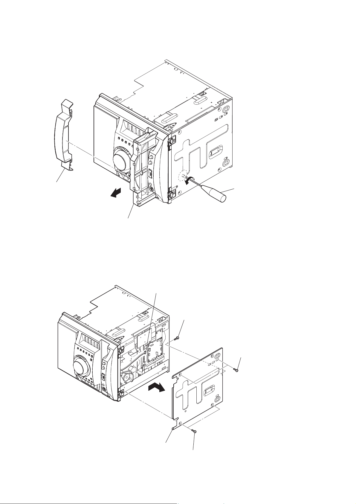
2-1. Case (Side-L), Case (Side-R).......................................... 9
2-2. Top Panel Section ........................................................... 9
2-3. Loading Panel ................................................................. 10
2-4. Chassis ............................................................................ 10
2-5. Front Panel Section......................................................... 11
2-6. Back Panel Section ......................................................... 11
2-7. MAIN Board ................................................................... 12
2-8. POWER AMP Board ...................................................... 12
2-9. DVD Mechanism Deck, Tuner (TM901)........................ 13
2-10. VOL-LED Board ............................................................ 13
2-11. LEFT Board, RIGHT Board, FRONT Board ................. 14
2-12. Cursor Stage Assy, Sub Panel LCD Section,
MIC Board ...................................................................... 14
2-13. LCD CTRL Board, LCD Module (LCD101).................. 15
2-14. TC-AMP Board (Except E2, E51, MX Model) .............. 15
2-15. Tape Mechanism Deck
(Except E2, E51, MX Model)......................................... 16
2-16. Holder (TC) (Except E2, E51, MX Model) .................... 16
2-17. DRIVER Board, SW Board ............................................ 17
2-18. SENSOR Board .............................................................. 17
2-19. MOTOR (TB) Board....................................................... 18
2-20. MOTOR (LD) Board ...................................................... 18
2-21. Chassis ............................................................................ 19
2-22. DMB19 Board................................................................. 19
2-23. Base Unit......................................................................... 20
2-24. Optical Pick-up ............................................................... 20
3. TEST MODE ............................................................ 21
4. MECHANICAL ADJUSTMENTS ...................... 26
5. ELECTRICAL ADJUSTMENTS ........................ 27
6. DIAGRAMS
6-1. Block Diagram –RF/Servo Section–............................... 31
6-2. Block Diagram –Video Section– .................................... 32
6-3. Block Diagram –Main Section– ..................................... 33
6-4. Block Diagram –Audio Section–.................................... 34
6-5. Block Diagram –Display/Power Section– ...................... 35
6-6. Printed Wiring Boards –Driver Section– ........................ 37
TABLE OF CONTENTS
6-7. Schematic Diagram –Driver Section– ............................ 38
6-8. Printed Wiring Board –DMB19 Board (1/2)– ................ 39
6-9. Printed Wiring Board –DMB19 Board (2/2)– ................ 40
6-10. Schematic Diagram –DMB19 Board (1/4)– ................... 41
6-11. Schematic Diagram –DMB19 Board (2/4)– ................... 42
6-12. Schematic Diagram –DMB19 Board (3/4)– ................... 43
6-13. Schematic Diagram –DMB19 Board (4/4)– ................... 44
6-14. Printed Wiring Board –Main Section–............................ 45
6-15. Schematic Diagram –Main Section (1/3)–...................... 46
6-16. Schematic Diagram –Main Section (2/3)–...................... 47
6-17. Schematic Diagram –Main Section (3/3)–...................... 48
6-18. Printed Wiring Boards –Mic/HP/USB Section–............. 49
6-19. Schematic Diagram –Mic/HP/USB Section– ................. 50
6-20. Printed Wiring Board –TC-Amp Section
(Except E2, E51, MX Model) –...................................... 51
6-21. Schematic Diagram –TC-Amp Section
(Except E2, E51, MX Model) –...................................... 52
6-22. Printed Wiring Board –Video Section–........................... 53
6-23. Schematic Diagram –Video Section– ............................. 54
6-24. Printed Wiring Boards –Front Section–.......................... 55
6-25. Schematic Diagram –Front Section– .............................. 56
6-26. Printed Wiring Boards –Panel Section–.......................... 57
6-27. Schematic Diagram –Panel Section–.............................. 58
6-28. Printed Wiring Board –LCD Control Section (1/2) – ..... 59
6-29. Printed Wiring Board –LCD Control Section (2/2) – ..... 60
6-30. Schematic Diagram –LCD Control Section–.................. 61
6-31. Printed Wiring Board –Power Amp Section– ................. 62
6-32. Schematic Diagram –Power Amp Section–.................... 63
6-33. Printed Wiring Boards –Trans Section–.......................... 64
6-34. Schematic Diagram –Trans Section–.............................. 65
7. EXPLODED VIEWS
7-1. Overall Section ............................................................... 79
7-2. Front Panel Section-1...................................................... 80
7-3. Front Panel Section-2...................................................... 81
7-4. Top Panel Section (Except E2, E51, MX Model)........... 82
7-5. Chassis Section-1............................................................ 83
7-6. Chassis Section-2............................................................ 84
7-7. DVD Mechanism Deck Section-1 .................................. 85
7-8. DVD Mechanism Deck Section-2 .................................. 86
8. ELECTRICAL PARTS LIST .............................. 87
This manual suits for next models
1
Table of contents
Other Sony Stereo System manuals

Sony
Sony ZS-D7 User manual

Sony
Sony MEX-GS620BT User manual

Sony
Sony HCD-F150 - Component For Mhcf150 Administrator Guide

Sony
Sony MHC-S90D User manual

Sony
Sony GTK-XB60 User manual

Sony
Sony XDR-S100CD User manual

Sony
Sony HD-XB4K User manual

Sony
Sony HCD-V808 User manual

Sony
Sony CMT-CP11 User manual

Sony
Sony HCD-EP505 User manual

Sony
Sony CMT-HX70BTR User manual

Sony
Sony MHC-W55 User manual

Sony
Sony HCD-BX3 User manual

Sony
Sony SRS-X77 Reference guide

Sony
Sony HCD-H66 User manual

Sony
Sony HCD-XGR88 User manual

Sony
Sony SRS-XG500 User manual

Sony
Sony CMT-CP333 - Micro Hi Fi Component System Setup guide

Sony
Sony HCD-441 User manual

Sony
Sony HCD-GT22 User manual