ST X-NUCLEO-OUT07A1 User manual

Introduction
The X-NUCLEO-OUT07A1 is an industrial quad digital output expansion board for STM32Nucleo. It provides a powerful and
flexible environment for the evaluation of the driving and diagnostic capabilities of the IPS4260LM quad low-side, smart power,
solid-state relay in a digital output module connected to four 0.7 A industrial loads. The system is also designed to facilitate the
user to configure the application as a dual digital output module for 1.0A industrial loads, or as a single digital output module for
2.0A industrial loads.
The X-NUCLEO-OUT07A1 interfaces with the microcontroller on the STM32Nucleo via STISO620 and STISO621 digital
isolators, and via an isolated dc-dc converter (DC1). The galvanic isolation between the industrial field and Arduino® UNO R3
connectors is guaranteed up to 3kV by the digital isolators and DC1.
The expansion board can be connected to either a NUCLEO-F401RE or a NUCLEO-G431RB development board.
You can also evaluate a system consisting of an X-NUCLEO-OUT07A1 expansion board stacked on other expansion board
compatible in terms of logic signals assignments..
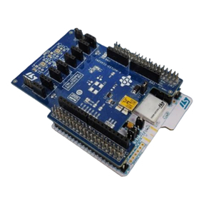
Figure 1. X-NUCLEO-OUT07A1 expansion board
Getting started with the X-NUCLEO-OUT07A1 industrial digital output expansion
board for STM32 Nucleo
UM3285
User manual
UM3285 - Rev 1 - January 2024
For further information contact your local STMicroelectronics sales office. www.st.com

1 Getting started
1.1 Overview
The X-NUCLEO-OUT07A1 embeds the IPS4260LM intelligent power switch (IPS), which features overcurrent and
overtemperature protections for safe output load control, and open load detection. The overcurrent protection
threshold can be configured by a resistor connected between the RILIM pin and the ground: the onboard
connector J8 allows the easy selection of the most typical current limitation levels (0.5A, 1.0A, 2.0A). Also, the
overcurrent protection can be combined with the low dissipative current limitation feature (cutoff) that limits the
time duration of the overload event by a resistor mounted between RCOD and ground. The same connector J8 can
disable the cutoff feature by closing J8[7-8], if necessary (for example, in case of high capacitive loads). The open
load detection can be enabled closing J7 [1-2, 3-4, 5-6, 7-8] or disabled (J7 open).
The board is designed to meet the application requirements for the galvanic isolation between the user and power
interfaces: the isolation is implemented through one monodirectional digital isolator (STISO620 for cumulative
diagnostic signals FAULT and OL), four bidirectional digital isolators (STISO621 for INX driving signals and
related per-channel overload diagnostic) and an isolated DC-DC converter (DC1, generating the 5V and 10V rails
on the process stage from the 5V rail on the logic side).
The expansion board features:
• Based on the IPS4260LM quad low-side switch, which features:
– Operating range from 8 to 50 V
– High Speed operation (trise, tfall < 1us)
– Process stage operating current: configurable from 350 mA (per channel) up to 2A (parallelized
channels)
– Low-power dissipation (RON(TYP) = 260 mΩ)
– Configurable low dissipative cutoff function in overload conditions
– Per-channel overload, short circuit, and thermal junction protections
– Fast decay for inductive loads (VOUT clamp)
– Open load detection
– Undervoltage lock-out
– Loss of ground protection
– HTSSOP20 package
• Galvanic isolation between logic side and process stage by STISO620, STISO621 digital isolators and
isolated DC-DC converter
• Selectable supply of the IPS4260LM from on board isolated DC-DC converter (SW7 close 1-2), or from 24
V supply rail (SW7 close 2-3)
• Process stage operating range: 10 V (SW7 close 1-2) or 10 V to 30 V (SW7 close 2-3)
• Process stage supply rail reverse polarity protections (J1 open)
• Application board logic side operating voltage 3.3 V or 5 V
• Green LEDs for outputs on/off status (J6 close 1-2, 3-4, 5-6, 7-8)
• Open load detection enable (J7 close 1-2, 3-4, 5-6, 7-8)/disable (J7 open)
• Red LEDs for overload and thermal warning (D8) and open load (D6) diagnostic
• Selectable current limitation level (J8[1-2, 3-4, 5-6])
• Cut-Off enable (J8 open 7-8)/disable (J8 close 7-8) options
• Per channel overload diagnostic available on Arduino (CN5[9,10], CN8[5, 6])
• Easy parallelization of input (J9) and output channels (J10)
• Compatible with STM32 Nucleo development boards
• Equipped with Arduino® UNO R3 connectors
• RoHS and China RoHS compliant
• CE certified
UM3285
Getting started
UM3285 - Rev 1 page 2/20
1.1.1 Digital section
The digital section is associated with the STM32 interface and the digital supply voltage to and from the X-
NUCLEO-OUT07A1 expansion board.
Figure 2. X-NUCLEO-OUT07A1 expansion board: digital interface section
The dotted green line indicates the whole digital interface section. The pink rectangles identify the Arduino®
UNOR3 connectors.
The four Arduino® UNO R3 connectors:
• allow the expansion board to communicate with the STM32 Nucleo development board microcontroller
accessing the STM32 peripheral and GPIO resources;
• provide the digital supply voltage between the STM32 Nucleo development board and the X-NUCLEO-
OUT07A1 expansion board, in either direction.
Normally, the STM32 Nucleo development board supplies the expansion board by a 3v3 or 5v0 generated by the
USB. You can select the preferred voltage on the expansion board via SW3 (3v3 closing pins 1-2; 5v0 closing
pins 2-3).
Alternatively, it is possible to supply the STM32 Nucleo development board by the expansion board. In this case,
an external supply voltage (7-12 V) should be connected to the CN4 connector (not mounted by default) on the
expansion board and the ground loop should be closed by mounting D6 (enabling the reverse polarity protection)
or by closing J5 (without reverse polarity).
To supply the VIN voltage rail, it is necessary to:
• close the JP5 jumper between pins 2 and 3 and open the JP1 jumper on the NUCLEO-F401RE;
• open the JP5 jumper between pins 1 and 2 and close the JP5 jumper between pins 3 and 4 on the
NUCLEO-G431RB.
UM3285
Overview
UM3285 - Rev 1 page 3/20

1.1.2 Power section
The X-NUCLEO-OUT07A1 offers four connections points for the loads through the connectors CN2 and CN3. The
other sides of the load are connected to the positive rail of the process stage power supply (usually +24V).
The X-NUCLEO-OUT07A1 offers the user two alternative solutions to supply the IPS4260LM (U1).
With the default solution (J7 closed 1-2), the IPS4260LM is supplied by the onboard isolated DC-DC converter
DC1 that generates the 10V rail supplying the IC. In this case the user just needs to connect the process side
ground of the X-NUCLEO-OUT07A1 (CN1[2]) to the reference voltage of the process stage power supply where
the loads are connected.
With the alternative supply solution (J7 closed 2-3), the IPS4260LM is supplied by the same supply rail where the
load are connected (CN1[1] connected to the 24V rail).
It is important to note that:
• If default supply of IPS4260LM is selected, then the only allowed external fast demagnetization is by D9
(J8 close 1-2). In other words, setting J8 close 2-3 means to enable IPS4260LM internal fast
demagnetization with the EAS limits reported in the datasheet.
• If IPS4260LM is supplied by the process stage power supply, then D9 (J8 close 1-2) or D10 (J8 close 2-3)
can be used. Also, slow demagnetization can be set (J8 close 2-3 and J3 closed).
Figure 3. X-NUCLEO-OUT07A1 expansion board: power section components
1. IPS4260LM
2. Load connectors
3. DC1
4. Power stage ground and 24V rail connector
5. D9
6. D10
7. Output channels status green LEDs
8. FAULT (overload and overtemperature) and OL (open Load) red LEDs
UM3285
Overview
UM3285 - Rev 1 page 4/20

For EMC:
• the SMC30J30CA transient voltage suppressor (U2), enabled by closing J2, is placed between process
stage supply rail and GND tracks to protect the IPS4260LM against surge discharge on the supply rail path
up to ±500 k/2 Ω coupling;
• in the common mode surge testing, two single-layer capacitors (C11 and C12 - not included) must be
soldered at the predisposed locations;
• the IPS4260LM output stages do not require additional EMC protections with respect to the IEC61000-4-2,
IEC61000-4-3, IEC61000-4-4, IEC61000-4-5, IEC61000-4-8 standards
The EMC performances of the X-NUCLEO-OUT07A1 are detailed below:
• for emission, compliance with standards:
– EN IEC 61000-6-3:2021
– EN 55032:2015 +A1:2020
• for immunity, compliance with standards:
– EN IEC 61000-6-1:2019
– EN 55035:2017 +A11:2020
UM3285
Overview
UM3285 - Rev 1 page 5/20

1.2 Hardware requirements
The X-NUCLEO-OUT07A1 expansion board is designed to be used with the NUCLEO-F401RE or NUCLEO-
G431RB STM32 Nucleo development boards.
To function correctly, the X-NUCLEO-OUT07A1 must be plugged onto the matching Arduino® UNO R3 connector
pins on the STM32 Nucleo board as shown below.
Figure 4. X-NUCLEO-OUT07A1 and STM32 Nucleo stack
1.3 System requirements
To use the STM32 Nucleo development boards with the X-NUCLEO-OUT07A1 expansion board, you need:
• a Windows PC/laptop (Windows 7 or above)
• a type A to mini-B USB cable to connect the STM32 Nucleo development board to the PC when using a
NUCLEO-F401RE development board
• a type A to micro-B USB cable to connect the STM32 Nucleo development board to the PC when using a
NUCLEO-G431RB development board
• the X-CUBE-IPS firmware and software package installed on your PC/laptop
UM3285
Hardware requirements
UM3285 - Rev 1 page 6/20

1.4 Board setup
Step 1. Connect the mini-USB or micro-USB cable to your PC to use the X-NUCLEO-OUT07A1 with NUCLEO-
F401RE or NUCLEO-G431RB development board respectively.
Step 2. Download the proper firmware (.bin) onto the STM32 Nucleo development board microcontroller
through STM32ST-LINK utility, STM32CubeProgrammer, and according to your IDE environment, as
detailed in the table below.
Table 1. Nucleo development boards binary files
Nucleo board Binary path
NUCLEO-F401RE Projects\STM32F401RE-
Nucleo\Examples\OUT07A1\FourChannels\Binary\FourChannels.bin
NUCLEO-G431RB Projects\STM32G431RB-Nucleo\Examples\OUT07A1\FourChannels
\Binary\FourChannels.bin
Note: Additional details are available inside the X-CUBE-IPS software package in each example project
folder (Examples\OUT07A1\FourChannels\readme.html)
Step 3. Connect the load on the output connectors (see Section 1.1.2 Power section).
Step 4. Provide the digital supply voltage (see Section 1.1.1 Digital section).
Step 5. Supply the IPS4260LM device (see Section 1.1.2 Power section).
If SW7 = close 1-2, then you just need to connect CN1[2] to the reference (ground) of the same power
supply where the loads are connected.
If SW7 = close 2-3, then connect CN1[1] and CN1[2] to the positive and reference poles of the same
power supply where the loads are connected.
Step 6. Reset the example sequence using the black push button.
Step 7. Push the blue button on the STM32 Nucleo board to choose among the examples provided in the
firmware package.
UM3285
Board setup
UM3285 - Rev 1 page 7/20

2 Schematic diagrams
Figure 5. X-NUCLEO-OUT07A1 circuit schematic (1 of 2)
default open
DEFAULT
PA5
Arduino Connectors
Alternate Nucleo Supply
7V - 12 V
PB3PA4
PA8
PA3
PC7
PA1
PC0
PB10
PC1
PB9
PA10
PB6
Morpho Connectors
(N.M.)
PB4
PB5
PA9
PB0
(7V-12V NUCLEO supply voltage)
PA0
PA7
PA2
PB8
PA6
IOREF
NRST AVDD
DEFAULT
DEFAULT
DEFAULT
Alternate use
DEFAULT
Alternate use
Alternate use
DEFAULT
Alternate use
Alternate use
Alternate use
DEFAULT
DEFAULT
Alternate use
default open
default closed
default:
close 1-2
default:
close 1-2
default:
close 1-2
DEFAULT
DEFAULT
Alternate use
default:
close 1-2
Alternate use
default:
close 1-2
IN4_L
FLT_L
OL_L
IN1_L
IN2_L
IN3_L
DIAG4_L
DIAG1_L
DIAG2_L
DIAG3_L
V_FIELD_RP
OUT1
OUT2
OUT3
OUT4
V_FIELD
3v3 5v0
R119 100 N.M.
SW5
1
2
3
R107 100
R113 100
R101 100
C12
4700pF
J2
R118 100 N.M.
SW6
1
2
3
CN10
SS Q-119-04-L-D
N.M.
1 2
3 4
5 6
7 8
9 10
11 12
13 14
15 16
17 18
19 20
21 22
23 24
25 26
27 28
29 30
31 32
33 34
35 36
37 38
CN6
SS Q-108-04-F-S
1
2
3
4
5
6
7
8
R106 100
CN7
SS Q-119-04-L-D
N.M.
1 2
3 4
5 6
7 8
9 10
11 12
13 14
15 16
17 18
19 20
21 22
23 24
25 26
27 28
29 30
31 32
33 34
35 36
37 38
R112 100
U7
ES DA15P 60-1U1M
N.M
SW4
1
2
3
CN3
1
2
R117 100 N.M.
CN1
1
2
CN2
1
2
R105 100 N.M
C11
4700pF
C10
2.2uF
R111 100
+
C19
47uF (N.M.)
12
R116 100
D5
STPS 1H100A
CN5
SS Q-110-04-F-S
1
2
3
4
5
6
7
8
9
10
R104 100
D6 BAT48 N.M.
U2
SMC30J 30CA
12
R110 100
R115 100
J5
N.M.
TP1
5001
R103 100
R120 100
CN4 N.M.
1
2
R109 100 N.M.
CN8
SS Q-106-04-F-S
1
2
3
4
5
6
R108 100
R114 100
SW2
1
2
3
R102 100
J1
CN9
SS Q-108-04-F-S
1
2
3
4
5
6
7
8SW3
1
2
3
3V3
5V
VIN
VIN
IN4_L
FLT_L
OL_L
IN2_L
IN3_L
DIAG4_L
DIAG1_L
DIAG2_L
DIAG3_L
IN1_L_P C7
IN2_L_P B6
IN4_L
IN2_L_P A9
DIAG1_L_P B8
DIAG2_L
DIAG4_L
DIAG1_L
DIAG3_L
DIAG2_L
DIAG4_L
IN4_L
EARTH
IN3_L_P A0
IN3_L_P A8
IN1_L_P C7
IN1_L_P A5
IN3_L_P A8
IN3_L_P A0
IN1_L
IN2_L_P A9
IN2_L_P B6
OL_L
FLT_L_P B4
DIAG1_L_P B3
DIAG1_L_P B8
DIAG1_L_P B3
FLT_L_P A7
FLT_L_P A7
FLT_L_P B4
IN1_L_P A5
UM3285 - Rev 1 page 8/20
UM3285
Schematic diagrams

Figure 6. X-NUCLEO-OUT07A1 circuit schematic (2 of 2)
default: close 1-2
default =
close 1-2, 3-4,
5-6, 7-8
default =
all open
10V Rail
5V Rail
default =
closed
default =
Close 1-2
default:
close 1-2
default:
close 1-2
default:
open
(Open Load Disabled)
OUT2
OUT3
OUT4
OUT1
FLT_L
OL_L
IN1_L
IN2_L
IN3_L
IN4_L
DIAG1_L
DIAG2_L
DIAG3_L
DIAG4_L
V_FIELD_RP
V_FIELD
5v0
3v3
5v0
C13
100nF
C2 100nF
D2
AC
U8
STISO620
VDD1 1
TXA 2
GND1 4
TXB 3
GND2
5
RXB
6
RXA
7
VDD2
8
D8
RED
AC
J8
con8-2x4-strip-ma le
12
34
56
78
R10
12k
C6 1pF
C1 100nF C14 100nF
R5 5.1k
J6
1 2
3 4
5 6
7 8
U5
STISO621
VDD1
1
RX1
2
GND1
4
TX1
3
GND2 5
RX2 6
TX2 7
VDD2 8
C16 100nF
R23
220k
C5 100nF
SW1
1
2
3
J9
de fault: all ope n
1 2
3 4
5 6
R2
4.7K
D3
AC
R11
12k
R22
220k
J4
C20
4.7uF
R16
22k
C17 100nF
SW7
1
2
3
C21
4.7uF
C18 100nF
R17120K
C8 1pF
D10
SMAJ18CA
12
U4
STISO621
VDD1
1
RX1
2
GND1
4
TX1
3
GND2 5
RX2 6
TX2 7
VDD2 8
J10
de fault: all ope n
1 2
3 4
5 6
R9
12k
R14
22k
R4220k
C7 1pF
C9 1pF
U1 IP S 4260LM
VZ1 3
PGND2 2
PGND1 1
SGND
8
IN3
6
IN4
7
IN1
4
IN2
5
OL
9
FLT
10
EP
21
PGND4 20
LOAD4 14
VZ2 18
LOAD3 15
PGND3 19
VCC 13
LOAD1 17
LOAD2 16
ILIM
12
CoD
11
L1
6.8uH
1 2
C22
4.7uF
R21
220k
R8 5.1k
R1
4.7K
J7
con8-2x4-strip-ma le
1 2
3 4
5 6
7 8
U6
STISO621
VDD1
1
RX1
2
GND1
4
TX1
3
GND2 5
RX2 6
TX2 7
VDD2 8
R12
12k
D1
AC
D7
RED
AC
D4
AC
D9
SMAJ33CA
12
J3
R7 5.1k
C15 100nF
U3
STISO621
VDD1
1
RX1
2
GND1
4
TX1
3
GND2 5
RX2 6
TX2 7
VDD2 8
R6 5.1k
R13
22k
C4 100nF
R15
22k
R20
220k
C3 100nF
R1860k
SW8
1
2
3
R1933k
DC1
PES1-S 5-D5-M
NC
10
GND
1-V0 5
Vin
20V 4
+V0 7
OP EN_LOAD
FAULT
VISO_L
VISO_L
VISO_L
VISO_L
5V_P
5V_P
5V_P
5V_P
VISO_L
FAULT
OP EN_LOAD
5V_P
IN_DIAG1
IN_DIAG2
10V_P
5V_P
IN_DIAG4
VISO_L
IN_DIAG3
IN_DIAG1 IN_DIAG2
IN_DIAG3 IN_DIAG4
IN_DIAG1
IN_DIAG2
IN_DIAG3
IN_DIAG4
OUT4
OUT1
OUT2
OUT3
OUT4
OUT3
OUT2
OUT1
OUT1 OUT2
OUT4OUT3
UM3285 - Rev 1 page 9/20
UM3285
Schematic diagrams

3 Bill of materials
Table 2. X-NUCLEO-OUT07A1 bill of materials
Item Q.ty Ref. Part/Value Description Manufacturer Order code
1 10
C1 C2 C3 C4
C5 C14 C15
C16 C17 C18
100nF, 0603
(1608 Metric),
16V, +/-10%
CAPACITOR
CERAMIC SMD
0603
Wurth
Electronics Inc. 885012206046
2 4 C6 C7 C8 C9 1pF, 0603 (1608
Metric), 50V
CAPACITOR
CERAMIC SMD
0603
Wurth
Electronics Inc. 885012006045
3 0 C19
47uF (N.M.),
Radial, Can,
100V, +/-20%
CAP 47 UF
20% 100 V (not
mounted)
Wurth
Electronics Inc. 860040875002
4 1 C10
2.2uF, 1210
(3225 Metric),
100V, +/-10%
CAP CER
2.2UF 100V
X7R 1210
Wurth
Electronics Inc. 885012209071
5 0 C11 C12
4700pF, 1825
(4564 Metric),
3000V (3kV),
+/-10%
CAP CER
4700PF 3KV
X7R 1825 (not
mounted)
Vishay Vitramon HV1825Y472KXHATHV
6 1 C13
0.1uF, 0805
(2012 Metric),
100V, +/-10%
CAP CER
0.1UF 100V
X7R 0805
Wurth
Electronics Inc. 885012207128
7 3 C20, C21, C22
4.7u, F 0805
(2012 Metric),
10V, +/-10%
CAP CER
4.7UF 10V X7R
0805
Wurth
Electronics Inc. 885012207025
8 1 L1 6.8uH, 0.18A,
+/-10%
INDUCTOR,
6.8UH, 10%,
0.18A, 43MHZ
Wurth
Electronics Inc. 74476406
9 1 DC1
PES1-S5-D5-M,
10-SMD
Module, 6
Leads, 1W
DC DC
CONVERTER
+/-5V 1W
CUI Inc. PES1-S5-D5-M-TR
10 3 CN1 CN2 CN3 691214110002,
7.4X7 pitch 3.5
TERM BLK
2POS SIDE
ENT 3.5MM
PCB
Wurth
Electronics Inc. 691214110002
11 0 CN4 691214110002,
7.4X7 pitch 3.5
TERM BLK
2POS SIDE
ENT 3.5MM
PCB (not
mounted)
Wurth
Electronics Inc. 691214110002
12 1 CN5 SSQ-110-04-F-
S
CONN RCPT
10POS 0.1
GOLD PCB
Samtec Inc. SSQ-110-04-F-S
13 2 CN6 CN9 SSQ-108-04-F-
S
CONN RCPT
8POS 0.1
GOLD PCB
Samtec Inc. SSQ-108-04-F-S
14 0 CN7 CN10 SSQ-119-04-L-
D
CONN RCPT
38POS 0.1
GOLD PCB (not
mounted)
Samtec Inc. SSQ-119-04-L-D
15 1 CN8 SSQ-106-04-F-
S
CONN RCPT
6POS 0.1
GOLD PCB
Samtec Inc. SSQ-106-04-F-S
UM3285
Bill of materials
UM3285 - Rev 1 page 10/20

Item Q.ty Ref. Part/Value Description Manufacturer Order code
16 1 D5
STPS1H100A,
DO-214AC,
SMA, 1A
DIODE
SCHOTTKY
100V 1A SMA
ST STPS1H100A
17 0 D6
BAT48JFILM,
SC-76,
SOD-323,
750mV @
200mA 350mA
(DC)
DIODE
SCHOTTKY
40V 350MA
SOD323 (not
mounted)
ST BAT48JFILM
18 4 D1 D2 D3 D4
150060VS7500
0, 0603 (1608
Metric), 20mA
LED GREEN
CLEAR 0603
SMD
Wurth
Electronics Inc. 150060VS75000
19 2 D7 D8
150060RS7500
0, 0603 (1608
Metric), 20mA
LED RED
CLEAR 0603
SMD
Wurth
Electronics Inc. 150060RS75000
20 4 J1 J2 J3 J4 JUMPER-con2-
strip-male
JUMPER-
CONN
HEADER .100
STR 2POS
Wurth
Electronics Inc. 61300211121
21 0 J5 JUMPER-con2-
strip-male
JUMPER-
CONN
HEADER .100
STR 2POS (not
mounted)
Wurth
Electronics Inc. 61300211121
22 3 J6 J7 J8 con8-2x4-strip-
male
CONN
HEADER .100
DUAL STR
8POS
Wurth
Electronics Inc. 61300821121
23 2 J9 J10 con6-2x3-strip-
male
CONN
HEADER .100
DUAL STR
6POS
Wurth
Electronics Inc. 61300621121
24 2 R1 R2
4.7k, 0603
(1608 Metric),
0.1W, 1/10W,
+/-1%
RES SMD 4.7K
OHM 1% 1/10W
0603
ANY ANY
25 5 R4 R20 R21
R22 R23
220k 0603
(1608 Metric)
0.1W, 1/10W
1%
CHIP
RESISTOR
SMD 1% 1/10W
0603
ANY ANY
26 4 R5 R6 R7 R8
5.1k 0603 (1608
Metric) 0.1W,
1/10W 1%
RES SMD 5.1K
OHM 1% 1/10W
0603
ANY ANY
27 4 R9 R10 R11
R12
12k 0603 (1608
Metric) 0.1W,
1/10W 1%
RES SMD 12K
OHM 1% 1/10W
0603
ANY ANY
28 4 R13 R14 R15
R16
22k 0603 (1608
Metric) 0.1W,
1/10W 1%
RES SMD 22K
OHM 1% 1/10W
0603
ANY ANY
29 1 R17
120k 0603
(1608 Metric)
0.1W, 1/10W
1%
RES SMD 120K
OHM 1% 1/10W
0603
ANY ANY
30 1 R18
60k 0603 (1608
Metric) 0.1W,
1/10W 1%
RES SMD 60K
OHM 1% 1/10W
0603
ANY ANY
UM3285
Bill of materials
UM3285 - Rev 1 page 11/20

Item Q.ty Ref. Part/Value Description Manufacturer Order code
31 1 R19
33k 0603 (1608
Metric) 0.1W,
1/10W 1%
RES SMD 33K
OHM 1% 1/10W
0603
ANY ANY
32 15
R101 R102
R103 R104
R106 R107
R108 R110
R111 R112
R113 R114
R115 R116
R120
100, 0603 (1608
Metric), 0.1W,
1/10W, +/-1%
RES SMD 100
OHM 1% 1/10W
0603
ANY ANY
33 0
R105 R109
R117 R118
R119
100 0603 (1608
Metric) 0.1W,
1/10W 1%
RES SMD 100
OHM 1% 1/10W
0603 (not
mounted)
ANY ANY
34 8
SW1 SW2 SW3
SW4 SW5 SW6
SW7 SW8
con3-strip-male
CONN
HEADER VERT
3POS 2.54MM
MALE
Würth
Elektronik 61300311121
35 1 TP1
5001 0.100" Dia
x 0.180" L
(2.54mm x
4.57mm)
TEST POINT
PC MINI .040"D
BLACK
Keystone
Electronics 5001
36 1 U1
IPS4260LM
IPS4260L, 20-
TSSOP (0.173",
4.40mm Width)
QUAD LOW-
SIDE
INTELLIGENT
POWER
ST IPS4260LM, IPS4260L
37 1 U2 SMC30J30CA,
SMC, 3kW
TVS DIODE
33.3V 48.4V
SMC
ST SMC30J30CA
38 4 U3 U4 U5 U6
STISO621, 8-
SOIC (0.268",
6.81mm Width)
Dual Channel
Digital Isolator ST STISO621
39 1 U8
STISO620, 8-
SOIC (0.268",
6.81mm Width)
Dual Channel
Digital Isolator ST STISO620
40 0 U7 ESDA15P60-1U
1M, 2-UDFN
TVS DIODE
13.2V 22.7V
1610 (not
mounted)
ST ESDA15P60-1U1M
41 1 D9
SMAJ33CA,
SMA (Jedec
DO214-AC)
TVS DIODE
36.7V 53.3V ST SMAJ33CA
42 1 D10
SMAJ18CA,
SMA (Jedec
DO214-AC)
TVS DIODE
20.0V 29.2V ST SMAJ18CA
43 27 N/A Shunt, 2.54mm Close jumper Wurth
Electronics Inc. 60900213421
UM3285
Bill of materials
UM3285 - Rev 1 page 12/20
4 Board versions
Table 3. X-NUCLEO-OUT07A1 versions
PCB version Schematic diagrams Bill of materials
X$NUCLEO-OUT07A1 (1) X$NUCLEO-OUT07A1 schematic diagrams X$NUCLEO-OUT07A1 bill of materials
1. This code identifies the X-NUCLEO-OUT07A1 evaluation board first version. It is printed on the board PCB.
UM3285
Board versions
UM3285 - Rev 1 page 13/20

5 Regulatory compliance information
Notice for US Federal Communication Commission (FCC)
For evaluation only; not FCC approved for resale
FCC NOTICE - This kit is designed to allow:
(1) Product developers to evaluate electronic components, circuitry, or software associated with the kit to
determine
whether to incorporate such items in a finished product and
(2) Software developers to write software applications for use with the end product.
This kit is not a finished product and when assembled may not be resold or otherwise marketed unless all
required FCC equipment authorizations are first obtained. Operation is subject to the condition that this product
not cause harmful interference to licensed radio stations and that this product accept harmful interference. Unless
the assembled kit is designed to operate under part 15, part 18 or part 95 of this chapter, the operator of the kit
must operate under the authority of an FCC license holder or must secure an experimental authorization under
part 5 of this chapter 3.1.2.
Notice for Innovation, Science and Economic Development Canada (ISED)
For evaluation purposes only. This kit generates, uses, and can radiate radio frequency energy and has not been
tested for compliance with the limits of computing devices pursuant to Industry Canada (IC) rules.
À des fins d'évaluation uniquement. Ce kit génère, utilise et peut émettre de l'énergie radiofréquence et n'a pas
été testé pour sa conformité aux limites des appareils informatiques conformément aux règles d'Industrie Canada
(IC).
Notice for the European Union
This device is in conformity with the essential requirements of the Directive 2014/30/EU (EMC) and of the
Directive 2015/863/EU (RoHS).
Notice for the United Kingdom
This device is in compliance with the UK Electromagnetic Compatibility Regulations 2016 (UK S.I. 2016 No. 1091)
and with the Restriction of the Use of Certain Hazardous Substances in Electrical and Electronic Equipment
Regulations 2012 (UK S.I. 2012 No. 3032).
UM3285
Regulatory compliance information
UM3285 - Rev 1 page 14/20

Revision history
Table 4. Document revision history
Date Revision Changes
25-Jan-2024 1 Initial release.
UM3285
UM3285 - Rev 1 page 16/20

Contents
1Getting started ....................................................................2
1.1 Overview .....................................................................2
1.1.1 Digital section ...........................................................3
1.1.2 Power section ...........................................................4
1.2 Hardware requirements .........................................................6
1.3 System requirements ...........................................................6
1.4 Board setup ...................................................................7
2Schematic diagrams ...............................................................8
3Bill of materials...................................................................10
4Board versions ...................................................................13
5Regulatory compliance information ...............................................14
6References .......................................................................15
Revision history .......................................................................16
List of tables ..........................................................................18
List of figures..........................................................................19
UM3285
Contents
UM3285 - Rev 1 page 17/20

List of tables
Table 1. Nucleo development boards binary files ....................................................7
Table 2. X-NUCLEO-OUT07A1 bill of materials .................................................... 10
Table 3. X-NUCLEO-OUT07A1 versions .........................................................13
Table 4. Document revision history .............................................................16
UM3285
List of tables
UM3285 - Rev 1 page 18/20

List of figures
Figure 1. X-NUCLEO-OUT07A1 expansion board...................................................1
Figure 2. X-NUCLEO-OUT07A1 expansion board: digital interface section .................................3
Figure 3. X-NUCLEO-OUT07A1 expansion board: power section components ...............................4
Figure 4. X-NUCLEO-OUT07A1 and STM32 Nucleo stack.............................................6
Figure 5. X-NUCLEO-OUT07A1 circuit schematic (1 of 2) .............................................8
Figure 6. X-NUCLEO-OUT07A1 circuit schematic (2 of 2) .............................................9
UM3285
List of figures
UM3285 - Rev 1 page 19/20

IMPORTANT NOTICE – READ CAREFULLY
STMicroelectronics NV and its subsidiaries (“ST”) reserve the right to make changes, corrections, enhancements, modifications, and improvements to ST
products and/or to this document at any time without notice. Purchasers should obtain the latest relevant information on ST products before placing orders. ST
products are sold pursuant to ST’s terms and conditions of sale in place at the time of order acknowledgment.
Purchasers are solely responsible for the choice, selection, and use of ST products and ST assumes no liability for application assistance or the design of
purchasers’ products.
No license, express or implied, to any intellectual property right is granted by ST herein.
Resale of ST products with provisions different from the information set forth herein shall void any warranty granted by ST for such product.
ST and the ST logo are trademarks of ST. For additional information about ST trademarks, refer to www.st.com/trademarks. All other product or service names
are the property of their respective owners.
Information in this document supersedes and replaces information previously supplied in any prior versions of this document.
© 2024 STMicroelectronics – All rights reserved
UM3285
UM3285 - Rev 1 page 20/20
Table of contents
Other ST Computer Hardware manuals

ST
ST STSW-L9961BMS User manual

ST
ST STM32Cube User manual

ST
ST X-NUCLEO-53L7A1 User manual

ST
ST X-NUCLEO-GNSS2A1 User manual

ST
ST X-NUCLEO-GFX01M1 User manual

ST
ST X-NUCLEO-IDW04A1 User manual

ST
ST X-NUCLEO-IDB04A1 User manual

ST
ST ControlBD-7FMC2 User manual

ST
ST STEVAL-IDB013V1 Administrator Guide

ST
ST UM1472 User manual

ST
ST STM32 Nucleo User manual

ST
ST FP-SNS-FLIGHT1 User manual

ST
ST STM32U5G9J-DK2 User manual

ST
ST STM32G0 User manual

ST
ST STM32 Nucleo User manual

ST
ST STEVAL-STWINMA2 User manual

ST
ST STM32U5 Nucleo-64 User manual

ST
ST STLINK-V3PWR User manual

ST
ST STEVAL-IFP047V1 User manual

ST
ST AEK-COM-ISOSPI1 User manual