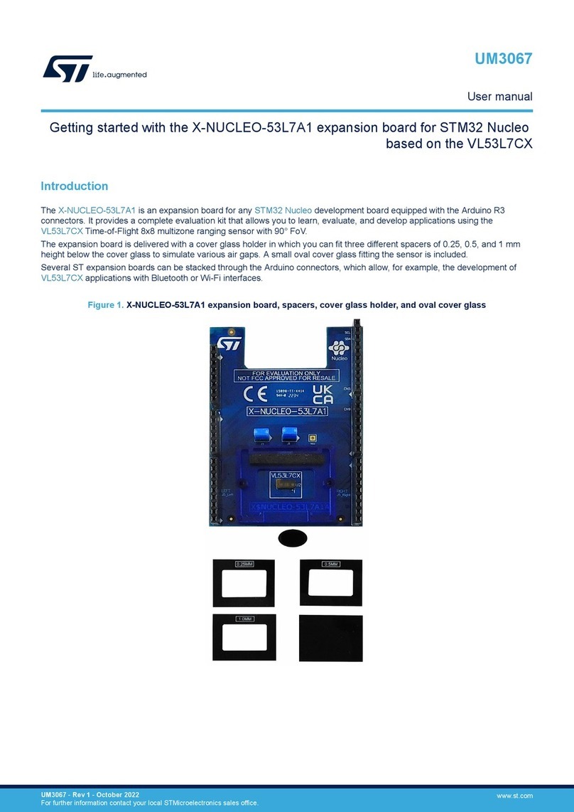
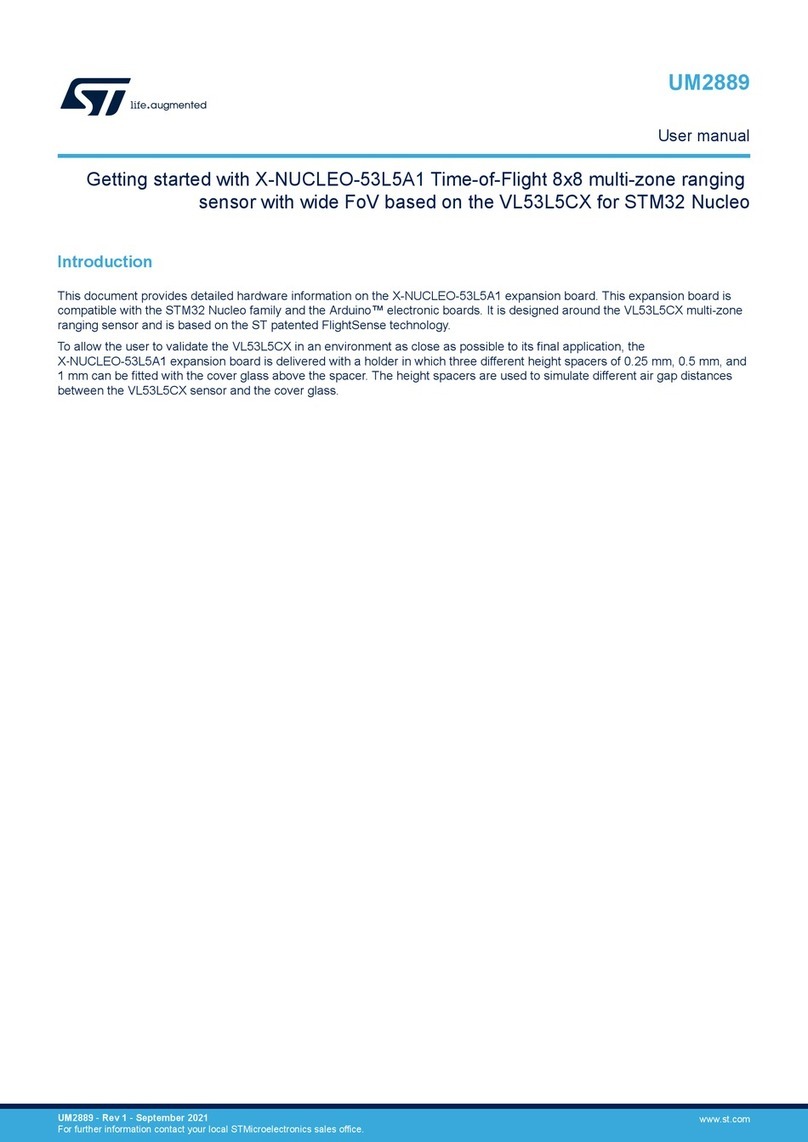
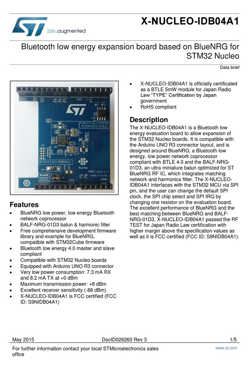
ST STLINK-V3PWR User manual

Introduction
STLINK-V3PWR is a two-in-one standalone debugger probe and a source measurement unit (SMU) designed to synchronize
code execution with a power consumption of STM32 applications in real time. This tool is specifically adapted for power
consumption optimization (patent pending).
STLINK-V3PWR can be used as a standalone source measurement unit to supply power and measure the current consumption
of the target application. The product keeps the output voltage constant during fast current transient from very low current to
high current.
STLINK-V3PWR is also a standalone debugging and programming probe for STM32 microcontrollers. The product embeds a
multi-path bridge interface with an integrated level shifter to adapt to the target application I/Os voltage.
STLINK-V3PWR USB Type-C® connector allows data communication with the host PC and sinks up to 5 V/3 A to supply both
the probe and the target application, via the SMU and the auxiliary output.
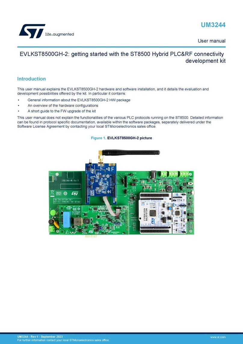
Figure 1. STLINK-V3PWR top, bottom, and cable views
Picture is not contractual.
Source measurement unit (SMU) and debugger/programmer for
STM32 microcontrollers
UM3097
User manual
UM3097 - Rev 1 - March 2023
For further information contact your local STMicroelectronics sales office. www.st.com

1Features
• 1‑Quadrant source measurement unit with high resolution, and measurement flexibility:
–Programmable voltage source from 1.6 to 3.6 V
– Output current rating 500 mA with overcurrent protection (OCP) at 550 mA
– Programmable sampling rate from 1 SPS to 100 kSPS
– Dynamic measurement:
◦ 100 nA to 500 mA current / 160 nW to 1.65 W power measurements
◦ 50 kHz bandwidth / 1.6 MHz acquisition / 2% accuracy
◦ Compatible with EEMBC® ULPMark™ tests
• Auxiliary output voltage source from 1.6 to 3.6 V under up to 2 A (no current measurement, OCP at 2.5 A)
• Debugging of embedded applications:
– JTAG / Serial Wire Debug (SWD):
◦ SWD (Serial Wire Debug) and SWV (Serial Wire Viewer) communication support up to 10 MHz
◦ JTAG communication support up to 20 MHz
– UART interface on Virtual COM port (VCP) with frequency up to 12 MHz
– Multi-path bridge USB to SPI/I2C/CAN/GPIOs
– Integrated level shifter I/O voltage 1.6 to 3.6V adaptable
• Four bi-color LEDs providing probe state
• Three STDC14 to MIPI10 / STDC14 / MIPI20 flat cables with 1.27 mm pitch connectors
• Four cables (two male/male and two male/female)
• USB Type-C® connector:
– Powered through USB Type-C® (5 V/1.5 A minimum)
– USB 2.0 high‑speed interface
– Probe firmware update through USB
• Direct support from STM32CubeMonitor-Power software tool
UM3097
Features
UM3097 - Rev 1 page 2/30

2Ordering information
To order the STLINK-V3PWR SMU and in-circuit debugger/programmer for STM32, refer to Table 1.
Table 1. Ordering information
Order code Reference Description
STLINK-V3PWR STLINK-V3PWR Debug board for STM32 microcontrollers including
simultaneous current measurement
UM3097
Ordering information
UM3097 - Rev 1 page 3/30

3Development environment
STLINK-V3PWR runs with an STM32 32‑bit microcontroller based on the Arm® Cortex®-M core.
Note: Arm is a registered trademark of Arm Limited (or its subsidiaries) in the US and/or elsewhere.
3.1 System requirements
• Multi‑OS support: Windows® 10 or beyond, Linux® 64-bit, or macOS®
•USB Type-A or USB Type-C® to USB Type-C® cable
Note: macOS® is a trademark of Apple Inc., registered in the U.S. and other countries and regions.
Linux® is a registered trademark of Linus Torvalds.
Windows is a trademark of the Microsoft group of companies.
3.2 Development toolchains
• IAR Systems® - IAR Embedded Workbench®(1)
• Keil® - MDK-ARM(1)
• STMicroelectronics - STM32CubeIDE
1. On Windows® only.
3.3 Toolchain versions
Table 2. Glossary
Toolchain Description Minimum version
STM32CubeProgrammer ST programming tool for ST microcontrollers 1.12.0
IAR Systems® EWARM Third-party debugger for STM32 including current
measurement support 9.32.2
Keil® MDK‑ARM Third-party debugger for STM32 including current
measurement support 5.38
STM32CubeMonitor-Power ST monitoring tool for power consumption 1.2.0
STM32CubeIDE ST debugger for STM32 1.12.0
STLINK-V3-BRIDGE ST software package: C++ API compatible with the bridge
interface of STLINK-V3 and STLINK-V3PWR 1.1.0
3.4 Drivers and firmware upgrade
The driver installation is not mandatory since Windows® 10 but allocates an ST‑specific name to the ST-LINK
COM port in the system device manager. For details information regarding the ST-LINK USB driver, refer to the
technical note Overview of ST-LINK derivatives (TN1235).
STLINK-V3PWR embeds a firmware upgrade (stsw-link007) mechanism through the USB port. As the firmware
might evolve during the lifetime of the STLINK-V3PWR product, to add new functionalities, fix bugs, and support
new microcontroller families, it is recommended to visit the www.st.com website before starting to use STLINK-
V3PWR and periodically, to stay up to date with the latest firmware version. For details information about firmware
upgrades, refer to the technical note Overview of ST-LINK derivatives (TN1235).
UM3097
Development environment
UM3097 - Rev 1 page 4/30

4Glossary
Table 3. Glossary
Term Meaning
AUX Auxiliary output voltage
Target application Target product application embedding an STM32 MCU with peripherals
GND Ground
OCP Over current protection
OUT Main output voltage
OVP Over voltage protection
SMPS Switched‑mode power supply
SMU Source measure unit
UM3097
Glossary
UM3097 - Rev 1 page 5/30

5Product information
5.1 Product content
The STLINK-V3PWR kit contains:
•STLINK-V3PWR probe
• Four wires:
– Two wires male/male (red and black)
– Two wire male/female (red and black)
• Three debug cables allowing the connection from the STDC14 (DEBUG port) to:
– STDC14 connector (1.27 mm pitch) Samtec FFSD-07-D-05.90-01-N
– MIPI10/ARM10-compatible connector (1.27 mm pitch) Samtec FFSD-05/07-D-05.90-01-N
– MIPI20/ARM20-compatible connector (1.27 mm pitch) Samtec FFSD-10/07-D-05.90-01-N
Note: To support the JTAG interface, in 2.54 mm pitch, use a dedicated dongle MIPI/ARM20 to JTAG (2.54 mm) (for
example: dongle “JTAG 20 Pin 2.54 mm to 10 Pin 1.27 mm adapter”)
5.2 STLINK-V3PWR connectors and LEDs identification
This section aims to identify the location of the STLINK-V3PWR connectors and LEDs.
They are illustrated with the silkscreen on the casing serving as a functional reference for most connectors. A
connection overview is given here:
•USB-C: USB Type-C® receptacle for host PC connection using a USB Type-C® to USB Type-C® cable for
the STLINK-V3PWR power supply and data transfer. Refer to Section 5.3 USB connection with a host PC.
•DEBUG: STDC14 2x7-pin male connector with 1.27 mm pitch for connection to an STM32 target
application for debugging operations. Three different flat cables are included in the packaging to connect
with standard connectors MIPI10/ARM 10, STDC14, and ARM 20. Refer to Section 9.3 DEBUG (STM32
JTAG/SWD and VCP).
•BRIDGE: 2x11-pin male connector with 2.54 mm pitch for connection to an STM32 target application for
data communication (typically STM32’s bootloader) with several common interfaces via a proprietary USB
interface. Refer to Section 9.4 BRIDGE (I2C, CAN, SPI, UART, and GPIO).
•POWER: 3-pin screw connector with a 5 mm pitch allows supplying the target application via two
independent programmable power source: OUT (refer to Section 7.2 SMU output (OUT)) and AUX (refer
to Section 7.3 Auxiliary power source output (AUX)).
•LEDs: 4x3-colors LED to indicate the state of the product. Refer to Section 7.6 LEDs management.
UM3097
Product information
UM3097 - Rev 1 page 6/30

Figure 2. STLINK-V3PWR connections
DT59112V1
DEBUG
POWER
BRIDGE
LEDs
USB-C
Note: USB-C, DEBUG, BRIDGE, POWER connectors, and LED terminologies used in this document are referring to
the naming defined in Figure 2.
5.3 USB connection with a host PC
5.3.1 Pre‑requisite
The STLINK-V3PWR’s USB-C must be connected to a USB Type-A host PC or hub port supporting charging
(having a “spark” logo) or to a USB Type-C® host PC or hub port. Refer to Table 4 for details.
The USB LED indicates if STLINK-V3PWR is connected to a USB port supporting charging:
• USB LED in green color: The USB host port supports charging and the STLINK-V3PWR SMU (OUT) and
auxiliary output (AUX) are enabled.
• USB LED in orange color: The USB host port does not support charging and the STLINK-V3PWR SMU
(OUT) and auxiliary output (AUX) are disabled.
Note: The debugger and bridges interfaces are always functional even if the STLINK-V3PWR’s USB-C is connected
onto a standard USB HS (high
‑
speed) host port.
5.3.2 Detailed description
For the data interface, the STLINK-V3PWR’s USB-C must be connected to a USB HS host port. USB FS (full
speed) or USB LS (low speed) modes are not supported. Connecting STLINK-V3PWR to a USB SS (super
speed) host port is also possible as the USB SS port runs in HS mode.
For the power, the STLINK-V3PWR internal circuitry, including the SMU output (OUT), and the auxiliary output
(AUX) are powered by USB-C. Accordingly, the host PC must be capable to supply them, especially for the SMU
output (OUT) and the auxiliary output (AUX) that can require a significant peak of energy to power supply a
complete target application.
STLINK-V3PWR automatically detects the power budget advertised by the host PC USB port. As mentioned in
Section 5.3.1, the STLINK-V3PWR’s USB-C must be connected to a USB host PC or USB hub port that can
provide 5 V/1.5 A minimum, typically a USB host port supporting charging. Refer to Table 4 for details.
UM3097
USB connection with a host PC
UM3097 - Rev 1 page 7/30

Table 4. USB host PC or hub port identification
USB host port Port identification STLINK-V3PWR compatibility USB LED
color
Standard USB Type-A port (500 mA) OUT and AUX disabled orange
Charging USB Type-A port (1.5 A) OK green
USB Type-C®(1) port (1.5 or 3 A) OK green
Charging USB Type-C® port (3 A) OK green
1. Some USB Type-C® ports without the “spark” logo might be advertised as 500 mA ports. In that case, STLINK-V3PWR
works with the OUT and AUX disabled and the USB LED lights in orange color.
Note: Connection to a USB charger is not a functional use case for STLINK-V3PWR. In that case, USB LED lights
in green color (valid power source) and COM LED blinks red color (waiting for USB enumeration). Refer to
Section 7.6 LEDs management.
5.4 Mechanical information
Figure 3. Product dimensions
DT59117V1
90 mm
20 mm
70 mm
5.5 Thermal recommendation
STLINK-V3PWR is recommended to operate at the temperature range specified in Table 11.
STLINK-V3PWR uses precision components that are affected by temperature changes. It is recommended to use
it at a place where the thermal gradient or airflow is minimum. A typical laboratory bench or table might be an
optimal location.
Accordingly, airflow cooling holes on the top and the bottom of STLINK-V3PWR must be kept free to ease air
cooling.
Hence it is recommended to start the measurement after waiting for a few minutes after the product is plugged
into the USB port and a connection is established. This ensures the entire product self‑heating to reach
thermal equilibrium and avoid triggering a self‑calibration sequence during measurement acquisition (refer to
Section 7.2.3 Self‑calibration management).
5.6 Known limitation
The STLINK-V3PWR internal acquisition circuitry is sensitive to vibration and shock. If vibration or shock occurs
during acquisition, STLINK-V3PWR sends acquisition data containing erroneous peak current.
UM3097
Mechanical information
UM3097 - Rev 1 page 8/30

6Quick start
This section describes how to start with STLINK-V3PWR to make power measurements:
1. Check that the bundle is complete (STLINK-V3PWR with three flat cables and a bundle of four wire
jumpers).
2. Install or update the power measurement software (for example STM32CubeMonitor-Power).
3. Connect a USB Type-C® to USB Type-C® cable (recommended) or USB Type-A to USB Type-C® cable
between STLINK-V3PWR and the PC (refer to Section 5.3 USB connection with a host PC).
4. Check the LED status:
– The USB LED must turn green: STLINK-V3PWR is supplied by a valid power source from PC.
– The COM LED must turn red: STLINK-V3PWR debugger is ready.
5. Hardware configuration for power measurement: Connect the STLINK-V3PWR’s SMU (OUT and GND)
onto the power supply input of the target application using wire jumpers. Refer to Section 6.1 Typical
application.
6. Software configuration for power measurement: Refer to Section 6.2 Software configuration.
6.1 Typical application
6.1.1 Connection with a target application for power measurements
STLINK-V3PWR provides two voltage‑regulated power sources: OUT and AUX:
•OUT is a programmable voltage‑regulated power source including current measurement: Refer to
Section 7.2 SMU output (OUT).
• AUX is a programmable voltage‑regulated power source only: Refer to Section 7.3 Auxiliary power source
output (AUX).
Figure 4 provides a basic connection example of STLINK-V3PWR with a target application.
Figure 4. STLINK-V3PWR connection
DT59118V1
VDD
Peripherals
Target
application
optional
+3V3 VDD
3V3_PERIPH
DEBUG
debug I/F
ctrl I/F
GND
• Connect OUT to the target application power supply input to be measured (for example pin +3V3 of an
STM32 Nucleo board) using a wire jumper provided in the kit.
•Connect the GND to the target application ground (for example pin GND of an STM32 Nucleo board) using
a wire jumper provided in the kit.
• (Optional) Connect the AUX power source to the target application input power supply that does not require
to be measured.
6.1.2 Recommendations for power measurements
The use of wire jumpers provided in the kit must be limited to target applications not consuming more than
100 mA to avoid voltage drop through wire jumper cables.
UM3097
Quick start
UM3097 - Rev 1 page 9/30

For target applications having significant current consumption, it is recommended to use cables with adapted
conductor diameter to limit voltage drop through the cable due to wire resistance and current consumption of the
target application.
In addition, it is recommended to not use wires longer than ~30 cm and twist them (OUT and GND wires) to
reduce parasitic inductance.
6.2 Software configuration
1. Launch the STM32CubeMonitor-Power application.
2. Select the COM port of the device.
Figure 5. STM32CubeMonitor-Power setting
3. Click on the "TAKE CONTROL" button to handle the STLINK-V3PWR probe.
– ACQUISITION & REPLAY:
– Set "Sampling Frequency" to 20000 Hz [recommended value]
– Set "Acquisition Time" to 10 s
– Set "Current Threshold" to 1000 µA
– Set "Trigger Source" to "sw" (software)
– Set "Trigger Delay" to 1ms
– Set the desired "Input Voltage" of the target application inside the range 1600 mV/3600 mV
4. Click on the "START ACQUISITION" button
5. The STLINK-V3PWR's SMU turns on and current measurement acquisition starts:
– OUT and AUX LEDs turn on green (output voltage turned on)
– Current measurement is displayed in real time in the STM32CubeMonitor-Power main window.
Note: Refer to the user manual STM32CubeMonitor-Power software tool for power and ultra-low-power
measurements (UM2202).
UM3097
Software configuration
UM3097 - Rev 1 page 10/30

7STLINK-V3PWR functional description
7.1 STLINK-V3PWR overview
The following sections provide a functional description of the STLINK-V3PWR features.
Figure 6 provides a high-level block diagram of the STLINK-V3PWR internal circuitry that illustrates a typical
connection of STLINK-V3PWR with a host PC and with a target application.
Figure 6. STLINK-V3PWR block diagram
DT59120V1
SMU
USB Type C®
DEBUG
POWER
AUX
OUT
Bridge
USB
COM
OUT
AUX
STLINK-V3PWR Target
DEBUG
STPMIC1
Level shifter
Level
shifter
Peripherals
STM32H745
VDD
7.2 SMU output (OUT)
The STLINK-V3PWR’s SMU output is accessible on the POWER’s 3‑pin screw connector between the OUT pin
(positive node) and GND pin (negative node). Figure 7 provides a block diagram of the SMU.
Figure 7. STLINK-V3PWR SMU block diagram
DT59121V1
OUT
VSOURCE
A
Imeter
V
Feedback to
regulate VOUT
IOUT
Target
application
GND
VOUT
SMU
UM3097
STLINK-V3PWR functional description
UM3097 - Rev 1 page 11/30

The STLINK-V3PWR’s SMU operates as a 1‑quadrant voltage source and current meter. The SMU operating
area is illustrated in Figure 8.
Figure 8. STLINK-V3PWR SMU operating area
DT59122V1
+1.6 V +3.6 V
+500 mA
operating
measurement
area
0
IOUT
VOUT
OCPTH
overcurrent
OCPMAX
short-circuit
7.2.1 Voltage source
The SMU output voltage is programmable from +1.6 to +3.6 V by 100 mV step.
The SMU output voltage keeps stable and accurate over the operating measurement area (refer to Figure 8),
even with a large capacitive load (order of 100 µF) that usually causes SMU oscillating.
It has excellent load transient response, even for a transient starting from very low current to high current with
fast current rise time (refer to VOUT_LO in Table 12). This is especially suitable to supply an STM32 microcontroller
operating from STANDBY mode (very low current) to RUN mode (high current) without impacting its power supply
voltage.
The SMU can source a 500 mA continuous output current.
Above 500 mA and up to OCPTH (550 mA) output current, the SMU output starts entering self-protection mode.
Output voltage decreases slowly as output current increases.
It can safely tolerate overcurrent and short circuits (refer to Section 7.2.4 Overcurrent and short circuit
management).
Voltage source power ON/ power OFF management
• The voltage source is OFF after STLINK-V3PWR powers up (USB cable insertion).
• The default output voltage is 3.3 V. Any voltage change must be performed before turning on the voltage
source.
• By default, the voltage source is automatically turned ON when a current measurement acquisition is
started.
• By default, the voltage source stays ON after a current measurement acquisition ends or stops.
7.2.2 Current measurement
The STLINK-V3PWR SMU is composed of four analog current measurement paths having 50 kHz analog
bandwidth. Current sample acquisitions of the four measurement paths are performed by an STM32H745 using
two 12‑bit ADCs working in parallel, each at a 1.6 MHz sampling frequency. The embedded post‑processing
algorithms aim to manage current range selection and to perform noise reduction. SMU provides a sampling rate
of up to 100 kSPS (kilosamples per second) and down to 1 SPS to the host PC via a USB interface.
UM3097
SMU output (OUT)
UM3097 - Rev 1 page 12/30

The four measurement paths have a fixed current range (refer to Figure 9). Range selections are fully automated
at run time by post‑processing algorithms allowing a continuous current acquisition from a few nA to 500 mA.
Figure 9. SMU current measurement ranges
DT59123V1
10-9
1nA
Iout (A)
(load)
10-8 10-7 10-6
1 µA
10-5 10-4 10-3
1 mA
10-2 10-1 1
1 A
res: 1.5 nA
5 µA
RANGE1
380 µA
RANGE2
RANGE3
15 mA 500 mA
RANGE4
res: 5 nA
res: 60 nA res: 1 µA
res: 5 µA res: 15 µA
res: 150 µA res: 250 µA
Impact of noise on sampling rate selection
The sampling rate selection has significant impacts on measurements.
Using the maximum sampling rate allows the user to catch fast current transient activities but it intrinsically
increases the noise level making small current variations hidden in the noise level.
Reciprocally, using the minimum sampling rate allows the user to measure small current variations and average
the noise but it smooths fast current transient activities.
Note: Sampling rate selection does not impact the current measurement DC accuracy.
7.2.3 Self‑calibration management
STLINK-V3PWR has built‑in self‑calibration circuitry to compensate for the current measurements offset due to
temperature variation.
A self-calibration is automatically performed during current measurements acquisition every +/- 5°C temperature
change inside STLINK-V3PWR.
During the self-calibration sequence, STLINK-V3PWR keeps the SMU output voltage (OUT) enabled but STLINK-
V3PWR stops sending measurement data to the host PC. Once the self‑calibration sequence ends, STLINK-
V3PWR restarts sending measurement data to the host PC.
A self‑calibration sequence duration is approximately 15 ms and does not require user intervention.
Each time a self-calibration occurs:
• A popup is displayed on the STM32CubeMonitor-Power windows to inform the user that acquisition data is
stopped for self-calibration sequence duration.
• The OUT LED turns in orange color (refer to Table 8. OUT LED).
7.2.4 Overcurrent and short circuit management
The SMU output is protected against overcurrent higher than OCPTH (refer to Table 12) and short circuits.
It can safely tolerate short overcurrent or peak current before triggering an OCP (overcurrent protection). This is
suitable to keep the target application operating without crashing during peak transient activities where current
consumption is higher than OCPTH.
When OCPTH < IOUT < OCPMAX, the output voltage decreases as the output current increases:
VOUT ≈ VOUTnom – 0.3 x IOUT
Short overcurrent
A short overcurrent is a current consumption within OCPTH < IOUT < OCPMAX having a duration less than
t_short_ocp (refer to Table 12).
Nevertheless, the SMU returns erroneous current measurement values to the host PC as the current consumption
is above the operating measurement area.
UM3097
SMU output (OUT)
UM3097 - Rev 1 page 13/30

If the overcurrent disappears before t_short_ocp duration, then the OUT LED blinks red/green for 2s duration (refer
to Table 8. OUT LED) and a warning popup message is displayed on the STM32CubeMonitor-Power windows.
An overcurrent longer than t_short_ocp duration is considered a long overcurrent.
Long overcurrent
A long overcurrent is a current consumption within OCPth < IOUT < OCPmax having a duration longer than
t_short_ocp.
Once a long overcurrent condition occurs:
• SMU output is turned OFF.
• Current measurement is stopped.
• OUT LED turns red.
• Error popup message is displayed on the STM32CubeMonitor-Power windows.
Short circuit
A short circuit is detected when the SMU output voltage drops below 10% of the programmed voltage due to IOUT
> OCPMAX.
A short circuit is managed as a long overcurrent by STLINK-V3PWR (refer to Long overcurrent).
Note: Long overcurrent and short circuits are considered fatal errors. Accordingly, the user must disconnect and
reconnect STLINK-V3PWR from the host PC to restart STLINK-V3PWR.
Warning: As mentioned, STLINK-V3PWR tolerates overcurrent and short circuits. Consequently, as
STLINK-V3PWR is supplied from a host PC USB port, the host PC USB port must support
the equivalent amount of power consumed during the overcurrent or the short circuit. Else,
the host PC USB port OCP might trigger; making STLINK-V3PWR turn OFF. Accordingly,
it is recommended to connect STLINK-V3PWR to a 5 V/3 A USB Type-C® port for a target
application running peak activities above STLINK-V3PWR’s operating measurement area.
7.3 Auxiliary power source output (AUX)
The auxiliary power source output is a regulated voltage source programmable from +1.6 to +3.6 V by 100 mV
step.
Note: When STLINK-V3PWR is managed by STM32CubeMonitor-Power, the auxiliary power source output voltage is
a mirror of the SMU output voltage.
The auxiliary power source output is generated by a programmable SMPS step-down converter allowing a high
power‑efficiency conversion from the host PC USB port.
The auxiliary power source can supply a 2000 mA continuous output current with excellent load transient
response.
It has a built-in OCP. It can safely tolerate overcurrent and short circuits up to the OCPTH_AUX threshold (refer to
Table 13).
Warning: As STLINK-V3PWR is supplied from a host PC USB port, the host PC USB port should be
able to support the equivalent amount of power consumed on the AUX output. Else, the
host PC USB port OCP might trigger; making STLINK-V3PWR turn OFF. Accordingly, it is
recommended to connect STLINK-V3PWR to a 5 V/3 A USB Type-C® port.
7.4 Debugger interfaces (SWD/JTAG/VCP)
The STLINK-V3PWR debugger functionalities are detailed in this section. These functionalities are split on the
following STLINK-V3PWR USB interfaces:
• Debug: for SWD, JTAG, and SWV protocols
• Virtual COM port (VCP): for UART protocol
• Bridge: for SPI, I2C, CAN, and GPIOs protocols
Level shifters are integrated with STLINK-V3PWR to adapt debug, bridge, and VCP interface voltage to target
application I/Os voltage from 1.6 to 3.6 V.
UM3097
Auxiliary power source output (AUX)
UM3097 - Rev 1 page 14/30

7.4.1 Target voltage connection (T_VCC)
The target voltage (T_VCC) must always be provided from the target application (I/Os voltage reference) to
STLINK-V3PWR when the debug interface and bridge functionalities are used.
When connecting the DEBUG connector (using the STDC14 ribbon) to the target application, it must be provided
to pin 3 of the DEBUG connector (refer to Section 9.3 DEBUG (STM32 JTAG/SWD and VCP)). When using the
BRIDGE functionalities only, without connecting the DEBUG connector to the target, the target voltage must be
provided through the TVCC pin of the BRIDGE connector (refer to Section 9.4 BRIDGE (I2C, CAN, SPI, UART,
and GPIO)).
Warning: If target voltage is not provided, the VCP interface, debug interface, trigger, and bridge
functionalities do not work.
Note: T_VCC signal on the DEBUG connector and the TVCC signal on the BRIDGE connector are internally
interconnected.
7.4.2 SWD with SWV
SWD protocol is a debug/program protocol used for STM32 microcontrollers with SWV as a trace. This function is
available on the DEBUG connector.
For details regarding performance and baud rates, refer to Section 8.5 Debug and bridge performance.
7.4.3 JTAG
JTAG protocol is a debug/program protocol used for STM32 microcontrollers. This function is available on the
DEBUG connector.
For details regarding performance, refer to Section 8.5 Debug and bridge performance.
7.4.4 Virtual COM port (VCP)
The serial interface VCP (UART) is directly available as a Virtual COM port of the PC, connected to the STLINK-
V3PWR USB connector. This function is available on both DEBUG and BRIDGE connectors and must be used
exclusively on one or the other connector (UART signals are internally connected).
On the DEBUG connector, the functionality is available without flow control, T_VCP_RX (or RX) signal is the Rx
for the target (Tx for STLINK-V3PWR), T_VCP_TX (or TX) signal is the Tx for the target (Rx for STLINK-V3PWR).
On the BRIDGE connector, the functionality is available with or without hardware flow control (CTS/RTS). On the
BRIDGE connector TXD signal is the Rx for the target (Tx for STLINK-V3PWR), the RXD signal is the Tx for
the target (Rx for STLINK-V3PWR), the CTS signal is the RTS for the target (CTS for STLINK-V3PWR) and the
RTS signal is the CTS for the target (RTS for STLINK-V3PWR). The hardware flow control might be activated
by physically connecting UART_RTS and/or UART_CTS signals to the target. If not connected, the virtual COM
port works without hardware flow control. Note that the hardware flow control activation/deactivation cannot be
configured by software from the host side on a Virtual COM port. Consequently configuring a parameter related to
that on the host application does not affect the system behavior.
To reach a high UART frequency, it is recommended to use a flat ribbon on the DEBUG connector with all unused
signals tied to the ground on the target side.
For details regarding baud rates and performance, refer to Section 8.5 Debug and bridge performance.
7.4.5 Baud rate computing
Some interfaces (VCP and SWV) are using the UART protocol. In that case, the baud rate of STLINK-V3PWR
must be aligned as much as possible with the target one.
Below is a rule allowing the computation of the baud rates achievable by the STLINK-V3PWR probe:
192 MHz/prescaler with prescaler = [24 to 31] then 96 MHz/prescaler with prescaler = [16 to 65535]
Note: The UART protocol does not guarantee data delivery (all the more without hardware flow control). Consequently,
at high frequencies, the baud rate is not the only parameter impacting the data integrity. The line load rate and
the capability of the receiver to process all the data also affect communication.
UM3097
Debugger interfaces (SWD/JTAG/VCP)
UM3097 - Rev 1 page 15/30

7.5 Bridge functions
STLINK-V3PWR implements a USB interface dedicated to bridging functions from USB to SPI/I2C/CAN/GPIOs
of the STM32 microcontroller target. This interface is mainly used by STM32CubeProgrammer to allow target
programming through SPI/I2C/CAN bootloader. An API host software, STLINK-V3-BRIDGE, is provided to extend
the use cases and be used for customized needs.
For details regarding performance, refer to Section 8.5 Debug and bridge performance.
7.5.1 Bridge SPI
SPI signals (SCK, MISO, MOSI, NSS, TVCC, GND) are available on the bridge connector. To reach a high SPI
frequency, it is recommended to use a flat ribbon (or short wires), with all unused signals tied to the ground on the
target side.
7.5.2 Bridge I2C
I2C signals (SDA, SCL, TVCC, and GND) are available on the bridge connector. 560 Ω pull-ups are included in
STLINK-V3PWR.
7.5.3 Bridge CAN
CAN signals (CRX, CTX, TVCC, and GND) are available on the bridge connector and can be used as input for an
external CAN transceiver.
7.5.4 Bridge GPIOs
Four GPIO signals (IO0, IO1, IO2, IO3, TVCC, and GND) are available on the bridge connector. The I/O direction
is internally managed according to the I/O software configuration through the public ST bridge software interface.
7.6 LEDs management
STLINK-V3PWR has four bi‑color LEDs which allow the user to know the status of the product at any time. The
assigned function of each LED is noticed on the housing.
Table 5. LEDs overview
LED reference Label purpose Description
USB LED USB power status The USB LED indicates the power budget provided by the
host PC.
COM LED ST-LINK communication This LED shows the ST-LINK status (refer to the technical
note Overview of ST-LINK derivatives (TN1235))
OUT LED SMU voltage output OUT LED indicates the SMU output state.
AUX LED Auxiliary voltage AUX LED indicates the AUX output state.
7.6.1 LED management
Table 6. USB LED
LED status/color Description
Green Host PC can provide enough energy for SMU and AUX features.
Orange Host PC cannot provide enough energy for SMU and AUX features. SMU and AUX features
disabled.
Red Transitional state after USB cable plug and before identification of host port by STLINK-
V3PWR
Slow blinking red USB enumeration in progress
Fast blinking red
Undervoltage detected on VBUS or fatal error during USB enumeration or host port
identification. Check the electrical context, restart STLINK-V3PWR (do a USB cable removal),
and try another USB port.
UM3097
Bridge functions
UM3097 - Rev 1 page 16/30

LED status/color Description
OFF No USB connection
Table 7. COM LED
LED status/color Description
Green The last communication with the target has been successful
Orange The last communication with the target has failed
Red STLINK-V3PWR is in the idle state (the USB enumeration with the PC is finished and the
STLINK-V3PWR is waiting for an application to connect).
Blinking red The first enumeration with the PC is taking place. If an STLinkUpgrade application is running,
the firmware is being programmed.
Blinking green/red Data is being exchanged between the target and the PC
OFF Fatal error: USB removal cable is required
Table 8. OUT LED
LED status/color Description
Green OUT is turned ON and no power measurement is ongoing.
Slow blinking green OUT is turned ON and the current measurement is ongoing.
Fast blinking green OUT is turned ON and trigger IN is armed.
Orange Calibration ongoing
Red Overcurrent detected on OUT (refer to Section 7.2.4 Overcurrent and short circuit
management). OUT and AUX automatically turned OFF
Slow blinking red Overheating protection. OUT and AUX automatically turned OFF
Fast blinking red Fatal error during initialization
Slow blinking green/red Short overcurrent detected on OUT (not fatal, blinking during 2 s)
OFF OUT is turned OFF.
Table 9. VAUX LED
LED color Description
Red Overcurrent detected (refer to Section 7.3. OUT and AUX automatically turned OFF
Green AUX is ON.
OFF AUX is OFF.
UM3097
LEDs management
UM3097 - Rev 1 page 17/30

8Electrical and performance parameters
In this section, all parameters are not guaranteed: They are extracted from the design phase and the product
validation on a few STLINK-V3PWR samples. They are not issued from characterization or a calibration process.
8.1 Absolute maximum rating
Table 10. Absolute maximum rating
Parameter Condition Min Max Unit
USB-C supply voltage (VBUS) OVP from 6.5 V -0.3 20 V
Voltage applied on any port Unpowered -0.3 0.7 V
Voltage applied on OUT or AUX port Powered, outputs OFF -0.3 5 V
Voltage applied on T_VCC powered -0.3 4.2 V
Voltage applied on any DEBUG or BRIDGE input powered,
T_VCC ≤ 3.6V -0.3 T_VCC +
0.6 V
Storage temperature - -20 80 °C
Operating temperature - 0 50 °C
Relative humidity (non-condensing) - 0 95 %
All voltages are relative to GND with GND internally connected to USB GND.
8.2 Recommended operating conditions
Table 11. Recommended operating conditions
Symbol Parameter Min Typ Max Unit
VBUS_IN USB-C supply voltage 4.5 5 5.5 V
ISUP_USB USB host port supply current capability (charging
port) 1.5 - - A
HREL Relative humidity (non-condensing) 20 - 80 %
TOP Operating temperature 15 23 35 °C
8.3 SMU output (OUT) characteristics
All parameters are provided at VBUS_IN = 5 V, TOP = 23 °C, and VOUT = 3.3 V unless otherwise specified.
8.3.1 SMU voltage source characteristics
Table 12. SMU voltage source characteristics
Symbol Parameter Conditions Min. Typ. Max. Unit
VOUT Output voltage Programmable range 1.6 - 3.6 V
Programming step - 100 - mV
VOUT_ACC Output voltage
accuracy
10 nA < IOUT < 500 mA
VOUT = {1.8 V ; 3.3 V} - ±2 - %
IOUT
Maximum
continuous output
current
1.6 V < VOUT < 3.6 V - 500 mA
UM3097
Electrical and performance parameters
UM3097 - Rev 1 page 18/30

Symbol Parameter Conditions Min. Typ. Max. Unit
OCPTH
Overcurrent
protection
threshold
1.6 V < VOUT < 3.6 V - 550 - mA
OCPMAX
Short circuit
protection
threshold
VOUT = 3.6 V - 900 - mA
VOUT = 1.6 V - 700 - mA
t_SHORT_OCP OCP blanking
delay 1.6 V < VOUT < 3.6 V - 1 - ms
tSS
Output voltage rise
duration
OFF to ON
Load on OUT: R = 7.5 Ω // C = 10 µF
VOUT from 0 to 95% with VOUT set at
3.6 V
- 40 - µs
Load on OUT: R = 7.5 Ω // C = 100 µF
VOUT from 0 to 95% with VOUT set at
3.6 V
- 350 - µs
8.4 AUX output (AUX) voltage source characteristics
All parameters are provided at VBUS_IN = 5 V, TOP = 23 °C, and VAUX = 3.3 V unless otherwise specified.
Table 13. Auxiliary output (AUX) voltage source characteristics
Symbol Parameter Conditions Min. Typ. Max. Unit
VAUX output voltage Programmable range 1.6 - 3.6 V
Programming step - 100 - mV
VAUX_ACC output voltage
accuracy
10nA < IAUX < 2.0A
1.6V < VAUX = < 3.6V - ±3 - %
IAUX Max continuous
output current 1.6V < VAUX < 3.6V - - 2(1) A
OCPAUX
Overcurrent
and short
circuit protection
threshold
1.6V < VAUX < 3.6V - 2.5 - A
VAUX_LO Load transient
regulation IAUX = 0 to 1A in 1µs rising duration - -30 - mV
tSS
Output voltage rise
duration
OFF to ON
Load on AUX: R = 7.5ohm // C = 10µF
VAUX from 0 to 95% with VAUX set at
3.6V
- 700 - µs
ƞAUX
Power efficiency
(PAUX/PUSB)
IAUX = 250mA - 90 - %
IAUX = 1.3A - 85 - %
IAUX = 2A - 79 - %
1. Recommended to use a USB Type-C® host port supporting charging mode (up to 5 V/3 A)
UM3097
AUX output (AUX) voltage source characteristics
UM3097 - Rev 1 page 19/30

8.5 Debug and bridge performance
Table 14 gives an overview of the achievable maximal performances with STLINK-V3PWR on different
communication channels. Those performances are also depending on the overall system context (target
included), so they are not guaranteed to be always reachable. For instance, a noisy environment or connection
quality can impact system performance.
Table 14. Debug and bridge performances
Target
voltage
(T_VCC)
Data interface maximum frequency (in MHz)
SWD JTAG SWV VCP SPI I2CCAN
3.3 V 10 20 12 12 24 1 1
1.8 V 10 12.5 10 10 12 1 1
UM3097
Debug and bridge performance
UM3097 - Rev 1 page 20/30
Table of contents
Other ST Computer Hardware manuals
ST
ST X-NUCLEO-OUT10A1 User manual

ST
ST X-NUCLEO-53L5A1 User manual
ST
ST STDES-65ACFADP Specification sheet

ST
ST X-CUBE-CELLULAR User manual

ST
ST AEK-LCD-DT028V1 User manual

ST
ST X-NUCLEO-OUT08A1 User manual

ST
ST EVSPIN948 User manual

ST
ST STM32Cube User manual

ST
ST STEVAL-CCH002V1 User manual

ST
ST ST92163 User manual

ST
ST STM32G071B-DISCO User manual

ST
ST ZigBee SNDEV-260 User manual

ST
ST STM32U5G9J-DK2 User manual

ST
ST X-NUCLEO-IHM11M1 User manual

ST
ST MB467 User manual

ST
ST STEVAL-OET005 User manual

ST
ST X-NUCLEO-IHM02A1 User manual

ST
ST STM32H573I-DK User manual

ST
ST UM0501 User manual

ST
ST AEK-COM-ISOSPI1 User manual