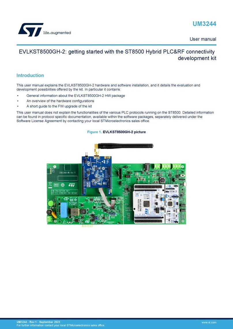
ST AEK-COM-ISOSPI1 User manual

introduction
One of the most commonly used communication protocols for device control is the SPI one. In the traditional vehicle
architecture, the SPI control is used to connect the device with the local microcontroller. With trends moving toward domain /
zone architectures, the local microcontroller is disappearing, therefore the protocol has to evolve to cover longer distances to
connect the device to the domain / zone controller. In addition, with electrification progressing inside the new vehicles, another
desirable feature for such a protocol is the electrical isolation. Based on these requirements, the isolated SPI (ISOSPI) protocol
has been defined.
The AEK-COM-ISOSPI1 board allows converting SPI signals into ISOSPI signals, reducing the number of necessary wires from
4 to 2, and ensuring an isolated differential communication highly immune to noise.
An ISOSPI signal can travel for several meters, maintaining a high ratio between signal and noise.
Figure 1. SPI to ISOSPI conversion block diagram
The ISOSPI protocol features differential communication to ensure higher noise immunity and robustness for long distance
communication. As the ISOSPI signals can travel for several meters, this protocol is particularly suitable for automotive high
voltage applications where electrical isolation is required by the safety standards and the cable length can affect the
communication among devices located in distant parts of the vehicle.
The AEK-COM-ISOSPI1 board is based on the L9963T integrated circuit, a general-purpose SPI to isolated SPI bi-directional
transceiver, which can transfer communication data incoming from a classical 4-wire based SPI interface to a 2-wire isolated
interface (and vice versa).
The L9963T hosted on the AEK-COM-ISOSPI1 can be configured either as a slave or as a master of the SPI bus and supports
any protocol of 8-to-64-bit SPI frames. The SPI peripheral can work up to 10 MHz when configured as a slave. The SPI clock
frequency can be programmed (250 kHz, 1 MHz, 4 MHz, or 8 MHz) when the device is configured as a master.
Getting started with the AEK-COM-ISOSPI1, SPI to isolated SPI dongle based on
the L9963T transceiver
UM3187
User manual
UM3187 - Rev 1 - June 2023
For further information contact your local STMicroelectronics sales office. www.st.com

The transceiver is natively compatible with the L9963E IC isolated SPI port, allowing its usage in battery management system
(BMS) applications. The basic BMS analog front-end node board is the AEK-POW-BMS63EN. From the microcontroller side,
the AEK-COM-ISOSPI1 board can be connected via SPI with SPC5, Stellar and STM32 microcontroller families.
Figure 2. AEK-COM-ISOSPI1
UM3187
UM3187 - Rev 1 page 2/35

1 Hardware overview
Figure 3. Hardware overview
SPI
CN1 - SDO
CN1 - SCK
CN1 - SDI
CN1 - NCS
Test points
Fault LED
DIS LED
BNE/CPOL LED
TXEN/CPHA LED
NSLAVE LED
CN2 - Fault
CN2 - DIS
CN2 - ISOFreq
CN2 - BNE/CPOL
CN2 - TXEN/CPHA
CN2 - TxAmp
CN2 - NSLAVE
SPI test points
L9963T
Galvanic coupling
JP1 NSLAVE
JP2 Txamp
JP3 TXEN
JP4 ISOfreq
JP5 BNE
JP6 DIS
CN3 - GND
CN3 - VIO (5 V)
CN3 - VDD (5 V)
CN3 - GND
JP1 NSLAVE
USB - ISOSPI
The AEK-COM-ISOSPI1 can be programmed through a microcontroller or using jumpers.
It is necessary to configure two parameters:
• The signal frequency
• The signal amplitude
To send a signal over a long distance, it is necessary to lower the frequency. Tune the signal frequency and
amplitude according to the distance that you intend to reach.
To set these parameters, use the jumpers for TxAmp and IsoFreq. They can be arranged in two positions: closing
pin 2 and pin 3 or closing pin 1 and pin 2.
Figure 4. Jumper configuration
Amplitude and frequency can be set through the microcontroller GPIO on the AEK-COM-ISOSPI1 DIS pin.
You can enable or disable the AEK-COM-ISOSPI1 through jumpers on the DIS pin or through the microcontroller.
UM3187
Hardware overview
UM3187 - Rev 1 page 3/35

Figure 5. Jumpers on DIS pin
To enable this pin, use jumpers on TXEN or program the microcontroller to set the TXEN pin.
Figure 6. TXEN pin
NSLAVE can assume the value 0 (for the slave configuration) or 1 (for the master configuration).
1.1 L9963T
The L9963T is a general purpose SPI to isolated SPI transceiver IC, which acts as a bridge among devices
located in different voltage domains.
The L9963T can transfer communication data incoming from a classical four-wire based SPI interface to a two-
wire isolated interface (and vice versa).
The device can be configured either as slave or as master of the SPI bus and supports any protocol made of SPI
frames (8 to 64 bits).
L9963T integrates two communication interfaces:
• a SPI interface used for the local data exchange with a master MCU or with a generic slave IC
• an isolated SPI interface for global/local isolated communication with another L9963T or with an ISOLine
compatible device (such as L9963E).
The SPI peripheral can work up to 10 MHz when configured as a slave.
The SPI clock frequency can be programmed (250 kHz, 1 MHz, 4 MHz, or 8 MHz) when configured as a master.
The isolated SPI peripheral features two different operating modes: slow at 333 kbps and fast at 2.66 Mbps.
The L9963T is compatible with both 3.3 V and 5 V logic.
1.2 Pin description
1.2.1 SPI
SDO, SCK, SDI, NCS pins implement the SPI peripheral, whose configuration depends on the NSLAVE value
latched at the first power-up:
• SDI is always configured as a digital input. It is internally pulled down with RIN_PD to generate a 0x0 frame
in case of pin loss (leading to CRC violation in safety applications). Its buffer is enabled only in the Normal
state.
UM3187
L9963T
UM3187 - Rev 1 page 4/35

• SDO is always configured as a digital output. Its buffer is enabled only if NCS is asserted. An external pull
up/pull down resistor defines the inactive level of the line.
• SCK, NCS can be either configured as a digital input (NSLAVE = 0, SPI slave) or as a digital output
(NSLAVE = 1, SPI master).
The selective enable/disable of the buffers helps reducing the power consumption of the device when the SPI
works at high frequencies.
1.2.2 CPOL and CPHA
The following table shows CPOL and CPHA settings according to different SPI modes.
Table 1. SPI mode configuration
SPI mode CPOL CPHA Shift SCK-Edge Capture SCK-Edge
0 0 0 Falling Rising
1 0 1 Rising Falling
2 1 0 Rising Falling
3 1 1 Falling Rising
Clock polarity has no significant effect on the transfer format. The commutation of this bit causes the inversion of
the clock signal (active high becomes active low and idle low becomes idle high). Clock phase settings, however,
allow selecting one of two different transfer times. The master configures the clock polarity (CPOL) and the clock
phase (CPHA) to be aligned with the slave device requirements. These parameters determine when data need to
be changed according to the clock line and which is the clock level when the clock is not active.
CPOL assigns a clock level when the clock is not active. The clock signal (SCK) can be inverted (CPOL = 1) or
not activated (CPOL = 0). For the inverted clock signal, the first clock edge is falling. For the first not inverted
clock signal, the first clock edge is rising.
CPHA is used to move the capture phase. If CPHA = 0, data are sampled on the leading (first) clock edge.
There are four possible modes that can be used in a SPI protocol:
1. For CPOL = 0, the clock basic value is zero. For CPHA = 0, data are sampled on the clock rising edge and
are shifted on the clock falling edge.
Figure 7. TXEN pin
UM3187
Pin description
UM3187 - Rev 1 page 5/35

2. For CPOL = 0, the clock basic value is zero. For CPHA = 1, data are sampled on the clock falling edge and
are shifted on the clock rising edge.
Figure 8. SPI protocol mode 1
3. For CPOL = 1, the clock basic value is 1. For CPHA = 0, data are sampled on the clock rising edge and are
shifted on the clock falling edge.
Figure 9. SPI protocol mode 2
UM3187
Pin description
UM3187 - Rev 1 page 6/35

4. For CPOL = 1, the clock basic value is 1. For CPHA = 1, data are sampled on the clock falling edge and
shifted on the clock rising edge.
Figure 10. SPI mode 3
1.2.3 NSLAVE
The NSLAVE pin is latched by the standby logic in the Trimming & Config Latch state. It must be either shorted to
VDD or to GND. The internal pull-down is enabled only while in Trimming & Config Latch state. This allows
reducing power consumption. Once Trimming & Config Latch state is left, the NSLAVE input buffer is permanently
disabled, since it is no longer needed.
NSLAVE selects the SPI master (NSLAVE = 1) or slave (NSLAVE = 0) operation and determines the digital I/Os
configuration.
To increase immunity to BCI and guarantee a correct latch of the NSLAVE pin during each power-up, the input is
filtered with an integrated RC filter.
1.2.4 DIS
DIS is a digital input-output pin that features an internal pull-up resistor towards V3V3_STBY. Its purpose is to be
driven by open-drain outputs. Its functionality is summarized as follows:
• Input: is an active high disabling input driven by the MCU:
– When DIS is released by the MCU longer than TRC_DELAY+TDIS_DEGLITCH, the device starts the
Go To Sleep sequence that brings the L9963T to the Stand-by state.
– When DIS is pulled down by the MCU longer than TRC_DELAY + (1/fSTBY_OSC), the device moves
from the Stand-by state to the Regulators enabling state and then to the Normal state.
• Output: when L9963T is in the Stand-by state, and a wake-up event by isolated SPI occurs, it moves to the
Regulators enabling state and then to the Normal state. Once the latter is reached, DIS is internally pulled
down by logic for TDIS_PULLDOWN to trigger an interrupt in the MCU or a wake-up event. After
TDIS_PULLDOWN expires, DIS is released and, if not kept low by an external source, the L9963T moves
back to the Stand-by state. To protect DIS internal open drain driver in case of external short to VDD, a
current limitation circuitry limits the current to IDIS_LIM.
1.2.5 BNE/CPOL
BNE/CPOL is a digital input/output pin whose configuration depends on the value of NSLAVE latched during
Trimming & Config Latch:
• When NSLAVE = 0 (slave configuration), this pin acts as BNE (buffer not empty) digital output. Its purpose
is to implement interrupt-based communication with the MCU. When asserted high, the RX queue stores at
least one frame.
UM3187
Pin description
UM3187 - Rev 1 page 7/35

• When NSLAVE = 1 (master configuration), this pin acts as a digital input for the selection of CPOL (clock
polarity):
– CPOL = 0 (shorted to GND) implies that the clock inactive level (when NCS is high) is low.
– CPOL = 1 (shorted to VDD) implies that the clock inactive level is high. The internal pull-down is
always enabled during Trimming & Config Latch and in Normal state. The BNE output buffer is
disabled if NSLAVE = 1 has been latched during Trimming & Config Latch. The CPOL input buffer is
permanently enabled.
In case NSLAVE = 0 has been latched during Trimming & Config Latch, BNE output buffer is kept enabled while in
the Normal state. A short to GND/VDD detection is implemented to protect the BNE output buffer. If the value
forced on the BNE output buffer differs from the one sampled by the CPOL input buffer for more than
TBNE_SHORT_DET, the BNE output buffer is put into HiZ. Automatic re-engagement of the BNE output buffer
occurs upon the next wakeup sequence (MCU needs to toggle DIS pin).
1.2.6 TXEN/CPHA
TXEN_CPHA is a digital input pin whose configuration depends on the value of NSLAVE latched during Trimming
& Config Latch:
• When NSLAVE = 0 (slave configuration) the pin works as a transmitter enabling TXEN:
– The MCU should release TXEN (or pull it up actively) prior to NCS assertion to enable the
transmission of the data from SDI input buffer to the TX queue (and then to the isolated SPI
interface).
– If the communication protocol does not feature any burst read capability, each command sent by the
master unit generates a single answer from the addressed slave unit. Hence, the TXEN pin can be
connected to VDD to keep the transmitter permanently enabled.
– In case of burst read operations, where the user software has to empty the RX queue without
transmitting any frame on the isolated SPI, the TXEN input must be pulled down before beginning the
burst read.
– Even if data on the SDI line is discarded while TXEN = 0, it is highly recommended that the MCU
sends dummy frames (or intentionally corrupted frames) on the SDI line during the burst read.
In the event of TXEN stuck high, such frames generate errors according to the implemented
communication protocol.
To avoid chopping frames currently being transmitted, the TXEN pin is latched upon NCS assertion.
Therefore, it must be stable at least TTXEN_DEGLITCH + TTXEN_SETUP before NCS assertion.
Moreover, TXEN must be kept stable TTXEN_HOLD after NCS assertion to fulfil hold time
constraints.
• When NSLAVE = 1 (master configuration), this pin acts as a digital input for the selection of CPHA (clock
phase). It is latched during Trimming & Config Latch and should be therefore either shorted to GND or to
VDD:
– CPHA = 0 (shorted to GND) implies that the SDI signal is sampled upon the first SCK edge after NCS
assertion.
– CPHA = 1 (shorted to VDD) implies that the SDI signal is sampled upon the second SCK edge after
NCS assertion.
The internal pull-up is enabled when L9963T is in Trimming & Config Latch and is kept enabled in the Normal
state to allow a correct driving of the pin by the open-drain output of the MCU. Moreover, in case of pin loss, the
pull-up guarantees a limp home operation where the transmitter is always enabled. To guarantee stand-by
consumption requirements, the pull-up is disabled while in the Stand-by state.
1.2.7 TXAMP
TXAMP pin can be used to switch between the two possible ISOline TX amplitude configurations:
• TXAMP = 0 selects low TX amplitude (RDIFF_ISO_OUTL)
• TXAMP = 1 selects high TX amplitude (RDIFF_ISO_OUTH)
TXAMP sampling depends on the device state and configuration.
UM3187
Pin description
UM3187 - Rev 1 page 8/35

Table 2. TXAMP sampling strategy
L9963T
state
L9963T
configuration TXAMP sampling Note
Normal
state
Slave (NSLAVE =
0)
The TXAMP pin is latched upon NCS assertion. Therefore, it
must be stable at least TTXAMP_DEGLITCH +
TTXAMP_SETUP before NCS assertion. Moreover, TXAMP
must be kept stable TTXAMP_HOLD after NCS assertion in
order to fulfil hold time constraints.
In case several SPI frames
are being pushed into the
TX queue, the setting
applied depends on the last
one latched (no pipelining
supported).
The new amplitude setting is applied to the TX interface after
the SPI frame has been completely transmitted over the
isolated SPI interface. This allows Managing ISOFREQ And
TXAMP Pins For Communicating With L9963.
Normal
state
Master (NSLAVE =
1)
The TXAMP setting is simply resynchronized
(TTXAMP_SETUP and TTXAMP_HOLD requirements still
apply) and deglitched (TTXAMP_DEGLITCH filter still present),
but it is not latched upon NCS assertion. The new amplitude
setting is applied to the TX interface as soon as the
transmission of the SPI frame over the isolated SPI interface
begins.
In case several SPI frames
are being pushed into the
TX queue, the setting
applied depends on the last
one latched (no pipelining
supported).
Stand-by
state
Slave/Master
(NSLAVE = X)
The new TXAMP setting is latched during the wakeup
sequence. Hence, the TXAMP pin shall be stable
TTXAMP_SETUP before the DIS high → low transition is
applied and shall not change during TWAKEUP.
-
Reset
state
Slave/Master
(NSLAVE = X)
The initial TXAMP setting is latched during the first power up
sequence. Hence, the TXAMP pin shall be stable before VDD
is applied and shall not change during TFIRST_POWERUP.
-
It is recommended to apply the same TXAMP settings to all the devices communicating on the bus, to keep a
constant SNR in every communication phase.
To meet stand-by consumption requirements, MCU must release the open drain output connected to TXAMP
while L9963T is in the Stand-by state.
1.2.8 SPICLKFREQ
SPICLKFREQ pin is an analog input, compared to four thresholds by a set of analog comparators.
An external resistor RCLKPD must be connected between SPICLKFREQ and GND, in order to generate a
voltage VSPICLKFREQ = RCLKPD * ISPICLKFREQPU.
The code obtained from these 4 comparator outputs is latched in the Trimming & Config Latch to determine the
SPI clock frequency when L9963T works in master mode (NSLAVE = 1).
In the AEK-COM-ISOSPI1 the SPICLKFREQ is fixed at 250 kHz.
1.2.9 ISOP and ISOM
The isolated SPI interface allows units with different ground levels and/or on different boards to communicate with
each other. Physically, the interface is based on twisted-pair wire.
Table 3. Pins used as isolated SPI
L9963T Pin SPI function Configuration
ISOP positive differential input/output Analog Input/Output
ISOM negative differential input/output Analog Input/Output
Table 4. Isolated SPI quick look
Parameter Description
Protocol Half-Duplex / Out of frame
Max. Bit-rate 2.66 Mbps (high speed configuration, ISOFREQ = 1)
UM3187
Pin description
UM3187 - Rev 1 page 9/35

Parameter Description
333 kbps (low speed configuration, ISOFREQ = 0, default if pin is left
floating)
The transmission line on the isolated SPI exploits a single twisted pair. Communication data is transmitted/
received over a pulse-shaped signal, in a half-duplex protocol.
Line bit rate can be selected by programming the ISOFREQ device pin.
A single bit is made of a pulse time (TPULSE) followed by two pauses (2TPULSE):
• TPULSE = 2TBIT_HIGH_LOW_FAST for the high speed configuration (ISOFREQ = 1)
• TPULSE = 2TBIT_HIGH_LOW_SLOW for the low speed configuration (ISOFREQ = 0)
An isolated receiver and transmitter are connected to the couple of pins and ISOP/M. Depending on the
communication phase, they can be enabled or disabled.
The receiver can convert a differential input signal into a single ended signal that is provided to the logic:
• While in Normal state, to guarantee correct communication, the input common mode must stand within
VCM_ISO_IN limits.
• When in Stand-by state, the ISOP and ISOM pins are not biased with a common mode. If the device
receives a series of differential pulses longer than NMIN_ISO_WAKEUP_EDGES, a wakeup condition is
triggered. Pulse amplitude must be higher than Wakeup_thr to be counted.
1.2.10 ISOFREQ
ISOFREQ pin is a digital input used to switch ISOline bit rate:
• ISOFREQ = 1 selects fast operation: bit time is TBIT_LENGTH_FAST
• ISOFREQ = 0 selects slow operation: bit time is TBIT_LENGTH_SLOW
ISOFREQ sampling depends on device state and configuration.
Table 5. ISOFREQ sampling strategy
L9963T
state
L9963T
configuration ISOFREQ sampling Note
Normal
state
Slave (NSLAVE =
0)
The ISOFREQ pin is latched upon NCS assertion. Therefore,
it must be stable at least TISOFREQ_DEGLITCH +
TISOFREQ_SETUP before NCS assertion. Moreover,
ISOFREQ must be kept stable TISOFREQ_HOLD after NCS
assertion in order to fulfil hold time constraints. In case several SPI frames
are being pushed into the TX
queue, the setting applied
once the TX interface is in idle
depends on the last one
latched (no pipelining
supported).
The new bit rate setting is immediately applied to the RX
interface, while it is applied to the TX interface after the SPI
frame has been completely transmitted over the isolated SPI
interface. This allows Managing ISOFREQ And TXAMP Pins
For Communicating With L9963
Master (NSLAVE =
1)
The ISOFREQ setting is simply resynchronized
(TISOFREQ_SETUP and TISOFREQ_HOLD requirements
still apply) and deglitched (TISOFREQ_DEGLITCH filter still
present), but it is not latched upon NCS assertion.
Stand-by
state
Slave/Master
(NSLAVE = X)
The new ISOFREQ setting is latched during the wake up
sequence. Hence, the ISOFREQ pin shall be stable
TISOFREQ_SETUP before the DIS high → low transition is
applied and shall not change during TWAKEUP.
-
Reset
state
Slave/Master
(NSLAVE = X)
The initial ISOFREQ setting is latched during the first power
up sequence. Hence, the ISOFREQ pin shall be stable
before VDD is applied and shall not change
duringTFIRST_POWERUP.
-
UM3187
Pin description
UM3187 - Rev 1 page 10/35

2 Power supply
The figure below lists the product power supply ranges.
Figure 11. Power supply ranges
• Within the range of functionality, the part operates as specified and without parameter deviations. All the
functionalities and the electrical parameters are guaranteed.
• If either the upper or the lower limited operating range is reached, the device may not operate properly.
Only a limited set of functionalities and electrical parameters are guaranteed. However, neither damage nor
parameter deviation occurs, and the device operates properly once returned to the range of functionality.
• If the absolute maximum rating (AMR) is violated, permanent damage or parametric deviation may occur.
Note: All voltages are related to the potential at substrate ground GND.
UM3187
Power supply
UM3187 - Rev 1 page 11/35

3 Finite state machine
Figure 12. Finite state machine
configuration latch
Trimming and
When DIS pin is released for
Device is powered up by VDD
Power on reset negative released
POR_MAIN asserted
Normal
Stand-by
Reset
Regulators
enabling
Regulators
at least Trc_delay + Tdis_deglitch
disabling
Wakeup event (DIS pin pulled down or
ISOline activity) or FirstPowerupDone = 0
FirstPowerupDone = 0
POR_MAIN released
FirstPowerupDone = 1
POR_MAIN released
Different state transition sequences occur according to the following different scenarios:
• First power-up: Reset state → Stand-by state → Regulators enabling state → Trimming & Config Latch →
Normal state. The first power-up sequence lasts TFIRST_POWERUP.
• Wake up: Stand-by state → Regulators enabling state → Normal state. In case of wakeup triggered by DIS
release, the state transition is the same. The wakeup sequence lasts TWAKEUP.
• Go To Sleep: Normal state → Regulators disabling state → Stand-by state. The go to sleep sequence lasts
TGO2SLP.
3.1 Reset state
When VDD is below the value triggering the power-up, the device is not functional. No operation is possible while
under reset.
3.2 Stand-by state
This state is entered either from the Reset state or from the Regulators disabling state:
• Transition from the Regulators disabling state only occurs upon DIS low → high transition while L9963T is
in the Normal state. DIS input signal is filtered in both analog (TRC_DELAY) and digital (TDIS_DEGLITCH)
domains.
• Transition from Reset state only occurs upon first power-up, after POR_STBY release.
While in standby, the logic checks the FirstPowerupDone latch, whose reset value is ‘0’ upon the first power-up:
• In case FirstPowerupDone = 0, the first power-up has never been accomplished. Hence, the device moves
to the Regulators enabling state, regardless of any wakeup source state.
• In case FirstPowerupDone = 1, the first power-up has already been accomplished. Hence, the device is
kept in the Stand-by state and eventual transitions are determined by the wakeup sources.
When a wakeup source is asserted, it triggers the wakeup sequence that moves the L9963T to the Regulators
enabling state. The possible wakeup sources are:
• The de-assertion of DIS pin, pulled down by an external open drain source (TRC_DELAY + (1/
fSTBY_OSC) filter applies).
• The detection of at least NMIN_ISO_WUP_EDGES pulses within TWAKEUP_TIMEOUT_ISO on the
ISOline.
3.3 Regulators enabling state
This is a transitional state reached from the Stand-by state.
While L9963T is in this state, it enables the V3V3 regulator and the OSCI_MAIN.
During this process lasting TWAKEUP, the device must not be sensitive to DIS pin, SPI interface, and ISOline
sources. Once a wakeup sequence starts, it cannot be interrupted.
UM3187
Finite state machine
UM3187 - Rev 1 page 12/35

The Regulators enabling state is left upon Fs_MAIN release. The next state depends on the FirstPowerupDone
latch:
• In case FirstPowerupDone = 0, the first power-up has never been accomplished. Hence, the device moves
to the Trimming & Config Latch.
• In case FirstPowerupDone = 1, the first power-up has already been accomplished. Hence, the device
moves to the Normal state.
3.4 Trimming and configuration latch state
This state is entered from the Regulators enabling state the first time the device is powered up
(FirstPowerupDone = 0).
While in this state, the device must:
• Download the OTP data.
• Latch the configuration inputs (NSLAVE, CPHA, CPOL, SPICLKFREQ), storing them into the STBY logic
registers.
SPICLKFREQ comes from a set of comparators that must be checked by an internal BIST before latching the
comparator output. In case the BIST fails, a default 0 value (corresponding to the slowest SPI configuration) must
be stored into the related stand-by internal register.
Stand-by registers hold their value as long as the POR_STBY stays de-asserted.
While in this state, L9963T is not sensitive to SPI/VIF activity and wakeup conditions (DIS/VIF).
This phase must safely go to an end and may last a maximum time interval of TSETUP_LATCH.
After this phase finishes, the FirstPowerupDone latch is set to "1" in the standby logic and the device moves to
the Normal state.
3.5 Normal state
While in this state, all references and main logic are powered. Both communication interfaces are ready for data
TX/RX activity.
This state is reached either from Trimming & Config Latch (first power up) or from Regulators enabling state
(following a normal wakeup sequence):
• When woken up by an activity on the ISOline, once the Normal state is reached, the device must neglect
the DIS pin value (even if it is high) and, on the contrary, it must drive the DIS pin low for
TDIS_PULLDOWN (DIS is an input/output pin). Such a strategy allows generating an interrupt into the
MCU, or triggering a wakeup. Once TDIS_PULLDOWN expires, L9963T releases the DIS pull down and
unmasks the DIS deglitched input. If the MCU has been correctly woken up, it pulls down the DIS pin
externally, so that L9963T is kept in the Normal state.
Otherwise, DIS is found asserted (high) and the IC moves back to the Regulators disabling state.
• When woken up by the DIS pin itself, the device must start listening to the deglitched DIS pin as soon as it
enters the Normal state.
To detect a "Go to Sleep" condition, the DIS pin status must be constantly monitored through a synchronous
deglitch filter (TDIS_DEGLITCH, implemented in the main logic through the main oscillator).
Its effect is cascaded to the passive RC filter placed on the input comparator (TRC_DELAY).
When DIS is sensed "high", the main logic raises a signal that triggers the “Go To Sleep” sequence in the IC FSM.
L9963T moves to the Regulators disabling state and finally to the Stand-by state.
3.6 Regulators disabling state
This is a transitional state reached from the Normal state during a "Go To Sleep" sequence.
While in this state, the V3V3_MAIN regulator and main oscillator enable signals are de-asserted, leading to
POR_MAIN assertion and reset of the main logic.
POR_MAIN assertion marks the transition to the Stand-by state.
Even if the main logic is still alive while the device is in the Regulators disabling state, it must not be sensitive to
external pins (wakeup sources, COM interfaces, etc.). Once started, a "Go To Sleep" sequence cannot be
interrupted.
UM3187
Trimming and configuration latch state
UM3187 - Rev 1 page 13/35

4 AutoDevKit ecosystem
The application development employing the AEK-COM-ISOSPI1 board takes full advantage of the AutoDevKit
ecosystem, whose basic components are:
• AutoDevKit Studio IDE (STSW-AUTODEVKIT)
•PLS UDE and OpenOCD programmers and debuggers
4.1 Component folder structure
Figure 13. AEK-COM-ISOSPI1 component folder structure
The cfg folder contains all the configuration files.
The doc folder contains the doxygen documentation.
The lib folder contains the component header and source files.
4.2 Software component architecture (AEK-COM-ISOSP1 Component RLA)
The following image shows the architecture of the software components that we created for the AEK-COM-
ISOSPI1 evaluation board, which consists of the following layer:
• AEK-COM-ISOSPI1_lld
Figure 14. Software architecture
The AEK-COM-ISOSP1_lld contains all the APIs:
• To configure L9963T transceiver as a master or a slave SPI.
• To configure amplitude and frequency of the ISOSP1 signal.
• To enable/disable the L9963T transceiver.
• To enable/disable ISOSPI communication.
UM3187
AutoDevKit ecosystem
UM3187 - Rev 1 page 14/35

5 Available APIs
The APIs listed in the following tables are declared in the “AEK_COM_ISOSPI1_lld.h” file.
Table 6. APIs for the AEK-COM-ISOSPI1
API name Description
l9963t_PALWritePad (ISOSPI_Driver_t l9963t, ISOSPI_pal_ch_t
l9963t_pal_ch, uint8_t value) Sets the logical state of a pad of the AEK-COM-ISOSPI1.
l9963t_PALReadPad (ISOSPI_Driver_t l9963t, ISOSPI_pal_ch_t
l9963t_pal_ch) Reads the logical state of a pad of the AEK-COM-ISOSPI1.
AEK_COM_ISOSPI_SetAsSlave (ISOSPI_DEVICE dev) Sets the AEK-COM-ISOSPI1 as a slave.
AEK_COM_ISOSPI_EnableTransceiverComm (ISOSPI_DEVICE
dev) Enables the transceiver communication.
AEK_COM_ISOSPI_DisableTransceiverComm (ISOSPI_DEVICE
dev) Disables the transceiver communication.
AEK_COM_ISOSPI_SetAsMaster (ISOSPI_DEVICE dev) Sets the AEK-COM-ISOSPI1 as a master.
AEK_COM_ISOSPI_SampleSPI_firstclk (ISOSPI_DEVICE dev) Samples the SPI first clock.
AEK_COM_ISOSPI_SampleSPI_secondclk (ISOSPI_DEVICE dev) Samples the SPI second clock.
AEK_COM_ISOSPI_CPOL_low (ISOSPI_DEVICE dev) Sets CPOL low (this function can be used only if NSLAVE = 1).
AEK_COM_ISOSPI_CPOL_high (ISOSPI_DEVICE dev) Sets CPOL high (this function can be used only if NSLAVE = 1).
AEK_COM_ISOSPI_EnableTransceiver (ISOSPI_DEVICE dev) Enables the transceiver.
AEK_COM_ISOSPI_DisableTransceiver (ISOSPI_DEVICE dev) Disables the transceiver.
AEK_COM_ISOSPI_SetISOCommSlow (ISOSPI_DEVICE dev) Sets the ISOFREQ to low (this establishes a slow communication equal
to 333 kHz).
AEK_COM_ISOSPI_SetISOCommFast (ISOSPI_DEVICE dev) Sets the ISOFREQ to high (this establishes a fast communication equal
to 2.66 MHz).
AEK_COM_ISOSPI_ISOTX_Attenuate (ISOSPI_DEVICE dev) Sets TXAMP to low (SPI signal not amplified).
AEK_COM_ISOSPI_ISOTX_Amplify (ISOSPI_DEVICE dev) Sets TXAMP to high (SPI signal amplified).
AEK_COM_ISOSPI_GetFault (ISOSPI_DEVICE dev) Reads the value of the FAULT pin and updates a fault flag, which is
included in the driver data structure (ISOSPI_Driver_t).
AEK_COM_ISOSPI_ConfigMode (ISOSPI_DEVICE dev,
ISOSPI_mode_t l9963t_mode) Configures the NSLAVE according to the user interface configuration.
AEK_COM_ISOSPI_ConfigISOFreq (ISOSPI_DEVICE dev,
ISOSPI_iso_freq_t l9963t_iso_freq) Configures the ISOFREQ according to the user interface configuration.
AEK_COM_ISOSPI_ConfigISOAmp (ISOSPI_DEVICE dev,
ISOSPI_tx_amp_t l9963t_tx_amp) Configures the TXAMP according to the user interface configuration.
AEK_COM_ISOSPI_ConfigCPOL (ISOSPI_DEVICE dev,
ISOSPI_master_cpol_t l9963t_cpol) Configures the CPOL according to the user interface configuration.
AEK_COM_ISOSPI_ConfigCPHA (ISOSPI_DEVICE dev,
ISOSPI_master_cpha_t l9963t_cpha) Configures the CPHA according to the user interface configuration.
config_Transceiver (ISOSPI_Driver_t driver) Comprehensive API, invoking ConfigMode, ConfigISOFreq,
ConfigISOAmp, ConfigCPOL, ConfigCPHA functions.
slave_example_config (ISOSPI_DEVICE dev) Slave configuration function example, which drives every configuration
pin of the transceiver setting it as a slave.
master_example_config (ISOSPI_DEVICE dev) Master configuration function example, which drives every configuration
pin of the transceiver setting it as a master.
UM3187
Available APIs
UM3187 - Rev 1 page 15/35

6 Using AEK-COM-ISOSP1 within AutoDevKit
In this example, we created an application for the AEK-COM-ISOSP1 configured as a slave transceiver. We used
the AEK-MCU-C4MLIT1 as the microcontroller board.
To recreate this scenario, follow the procedure below.
Step 1. Create a new SPC5-STUDIO application for the SPC58EC series microcontroller and add the following
components:
– SPC58ECxx Init Package Component RLA
– SPC58ECxx Low Level Drivers Component RLA
– AutoDevKit Init Package Component
These components must be added immediately, or the other components will not be visible.
Figure 15. Adding components
Step 2. Add the following additional components
– AEK-COM-ISOSPI1 Component RLA
Figure 16. Adding components
UM3187
Using AEK-COM-ISOSP1 within AutoDevKit
UM3187 - Rev 1 page 16/35

Step 3. Select [AEK-COM-ISOSPI1 Component RLA] to open the [Application Configuration] window.
Figure 17. Adding components
Step 4. Click on [+] to add a new element to the board list.
Figure 18. Adding components
UM3187
Using AEK-COM-ISOSP1 within AutoDevKit
UM3187 - Rev 1 page 17/35

Step 5. Double-click on the newly added element to configure the board.
Figure 19. AEK-COM-ISOPI1 configuration
UM3187
Using AEK-COM-ISOSP1 within AutoDevKit
UM3187 - Rev 1 page 18/35

Step 6.
– Select scenario “two”
– Select DSPI and CS
– Select the “cfg” configuration as “micro”
– Select TxAmp as “not amplified”
– Select ISOFreq as “333 KHz”
– Select Master Clock Frequency as “5 MHz”
– Select CPOL and CPHA as “low”
Figure 20. Available scenarios
UM3187
Using AEK-COM-ISOSP1 within AutoDevKit
UM3187 - Rev 1 page 19/35

Figure 21. AEK-COM-ISOPI1: scenario number two configuration
Step 7. Click on the “Allocation” button to allocate the AEK-POW-ISOSPI1 component.
Figure 22. Component allocation
Step 8. Click on “Board View” to see Hardware connection between the AEK-MCU-C4MLIT1 board and the
AEK-COM-ISOSP1 dongle.
Figure 23. Hardware connection through the Board View
UM3187
Using AEK-COM-ISOSP1 within AutoDevKit
UM3187 - Rev 1 page 20/35
Table of contents
Other ST Computer Hardware manuals

ST
ST B-WB1M-WPAN1 User manual

ST
ST UM2727 User manual

ST
ST X-NUCLEO-SNK1M1 User manual

ST
ST EVALSPEAr320HMI User manual

ST
ST STM32F10 Series Installation and operating instructions

ST
ST UM2960 User manual

ST
ST X-CUBE-CELLULAR User manual

ST
ST STSW-ST25DV002 User manual

ST
ST STM32F411 User manual

ST
ST X-NUCLEO-GFX01M1 User manual
Popular Computer Hardware manuals by other brands

hopf Elektronik GmbH
hopf Elektronik GmbH 8030NTS/NCD Technical manual

Seagate
Seagate ST3000VX005 product manual

Dolby Laboratories
Dolby Laboratories CP500 user manual

Acconeer
Acconeer XE132 Getting started guide

Espressif Systems
Espressif Systems ESP8684 Series Hardware Design Guidelines

Renesas
Renesas Single-Chip Microcomputer SH7203 Hardware manual