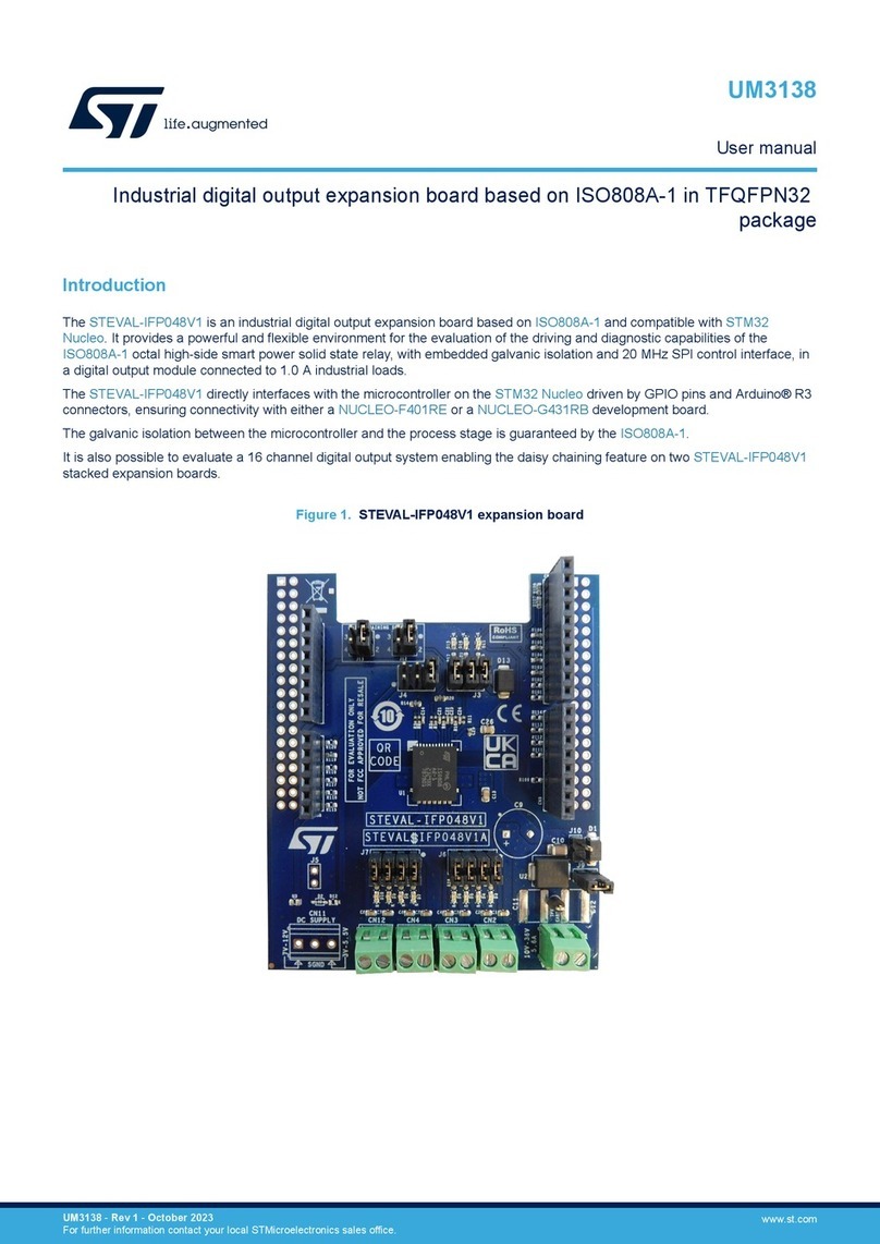
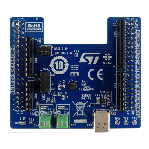
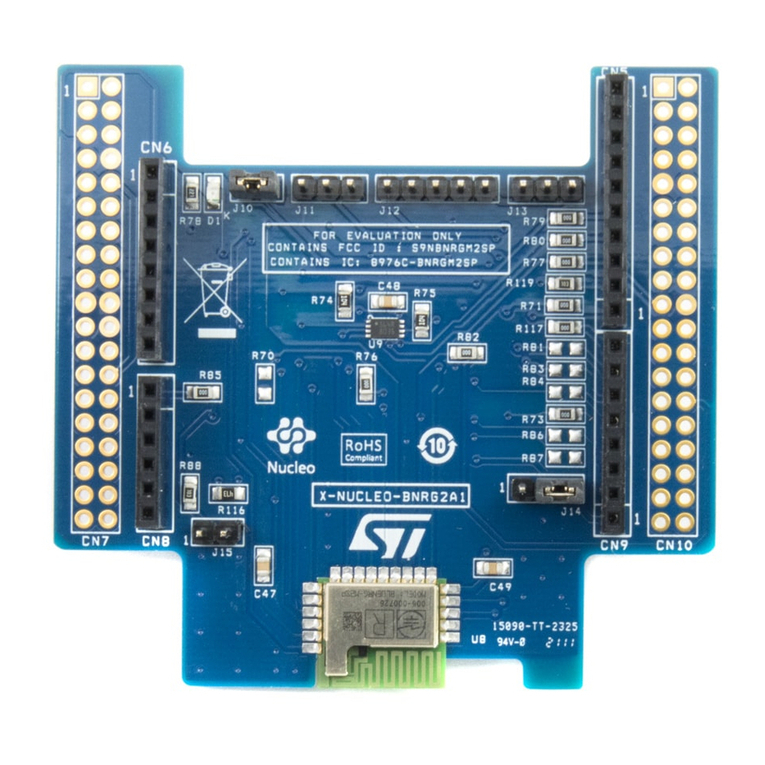
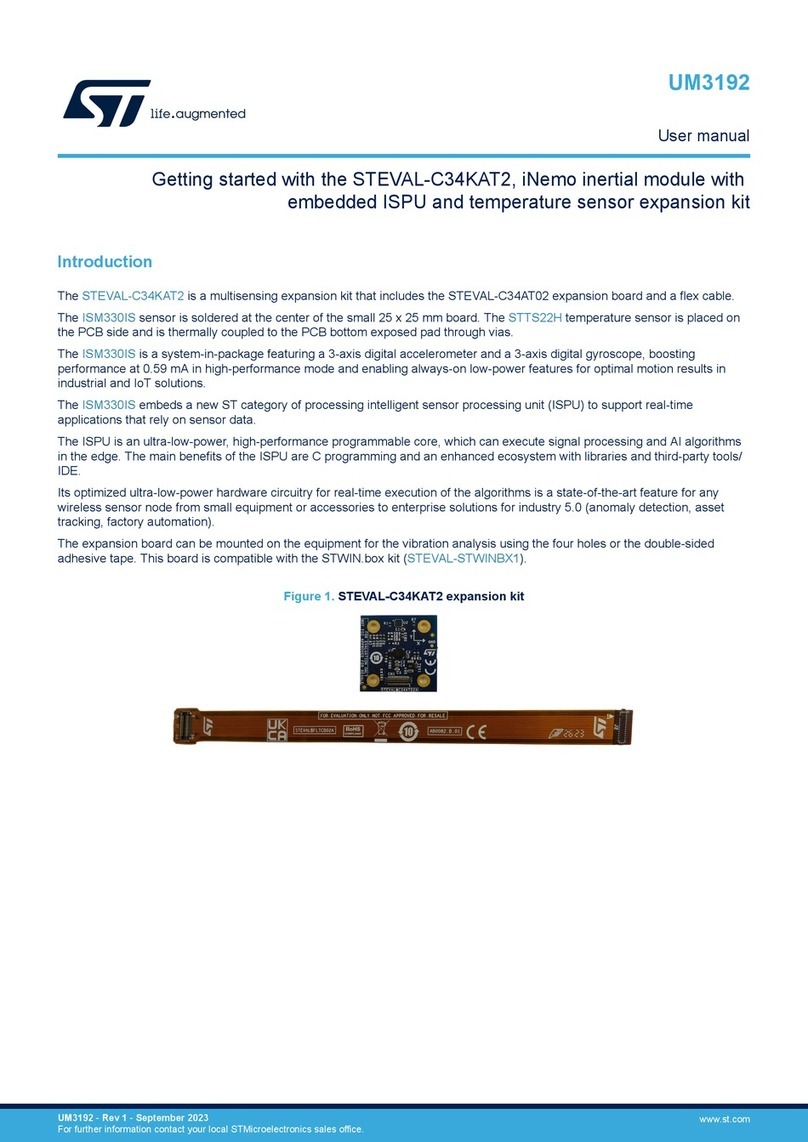
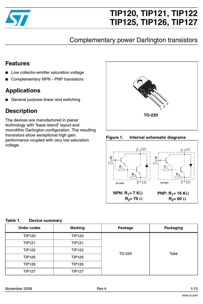
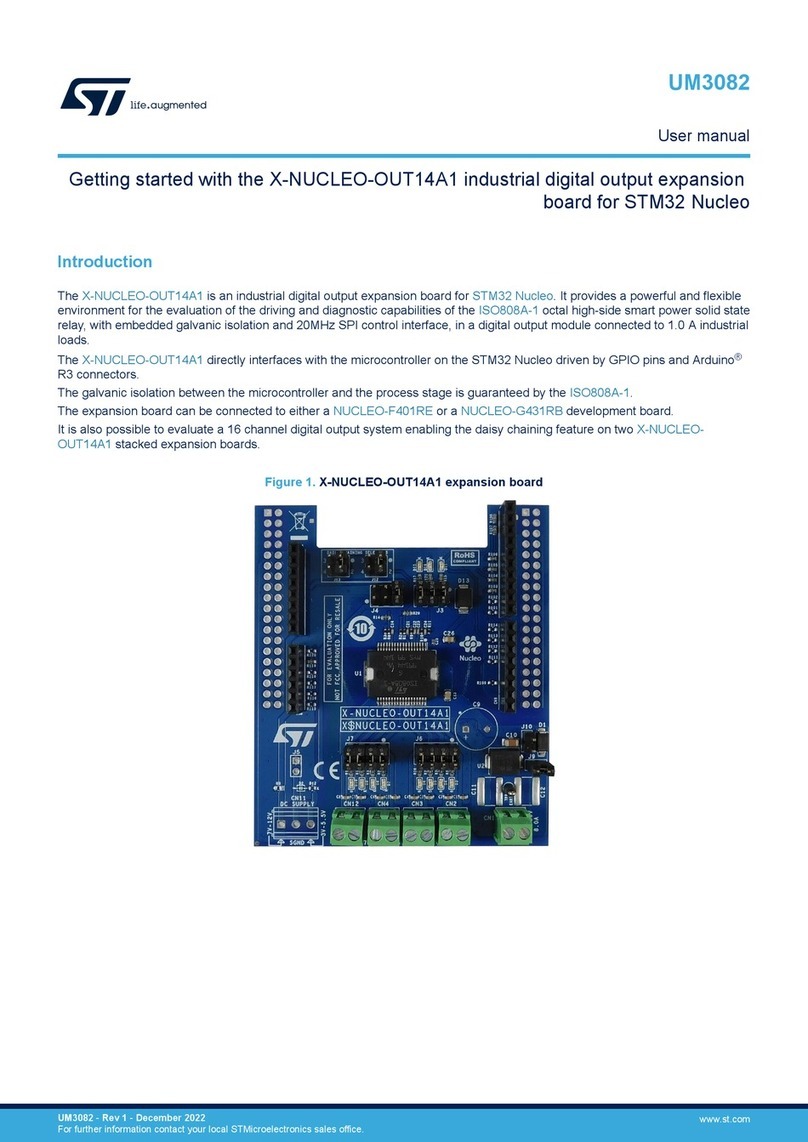
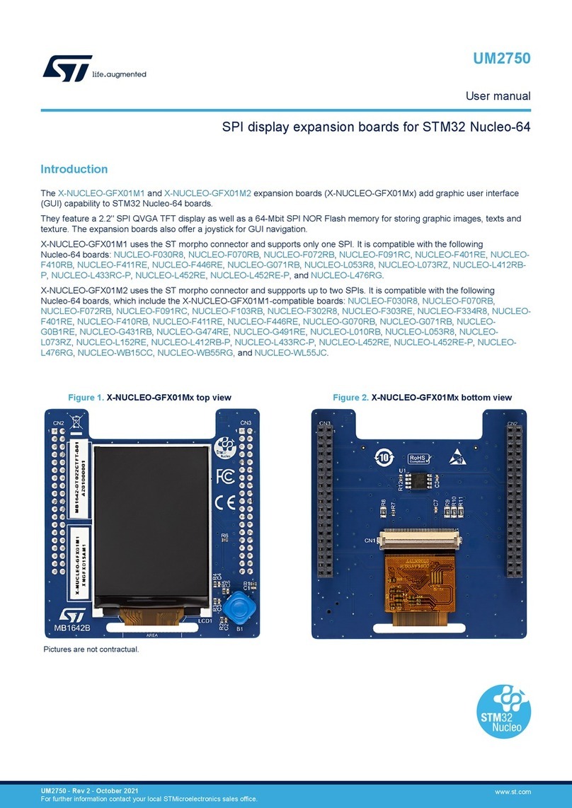
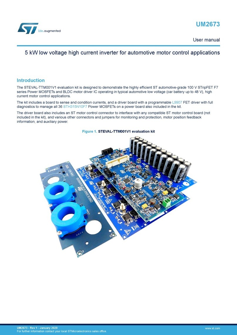
ST STM32U5G9J-DK2 User manual

Introduction
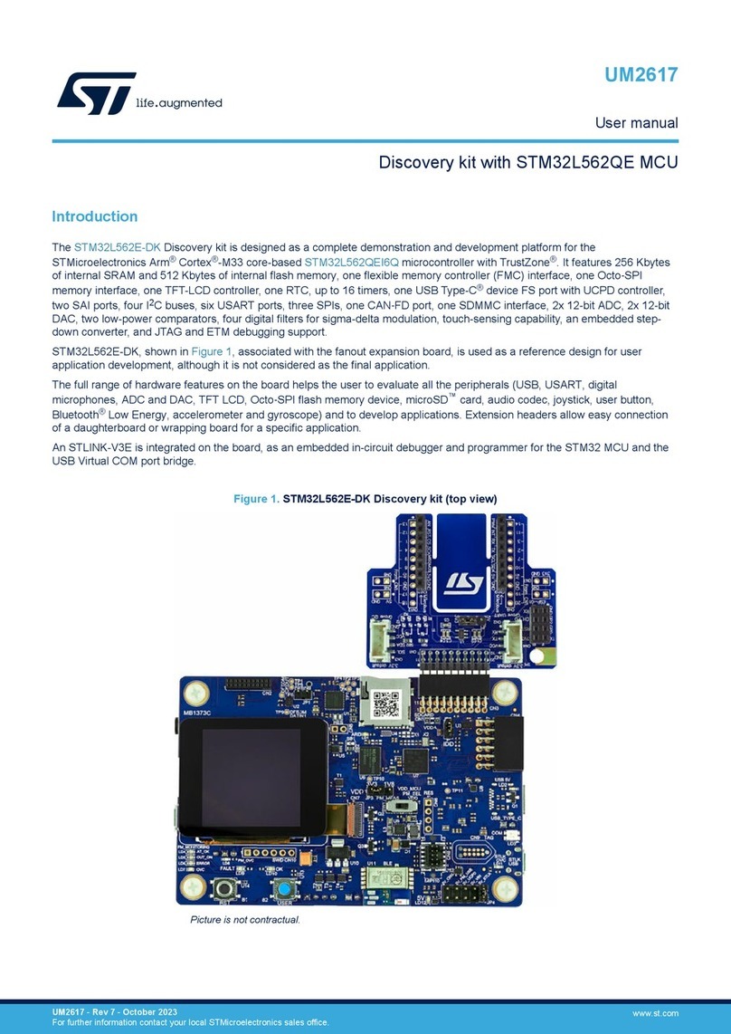
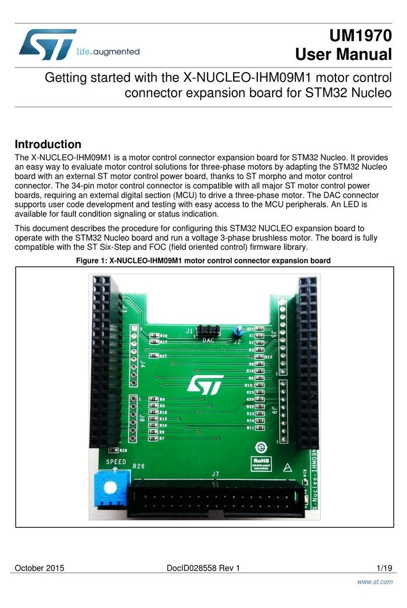
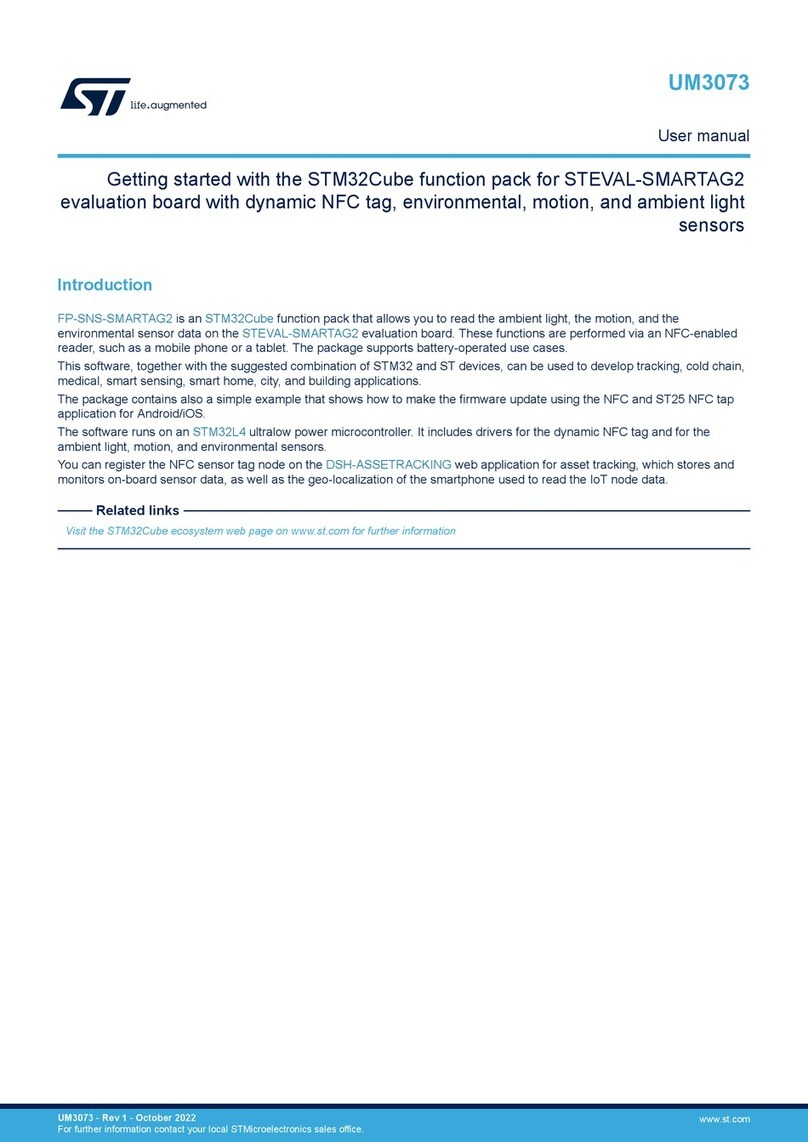
The STM32U5G9J-DK2 Discovery kit is a complete demonstration and development platform for the STM32U5G9ZJT6Q
microcontroller, featuring an Arm® Cortex®‑M33 core with Arm® TrustZone®.
Leveraging the innovative ultra-low power-oriented features, 3 Mbytes of embedded SRAM, 4 Mbytes of embedded flash
memory, and rich graphics features, the STM32U5G9J-DK2 Discovery kit enables users to prototype applications with
state‑of‑the‑art energy efficiency, as well as providing stunning and optimized graphics rendering with the support of a 2.5D
Neo-Chrom accelerator, Chrom-ART Accelerator, and Chrom-GRC™ MMU.
The STM32U5G9J-DK2 Discovery kit integrates a full range of hardware features that help the user evaluate all the peripherals,
such as a 5" RGB 800x480 pixels TFT colored LCD module with a 24‑bit RGB interface and capacitive touch panel, high-speed
USB Type-C®, Octo‑SPI flash memory device, ARDUINO®, and STLINK-V3EC (USART console).
The STM32U5G9J-DK2 Discovery kit integrates an STLINK-V3EC embedded in-circuit debugger and programmer for the
STM32 microcontroller with a USB Virtual COM port bridge and comes with the STM32CubeU5 MCU Package, which provides
an STM32 comprehensive software HAL library as well as various software examples.
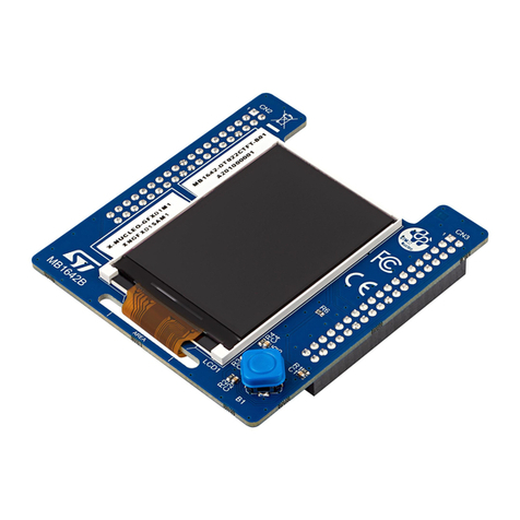
Figure 1. STM32U5G9J-DK2
with LCD (top view)
Figure 2. STM32U5G9J-DK2
without LCD (top view)
Figure 3. STM32U5G9J-DK2
(bottom view)
Pictures are not contractual.
Discovery kit with STM32U5G9ZJ MCU
UM3223
User manual
UM3223 - Rev 1 - January 2024
For further information contact your local STMicroelectronics sales office. www.st.com

1 Features
• Ultra-low-power STM32U5G9ZJT6Q microcontroller based on the Arm® Cortex®‑M33 core with Arm®
TrustZone®, featuring 4 Mbytes of flash memory, 3 Mbytes of SRAM, and SMPS, in an LQFP144 package
• 5" 800 × 480 pixels TFT LCD module with 16.7M color depth, parallel RGB interface, and capacitive touch
panel
• USB Type-C® with USB 2.0 high-speed interface, UCPD Sink only
• Low-power system designed for VDD at 3.3 V only
• 1-Gbit Octo‑SPI flash memory
• Two user LEDs
• User and reset push-buttons
• Board connectors:
–ST-LINK USB Type-C®
–User USB Type-C®
–Arm® Cortex® MIPI10 connector (SWD/JTAG/trace)
–Tag‑Connect™ 10-pin footprint
–ARDUINO® Uno V3 expansion
– Double-row 2.54 mm pitch expansion connector for additional peripherals prototyping
• On-board STLINK-V3EC debugger/programmer with USB re-enumeration capability: mass storage, Virtual
COM port, and debug port
• Comprehensive free software libraries and examples available with the STM32CubeU5 MCU Package
• Support of a wide choice of Integrated Development Environments (IDEs) including IAR Embedded
Workbench®, MDK-ARM, and STM32CubeIDE
Note: Arm and TrustZone are registered trademarks of Arm Limited (or its subsidiaries) in the US and/or elsewhere.
UM3223
Features
UM3223 - Rev 1 page 2/37

2 Ordering information
To order the STM32U5G9J-DK2 Discovery kit, refer to Table 1. Additional information is available from the
datasheet and reference manual of the target STM32.
Table 1. List of available products
Order code Board reference Target STM32
STM32U5G9J-DK2 • MB1918(1)
• MB1860(2) STM32U5G9ZJT6Q
1. Main board
2. LCD daughterboard
2.1 Codification
The meaning of the codification is explained in Table 2.
Table 2. Codification explanation
STM32XXYYZ-DKT Description Example: STM32U5G9J-DK2
XX MCU series in STM32 32-bit Arm Cortex MCUs STM32U5 series
YY MCU product line in the series STM32U5F9/5G9 product line
ZSTM32 flash memory size:
• J for 4 Mbytes 4 Mbytes
DK Discovery kit Discovery kit
T Sequential number Second Discovery kit version
UM3223
Ordering information
UM3223 - Rev 1 page 3/37

3 Development environment
3.1 System requirements
•Multi‑OS support: Windows® 10, Linux® 64-bit, or macOS®
• USB Type-A or USB Type-C® to USB Type-C® cable
Note: macOS® is a trademark of Apple Inc., registered in the U.S. and other countries and regions.
Linux® is a registered trademark of Linus Torvalds.
Windows is a trademark of the Microsoft group of companies.
3.2 Development toolchains
•IAR Systems® - IAR Embedded Workbench®(1)
•Keil® - MDK-ARM(1)
• STMicroelectronics - STM32CubeIDE
1. On Windows® only.
3.3 Demonstration software
The demonstration software, included in the STM32Cube MCU Package corresponding to the on-board
microcontroller, is preloaded in the STM32 flash memory for easy demonstration of the device peripherals in
standalone mode. The latest versions of the demonstration source code and associated documentation can be
downloaded from www.st.com.
UM3223
Development environment
UM3223 - Rev 1 page 4/37

4 Conventions
Table 3 provides the conventions used for the ON and OFF settings in the present document.
Table 3. ON/OFF convention
Convention Definition
Jumper JPx ON Jumper fitted
Jumper JPx OFF Jumper not fitted
Jumper JPx [1-2] Jumper fitted between Pin 1 and Pin 2
Solder bridge SBx ON SBx connections closed by 0 Ω resistor
Solder bridge SBx OFF SBx connections left open
Capacitor Cx ON Capacitor soldered
Capacitor Cx OFF Capacitor not soldered
UM3223
Conventions
UM3223 - Rev 1 page 5/37

5 Quick start
Before installing and using the product, accept the evaluation product license agreement from the www.st.com/
epla webpage.
Follow the sequence below to configure the STM32U5G9J-DK2 Discovery board and launch the demonstration
application (refer to Figure 5 for component location):
1. For the correct identification of all the device interfaces from the host PC and before connecting the board,
install the STLINK-V3EC USB driver available on the www.st.com website.
2. Check that the JP1 jumper (5V power source selection) is set on [1-2] selecting 5V from STLINK-V3EC
(STLK) and JP4 (VDD_MCU current measurement) is ON powering the microcontroller. Refer to Table 4.
3. Connect the STM32U5G9J-DK2 Discovery board to a PC with a USB cable (USB Type-A or USB Type-C® to
USB Type-C®) through the STLINK-V3EC USB connector (CN8) to power the board.
4. Then, the 5V_PWR green LED (LD1) lights up and the COM LED (LD7) blinks.
5. The LCD module displays a menu with icons, indicating the demonstration application software startup.
6. The demonstration application software and its user manual, as well as other software examples for exploring
STM32U5G9J-DK features are available on the STM32CubeU5 webpage.
7. Develop your application using the available examples.
Table 4. Default jumper setting
Jumper Function Setting(1) Comment
JP1 5 V power source selection [1-2] 5 V from STLINK-V3EC (STLK)
JP4 IDD measurement ON VDD_MCU current measurement
1. The default setting is in bold.
UM3223
Quick start
UM3223 - Rev 1 page 6/37

6 Hardware layout and configuration
6.1 Hardware block diagram
The STM32U5G9J-DK2 is designed around the STM32U5G9ZJT6Q microcontroller in an LQFP144 package. The
hardware block diagram in Figure 4 illustrates the connection between the STM32U5G9ZJT6Q microcontroller
and the peripherals. Figure 5 and Figure 6 show the locations of these features on the STM32U5G9J-DK2
Discovery board.
Figure 4. STM32U5G9J-DK2 hardware block diagram
DT59217V1
STLINK_V3EC
USB Type-C®
Octo-SPI
16MHz
crystal
32 KHz
crystal
ARDUINO® Uno
V3 connector
Boot switch
User button
Reset button
Red user LED
Green user LED
5" LCD
capacitive
touch panel
(MB1860 on
RGB connector)
USB Type-C®
connector
External debug
MIPI10 and
Tag-Connect™
SWD/JTAG
4
4
4
UART
22
Hexa-SPI
11
BOOT0
1
LCD
I2C 2
GPIO 1
RGB888 and ctrl
Touch panel
ON/OFF
Backlight
Touch-panel
interrupt
PWM
GPIO
GPIO 1
GPIO 1
GPIO 1
NRST
USB DP/DM USB DP/DM
OCTOSPI
Reset
Reset
Reset
SWD/
JTAG
UART
SWD/JTAG
Reset
ADCs
ADC/I2C
I2C
UART
ADCs
ADC/
I2C
2
4
I2C
2
PWM
UART
2
PWM
4
GPIOs GPIOs
4
PWM
SPI
PWM 1
SPI
OSC32K
2
OSC
2
Discrete
components
DC/DC 3V3 power supply
Extension connector
GPIOs 16
STM32U5G9ZJT6Q
1
1
2
3
28
1
UM3223
Hardware layout and configuration
UM3223 - Rev 1 page 7/37

6.2 Main board layout
Figure 5. Main board layout (top view)
DT59218V1
STLK_NRST
header (JP3)
STLINK_V3EC
(U13)
STLINK USB
(CN8)
Power source
header (JP1)
USB Type-C®
connector (CN2)
TCPP01-M12 USB
protection (U3)
Reset button
(B1)
MIPI10 connector
(CN11)
Octo-SPI flash memory
(U11)
BOOT0 switch
(SW1)
IDD MCU
(JP4)
STM32U5G9 MCU
(U2)
ARDUINO® connectors
(CN4, CN5, CN6, CN7)
Spare GPIO
connector (CN1)
Figure 6. Main board layout (bottom view)
DT59219V1
RGB LCD connector
(CN3)
Tag-Connect™
footprint (CN10)
ST-LINK COM LED (LD7)
5V power LED (LD1)
5V USB power (LD5)
User red LED (LD2)
User green LED (LD3)
User button (B2)
ST-LINK power LED (LD6)
UM3223
Hardware layout and configuration
UM3223 - Rev 1 page 8/37

6.3 Mechanical drawing
Figure 7. Main board mechanical drawing (in millimeters)
UM3223
Hardware layout and configuration
UM3223 - Rev 1 page 9/37

6.4 Embedded STLINK-V3EC
The chapter below gives some information about the implementation of the STLINK-V3EC on this board.
For detailed information about the STLINK-V3EC capabilities such as LED management, drivers, and firmware,
refer to the technical note Overview of ST-LINK derivatives (TN1235).
For information about the debugging and programming features of the STLINK-V3EC, refer to the user manual
STLINK-V3SET debugger/programmer for STM8 and STM32 (UM2448).
Figure 8. STM32U5G9J-DK2 ST-LINK
DT59221V1
STLK_NRST
header (JP3)
STLINK_V3EC
(U13)
STLINK USB
(CN8)
MIPI10 connector
(CN11)
Tag-Connect™
footprint (CN10)
ST-LINK
COM LED (LD7)
ST-LINK
power LED (LD6)
6.4.1 Description
There are two different ways to program and debug the onboard STM32 MCU:
• Using the embedded STLINK-V3EC
• Using an external debug tool connected to the MIPI10 connector (CN11) or the Tag‑Connect™ footprint
(CN10) with a TC2050-IDC-NL cable
Features supported in STLINK-V3EC:
• 5 V/500 mA power supplied by the USB Type-C® connector (CN1)
• USB 2.0 USB high-speed‑compatible interface
• JTAG and Serial Wire Debug (SWD) with Serial Wire Viewer (SWV)
• Virtual COM port (VCP)
• COM status LED (LD7), which blinks during communication with the PC
• Power status LED (LD6), which gives information about STLINK-V3EC target power
• USB-C® overvoltage protection (U16) with current limitation
For detailed information about these LEDs, refer to the technical note Overview of ST-LINK derivatives (TN1235).
UM3223
Hardware layout and configuration
UM3223 - Rev 1 page 10/37

6.4.2 Drivers
Since Windows® 10, driver installation is not mandatory.
Anyway, it is highly recommended as it allocates an ST‑specific name to the ST-LINK COM port in the system
device manager.
For detailed information on the ST-LINK USB drivers, refer to the technical note Overview of ST-LINK derivatives
(TN1235).
6.4.3 STLINK-V3EC firmware upgrade
The STLINK-V3EC embeds a firmware upgrade (stsw-link007) mechanism through the USB port. The firmware
might evolve during the lifetime of the STLINK-V3EC product (for example to add new functionalities, fix bugs,
and support new microcontroller families). Keep the STLINK-V3EC firmware up to date before starting to use the
STM32U5G9J-DK2 board. The latest version of this firmware is available from the www.st.com website.
For detailed information on the ST-LINK USB drivers, refer to the technical note Overview of ST-LINK derivatives
(TN1235).
6.4.4 Using an external debug tool to program and debug the on-board STM32
To support an external debug tool, set the jumper (JP3) to isolate the output I/O from STLINK-V3EC. Then
connect the external debug tool through the STDC14/MIPI10 debug connector (CN11) or through the
Tag‑Connect™ footprint (CN10) with a TC2050-IDC-NL cable.
Table 5. MIPI10 debug connector (CN11) pinout
MIPI10
pin
STDC14
pin CN11 Function
- 1 NC(4) Reserved(1)
- 2 NC Reserved(1)
1 3 VDD Target VDD (indication to the probe)(2)
2 4 JTMS_SWDIO Target SWDIO using SWD protocol or target JTMS (T_JTMS) using JTAG
protocol
3 5 GND Ground
4 6 JTCK_SWCLK Target SWCLK using SWD protocol or target JTCK (T_JTCK) using JTAG
protocol
5 7 GND Ground
6 8 JTDO_SWO Target SWO using SWD protocol or target JTDO (T_JTDO) using JTAG
protocol (SB44 ON)(3)
7 9 JTCK_SWCLK Target SWCLK using SWD protocol or target JTCK (T_JTCK) using JTAG
protocol
8 10 JTDI Not used by SWD protocol, target JTDI (T_JTDI) using JTAG protocol
9 11 GND_Det GND detection for plug indicator(5)
10 12 NRST Target NRST using SWD protocol or target JTMS (T_JTMS) using JTAG
protocol
- 13 VCP_RX Target RX used for VCP (bootloader compatible)(6)
- 14 VCP_TX Target TX used for VCP (bootloader compatible)(2)
UM3223
Hardware layout and configuration
UM3223 - Rev 1 page 11/37

Table 6. Tag‑Connect™ footprint (CN10) pinout for TC2050-IDC-NL cable
CN10 pin Signal Function
1 VDD Target VDD (indication to the probe)(2)
2 JTMS_SWDIO Target SWDIO using SWD protocol or target JTMS (T_JTMS) using JTAG
protocol
3 GND Ground
4 JTCK_SWCLK Target SWCLK using SWD protocol or target JTCK (T_JTCK) using JTAG
protocol
5 GND
Ground
It must be disconnected (SB13) if the debugger probe provides a power
supply on this pin
6 JTDO_SWO Target SWO using SWD protocol or target JTDO (T_JTDO) using JTAG
protocol (SB44 ON)(3)
7 NC NC
8 JTDI Not used by SWD protocol, target JTDI (T_JTDI) using JTAG protocol
9 JNRST JNRST using JTAG protocol
10 NRST Target reset
1. Not connected on this board
2. Output for this board
3. SWO is optional and required only for Serial Wire Viewer (SWV) trace.
4. NC means not required for the SWD connection, or not connected on this board
5. Tied to GND. The external debugger might use it.
6. Input for this board
UM3223
Hardware layout and configuration
UM3223 - Rev 1 page 12/37

6.5 Power supply
Figure 9. STM32U5G9J-DK2 power diagram
USB-C®
connector VBUS
USB-C®
connector
Overvoltage
protection
VBUS_STLK 5V_STLK
LDO
ARDUINO®
connector
Power
selection
5V
ST-LINK
3V3_STLK
VBUS_STLK
5V_EXT
5V_USB
5V_VEXT
5V_USB
LDO or
DC/DC
LDO
VEXT
3V3
LCD
MCU
Octo-SPI
Backlight
5V
Overvoltage
protection
DC/DC discrete
components
1V1
LEDs
6.5.1 Power source selection
The Discovery board product is designed to be powered by a 5 V DC power supply. It is possible to configure the
power source selection with the JP1 header (Figure 10) to use any of the three sources described in Table 7.
Figure 10. 5 V power source selection
DT59223V1
Power source
header (JP1)
UM3223
Hardware layout and configuration
UM3223 - Rev 1 page 13/37

Table 7. Tag‑Connect™ footprint (CN10) pinout for TC2050-IDC-NL cable
JP1 Source Function
[1-2] STLK 5 V is supplied from the ST-LINK USB connector (CN8)(1)
[3-4] EXT 5 V is supplied from the ARDUINO® connector (CN5).
[5-6] USB 5 V is supplied from the user USB connector (CN2).
1. The default setting is in bold.
If EXT is used to power this board, this power source must comply with the standard EN‑60950‑1:
2006+A11/2009 and must be safety extralow voltage (SELV) with limited power capability.
6.5.2 Supplying the board with the STLINK-V3EC USB connector (CN8)
Green LED (LD1) lighting confirms the presence of the 5 V power supply.
Figure 11. STLK (CN8) selection for 5 V power
DT59224V1
Power source
header (JP1)
ST-LINK
USB (CN8)
UM3223
Hardware layout and configuration
UM3223 - Rev 1 page 14/37

6.5.3 Supplying the board with an external power supply from the ARDUINO® connector (CN5)
In this mode, the board is powered (7 to 12 V DC) through the VIN pin of the ARDUINO® compatible connector
(CN5).
Embedded LDO generates the 5 V power supply.
The green LED (LD1) lighting confirms the presence of the 5 V power supply.
Figure 12. ARDUINO® (CN5) selection for 5 V power
DT59225V1
Power source
header (JP1)
ARDUINO® connector
(CN5)
6.5.4 Supplying the board with the application USB connector (CN2)
The green LED (LD1) lighting confirms the presence of a 5 V power supply.
Figure 13. Application USB (CN2) selection for 5 V power
DT59226V1
Power source
header (JP1)
USB Type-C®
connector (CN2)
UM3223
Hardware layout and configuration
UM3223 - Rev 1 page 15/37

6.5.5 Measurement of microcontroller current consumption
The power consumption measurement of the STM32U5G9ZJT6Q MCU is possible by replacing the JP4 jumper
labeled IDD with an ammeter.
Figure 14. Current consumption measurement jumper (JP4)
DT59227V1
IDD MCU
(JP4)
6.6 Clocks
6.6.1 Low‑speed external (LSE) clock
The LSE oscillator clock reference on the STM32U5G9ZJT6Q MCU is provided by the external 32.768 kHz
crystal X1.
6.6.2 High‑speed external (HSE) clock
The HSE oscillator clock reference on the STM32U5G9ZJT6Q MCU is provided by the external 16 MHz crystal
X2.
6.7 Reset
The reset (NRST) signal of the STM32U5G9ZJT6Q MCU is active at a low level. Internal MCU pull‑up resistor
forces the reset (NRST) signal to a high level.
Reset sources are:
• The reset button B1 (side button),
• The embedded STLINK-V3EC,
• External debug interfaces (CN10 and CN11),
• And the ARDUINO® connector (CN5): pin 3 reset from the ARDUINO® board.
UM3223
Hardware layout and configuration
UM3223 - Rev 1 page 16/37

6.8 Boot modes
The SW1 switch selects the Boot mode thanks to the PH3/BOOT0 pin of the MCU and SWBOOT0 option byte:
• Position 0 [2-1]: BOOT0 is pulled down to the ground. The code is executed from the internal flash memory
(default configuration as shown in Figure 15)
• Position 1 [1-3]: BOOT0 is pulled up to VDD. The bootloader is executed.
Figure 15. Boot mode selection switch (SW1)
DT59228V1
BOOT0 switch
(SW1)
UM3223
Hardware layout and configuration
UM3223 - Rev 1 page 17/37

7 Board functions
This section explains all the functions, peripherals, and interfaces of the board. Refer to Features, Hardware
layout and configuration, Figure 5, and Figure 6 STM32U5G9J-DK top and bottom layout views.
7.1 USB
The STM32U5G9J-DK2 board provides a USB Type-C® connector (CN2) that can support a custom USB
application (Sink mode only).
VBUS (5 V) and CC lines have overvoltage protection
The green LED (LD5) lights up when powered by a USB Host.
Figure 16. USB Type-C® connector pinout (CN4)
GND TX1+ TX1- VBUS CC1 D+ D- SBU1 VBUS RX2- RX2+ GND
GND RX1+ RX1- VBUS SBU2 D- D+ CC2 VBUS TX2- TX2+ GND
B12 B11 B10 B9 B8 B7 B6 B5 B4 B3 B2 B1
A1 A2 A3 A4 A5 A6 A7 A8 A9 A10 A11 A12
Table 8. USB Type-C® connector (CN2)
STM32
pin Signal name Pin name Pin Pin Pin name Signal name STM32
pin
- GND GND A1 B12 GND GND -
- - TX1+ A2 B11 RX1+ - -
- - TX1- A3 B10 RX1- - -
- VBUS VBUS A4 B9 VBUS VBUS -
- UCPD_CC1_C CC1 A5 B8 SBU2 - -
PA12 USBC_CN_HS_P D+ A6 B7 D- USBC_CN_HS_N PA11
PA11 USBC_CN_HS_N D- A7 B6 D+ USBC_CN_HS_P PA12
- - SBU1 A8 B5 CC2 UCPD_CC2_C -
- VBUS VBUS A9 B4 VBUS VBUS -
- - RX2- A10 B3 TX2- - -
- - RX2+ A11 B2 TX2+ - -
- GND GND A12 B1 GND GND -
UM3223
Board functions
UM3223 - Rev 1 page 18/37

7.2 Octo‑SPI flash memory
The Octo‑SPI flash memory has the following characteristics:
• 1 Gbit
• 3V3
• 133 MHz maximum frequency
• DTR
It is connected to the Hexadeca‑SPI (HSPI) interface of the STM32U5G9ZJT6Q MCU.
Table 9. OCTOSPI connection
STM32 pin STM32 I/O STM32 signal Octo‑SPI signal Octo‑SPI pin
28 NRST NRST RESET# A4
81 PH9 HSPI1_NCS CS# C2
97 PI3 HSPI1_CLK SCLK B2
96 PI2 HSPI1_DQS0 DQS C3
84 PH10 HSPI1_IO0 SI/SIO0 D3
85 PH11 HSPI1_IO1 SO/SIO1 D2
86 PH12 HSPI1_IO2 SIO2 C4
87 PH13 HSPI1_IO3 SIO3 D4
90 PH14 HSPI1_IO4 SIO4 D5
91 PH15 HSPI1_IO5 SIO5 E3
92 PI0 HSPI1_IO6 SIO6 E2
93 PI1 HSPI1_IO7 SIO7 E1
- - - ECS# A5
The embedded footprint is also compatible with many references in BGA24 packages. Check the compatibility of
the memory datasheet versus the schematic.
7.3 Virtual COM port
A Virtual COM port is available on the STLINK-V3EC USB connector (CN8).
The communication between the target and ST-LINK MCUs is enabled on the USART1 (PA9/PA10).
UM3223
Board functions
UM3223 - Rev 1 page 19/37

7.4 Buttons and LEDs
Two buttons are available on STM32U5G9J-DK2.
• Side reset button:
– B1 is connected to the global reset signal (NRST of STM32U5G9ZJT6Q MCU).
• Blue user button:
– B2 is connected to PC13-WKUP2.
– When the button is pressed, the logic state is HIGH, otherwise, the logic state is LOW.
Six LEDs are available on STM32U5G9J-DK2.
• STLINK-V3EC LEDs:
– LD6 provides information about the STLINK-V3EC power status.
– LD7 provides information about the STLINK-V3EC communication status.
– For more detailed information about these two LEDs, refer to the STLINK-V3EC technical note
(TN1235).
• User LEDs:
– LD2 is a red LED connected to PD2.
– LD3 is a green LED connected to PD4.
• 5 V PWR LED:
– LD1 is a green LED indicating 5 V power.
• USB LED:
– LD5 is a green LED indicating a USB Host connection.
UM3223
Board functions
UM3223 - Rev 1 page 20/37
Table of contents
Other ST Computer Hardware manuals

ST
ST X-NUCLEO-OUT02A1 User manual

ST
ST X-NUCLEO-53L8A1 User manual

ST
ST X-NUCLEO-S915A1 User manual

ST
ST STM32F107Series User manual

ST
ST X-NUCLEO-IHM07M1 User manual

ST
ST STM32F3 Series Owner's manual

ST
ST X-NUCLEO-OUT09A1 User manual

ST
ST STDES-65ACFADP Specification sheet

ST
ST STEVAL-IFP045V1 User manual

ST
ST STM32H5 User manual
Popular Computer Hardware manuals by other brands

Simonds
Simonds CLP-274 Owners & safety manual

Seagate
Seagate Nytro 5350S NVMe SSD product manual

Avalue Technology
Avalue Technology ECM-TGUC user manual

PS Audio
PS Audio MultiWave II Installation and operation instructions

ekwb
ekwb EK-Quantum Vector FE RTX 3070 user guide

Cypress
Cypress CY62167DV18 Specification sheet