Introduction 4
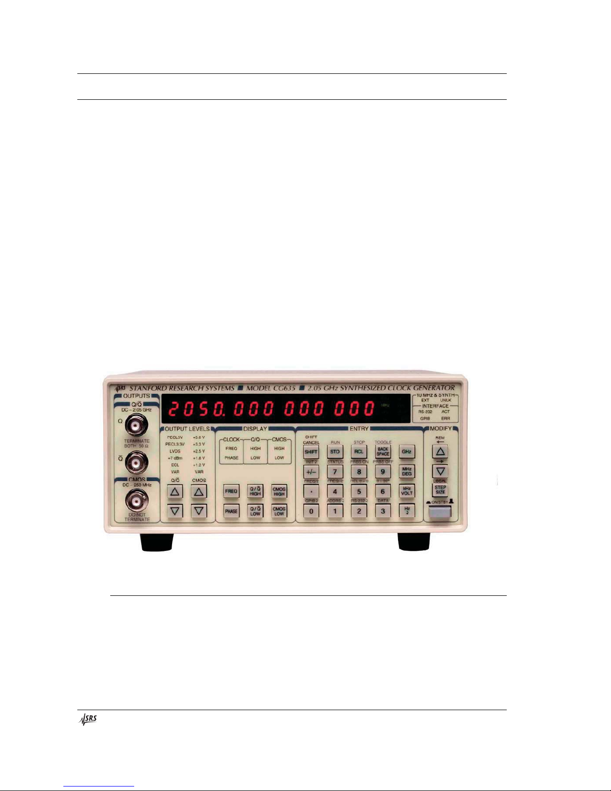
CG635 Synthesized Clock Generator
Display
The DISPLAY section allows the user to select which values are reported in the main
front panel display. The LEDs in the display section indicate what is currently being
displayed or edited. The meaning of the LEDs and keys are summarized in Table 3.
Table 3: DISPLAY Section Keys
Label Value Shown in Main Display When Pressed
FREQ Current frequency
PHASE Current phase
Q / Q¯ HIGH Voltage for a Q / Q¯ logic high state
Q / Q¯ LOW Voltage for a Q / Q¯ logiclowstate
CMOS HIGH Voltage for a CMOS logic high state
CMOS LOW Voltage for a CMOS logic low state
The keys are used to change the main display to the indicated item. Pressing ‘FREQ’, for
example, will cause the CG635 to display the current frequency. The FREQ LED will
turn on, indicating that the current display is frequency.
Entry
Numeric Entry
The ENTRY section is used to modify the current settings of the CG635. In most cases,
the currently displayed item can be changed by entering a new value with the numeric
keys, and pressing an appropriate units key to complete the entry. For example, if the
frequency is currently being displayed, pressing the keys ‘1’, ‘MHz’, sequentially will
change the frequency to 1 MHz. Similarly, if the CMOS HIGH voltage is displayed,
pressing the keys ‘2’, ‘.’, ‘1’, ‘VOLT’ will set the CMOS logic high voltage to 2.1 VDC.
Store and Recall Settings
The ‘STO’ and ‘RCL’ keys are for storing and recalling instrument settings, respectively.
The instrument saves the frequency, phase, Q / Q¯ and CMOS output levels, all the
associated step sizes, the run/stop state, the PRBS state, and the current display. Up to ten
different instrument settings may be stored in the locations 0 to 9. To save the current
settings to location 5, press the keys ‘STO’, ‘5’, ‘Hz’, sequentially. To recall instrument
settings from location 5, press the keys ‘RCL’, ‘5’, ‘Hz’ sequentially.
Secondary Functions
Many of the keys have secondary functions associated with them. The names of these
functions are printed above the key. The ‘4’ key, for example, has FREQx2 above it. The
meaning of the secondary functions is summarized in Table 4.
Table 4: Secondary Functions
Label Function Description
RUN Enables the output. Drives the output at the current frequency.
STOP Stops the output. Forces the output to a logic low state.