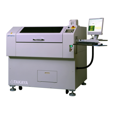
TAKAYA APT-9411 Series Manual

IC open test
IC open test IC open test
IC open test s
ss
system
ystemystem
ystem
CS
CSCS
CS-
--
-9
99
95
55
500
0000
00
Operator’s Guide
Operator’s GuideOperator’s Guide
Operator’s Guide
TAKAYA


i
Preface
The IC Open test system CS-9500, one of exclusive options for Takaya Fixtureless Tester PT-9411
Series, enables to detect unsoldered IC leads of QFP, SOJ, so on while contacting the independently
moving sensor probes on the IC’s package.
This Operator’s guide covers the functions, programming, operation, maintenance and specifications
of the IC Open Test system CS-9500. Read this Operator’s guide thoroughly before using this option
in order to understand the features and keep this Operator’s guide readily available for reference.
In addition, this Operator’s guide also explains you on the Underside IC Open Test system CSU-9500
at the end of this Operator’s guide.
If you have any question or thoughts you would like to share with us - we would like to hear from you.
(NOTE)
(1) This Operator’s guide is based on the PT-9411 Series software Ver1.3-3.
(2) No portion of the contents of this publication may be reproduced or transmitted in any form or by
any means without the express written permission of T K Y Corporation.
(3) The design of the product is under constant review and whilst every effort is made to keep this
Operator’s guide up to date, the rights is reserved to change specifications and equipment at any
time without prior notice.

ii
Introduction
Operation keys and SW
(1) ll operation keys on the keyboard are begirt by [ ] mark such like [ Enter ] key, [ SP ] key.
(2) ll SWs on the operation panel are also displayed like [ TEST START ].
(3) If some plural keys need to be depressed in order, they are combined with “ > “.
For example, in case of [ A ] > [ 3 ] key, first depress [ A ] key then [ 3 ] key.
(4) If some plural keys need to be depressed at a time, they are combined with “ + “.
For example, in case of [ Ctrl ] + [ Y ] key, depress [ Ctrl ] key and [ Y ] key at a time.
Safety sy bols
The Operator’s guide uses the following headings to display important safety information and so on.
Strict adherence to the instruction next to these heading is required at all times.
Symbol Explanation
Calls attention to a procedure, practice, or condition that could possibly cause
serious accident or death.
Calls attention to a procedure, practice, or condition that could possibly cause
bodily injury or damage to the product.
Calls attention to a procedure, practice, or condition that could possibly damage
to the product.
Calls attention to general instruction.
Failing to follow this could loss of data stored on disks, cause possibly misjudge
the unit under test, or damage to the product.
Calls attention to especially key operation.
Calls attention to “One-point advice” which should be useful when you are at a
loss to operate the products.

iii
Safety precautions
Since this section summarizes the precautions to be observed to operate the IC Open Test system
CS-9500 in safety, be sure to read it before operation.
All instructions below are very i portant! Do not atte pt to install and/or use
the product unless you could understand any of the .
1. Never modify or repair any part of the product by yourself. Otherwise it may possibly cause an
electric shock or other bodily accident.
2. For safety reason, it is recommended that only one person operate the product. If not, the product
may cause an unthought of action and a serious accident as the result.
3. Never attempt to put a part of your body in the working area of the product. Otherwise it may
possibly cause a serious accident.
4. While using the product, be sure to close the safe cover of the tester. Otherwise it may possibly
cause an electric shock or other bodily accident.
5. Once some smoke or bad smell came from the product, it may possibly cause a burning or electric
shock and is very dangerous. In such case happened, switch the power off and stop operating the
product on the spot, then consult to our local distributor for the solution. Do not use the product
until safe operation can be verified by service-trained personnel.
6. Once some liquid or foreign material was put in the product, it may possibly cause a burning or
electric shock and is very dangerous. In such case happened, unplug the product and stop your
operation on the spot, then consult to our local distributor for the solution. Do not use the product
until safe operation can be verified by service-trained personnel.
7. Once you felt something strange during the operation (i.e. noise, smell, malfunction, etc.), switch
the power off, unplug the product and stop your operation on the spot, then consult to our local
distributor for the solution. Do not use the product until safe operation can be verified by
service-trained personnel.
8. The product power must be OFF and unplugged when the product is serviced for maintenance or
cleaning. Needless to say, the service must be made by service trained personnel only who are
familiar with electronic circuitry and understand the hazard involved.
9. The product power must be OFF and unplugged before replacing or maintenance any part of this
option.
10. The manufacturer has no responsibility for such defect resulting from misuse or unauthorized
modification by user, as well as operation outside of the environmental specifications for the
product.
- 1 -
§
§§
§1 General
This section provides fundamental information on the IC Open Test system CS-9500.
Outline
With this optional system built-in, the Takaya PT-9411CE Series (hereafter “Tester”) enables to detect
unsoldered IC leads of QFP, SOJ, so on while contacting the independently moving sensor probes on
the IC’s package. unique spring-embedded sensor probe (hereafter “Sensor probe”) contacts the IC
leads directly in place of the probe, so that the test is unlikely to be falsely judged due to possible
contact error. In addition, the test program is easily and automatically created in a very short period of
time.
CS-9500 Hardware
(1) IC Open measuring PCB (T K Y TVX-11)
(2) ntenna drive unit and Sensor probe (Each one at Left/Right)
Hardware location
The hardware is installed in the tester as shown in Fig.1 below.
[Fig.1] Tester appearance
Measuring principle
The measurement principle is outlined below.
[Fig.2] Measuring principle
s Fig.2 introduce, the sensor probe is supposed to contact directly on the IC package under test
while impressing C measurement signal between an individual IC’s lead and the GND point on the
PC board. This sensor probe consists of a special antenna that can receive a signal radiated from the
lead frame inside the IC through its mold package. If some IC’s leads were improperly soldered
otherwise open, the signal level becomes small so that their failure can be detected accordingly.
ntenna drive unit & Sensor probe
IC open measuring PCB

- 2 -
Antenna drive unit & Sensor probe installation
The antenna drive unit that includes the sensor probe is installed on the Z2 axis and the Z3 axis.
Contact position of Sensor probe and probe
s shown in Fig.3 below, the sensor probe which is equipped with a round sensor plate (diameter
φ5mm) on the top steps on IC package where is nearby each IC lead to be measured. So their
stepping position shifts sequentially according to the testing order.
[Fig.3] Sensor probe’s contact position
Meanwhile, the contact position for the probes which impress the necessary measurement signal
should be properly selected depends on the IC solder pad.
Large solder pad
When there is enough space on the IC solder pad and a few possibilities that any probe may
interfere with the IC lead, it should contact on the IC solder pad directly.
S all solder pad
When there is less space on the IC solder pad, in other words there is a risk for the probe to
interfere with the IC lead, otherwise when the objective IC is PLCC-type which has no IC solder pad,
the probe should contact any other point where is connected with the objective IC solder pad on the
same circuit pattern.
[Fig.4] Probe’s contact position
In addition, two GND points where to contact by another probe should be available on the left-hands
and the right-hand corners on your PC board. If the GND point was set incorrectly, some of IC open
test steps would not be created. (In this case, the VF measurement steps is created instead)
Reference Value for PASS/FAIL Judgment
The reference value for the IC open test is also learned from a good sample PC boards automatically
as usually done to program the component steps.

- 3 -
Progra ing IC Open Steps
The tester allows easy programming of IC Open test as well. The user can use a CCD camera to
directly input the XY coordinates where the sensor probe contacts or outsource the creation of test
program to C D data converters. Inputting the XY coordinates of all four corners on the IC package as
well as the number of the IC leads, the tester can automatically create the XY coordinates for the
sensor probes to contact.
Measura le ICs and conditions
1. IC outward dimension is over 6mm each side (QFP, SOP, PLCC, LCC, MSP, so on)
2. IC mold thickness is less than 2.5mm from the lead frame. (It depends on the material and the
frame area)
3. The probe is more than 2.8mm away from the sensor probe
[Fig.5]
Unmeasura le ICs and conditions
1. Unmeasurable ICs
• SIP and such ICs that has no or a very small lead frame inside the IC’s package
• ICs which mold thickness is more than 2.5mm from the lead frame
• ICs in which shield plate or heat sink is installed over the lead frame
2. Unmeasurable conditions
• GND line and Vcc line
• IC’s lead with very low impedance of less than 20 ohm (equivalent to approx. 0.9µF or more in
Capacitance) against GND line or Vcc line.
[Fig.6] Unmeasurable ICs and conditions
The IC open test of two adjacent IC leads on the same line is possible only when they
got fail at the same time.
ny breaking of the lead wire inside the ICs, any miss-orientation, or any miss-mount
cannot be detected.
There may be other cases that are unmeasurable due to the wiring (and mounting)
condition on the boards or type of the ICs being tested.
GND
Vcc
Low impedance
Less 20 Ω
Low impedance
Less 20 Ω
△
△△
△ Measurable when both two were fail at a time
✖
Unmeasurable
IC lead
Sensor probe
Probe

- 4 -
Test speed
The test speed depends largely on travel distance of the test probes and the IC lead pitches. Let’s say
for instance that we test a QFP with 0.65mm pitch while directly contacting the IC lead pads. In this
case, we can estimate max. 0.10 - 0.15 sec./point approximately.
Test area (Sensor probe’s oving area)
PT-9411CE : W540 x D460 x H15 (mm)
PT-9411SL : W635 x D609 x H15 (mm)
[Fig.7] Sensor probe’s moving area
Movable area of the sensor probe is equal with the maximum PC board size to be set
on the tester.
Other specifications
Measurement signal C140mVrms (f=5KHz,10KHz)
Up/Down mechanism Stepping servo motor & timing belt
Lowest position set Programmable for 0-15mm per step
Maximum sensor stroke pprox. 6mm
Initial spring pressure pprox. 124g
Spring pressure under 1/2 stroke pprox. 409g
Spring pressure under full stroke pprox. 694g
Spring lifetime More than 10 million strokes (at 1/2 stroke)
Front side
H15mm
W635mm
D609mm
Front side
H15mm
W540mm
D460mm

- 5 -
§
§§
§2 Test Data programming
This section describes the procedure for preparing a program of the IC open test.
Initial setup
The sensor probe to probe offset must be adjusted carefully by the following operation. The tester
requires this initial setup by the user at the time of first using the IC open test system and each time
the sensor probe (also the sensor probe base) is replaced by new one.
1. Use your mouse to click Option Mode. (Tool > Mode Setting > Option Mode)
2. The Option Mode window is displayed on the screen.
3. Choose IC Open from the menu list.
4. Let’s say for example that you need to adjust the sensor probe to probe offset on rm #3. In this
instance, double click on the coordinates at the 3X box.
5. It displays the pop-up message “Press [TEST ST RT] SW” on the screen.
6. Press [TEST ST RT] SW on the operation panel.
7. The JOG window is displayed on the screen.

- 6 -
Use the keypad arrow keys to drive the 3Z arm and set the probe on any reference point on the
horizontal line or any Via hole on your PC board. fter the position was determined, press [Enter]
SW to enter the X,Y coordinates.
8. The next window appears on the screen. Press [TEST ST RT] SW on the operation panel.
9. The JOG window is displayed on the screen.
10. Use the keypad arrow keys to drive the 3Z arm and set the front side of the sensor plate for the
X,Y coordinates assigned by Probe (3Z). fter the position was determined, press [Enter] SW to
enter the X,Y coordinates.

- 7 -
11. The sensor probe moves to the Machine reference point automatically while displaying the
following window on the screen.
12. Ensure that the sensor probe is at the center of the Machine reference point and click on [OK]
button. If the sensor probe has some deviations, click on [Cancel] button and repeat the same
operation from Process 4.
13. The JOG window is displayed on the screen.
Now the sensor probe to probe offset on rm #2 requires to be adjusted.
14. Use the keypad arrow keys to drive the 2Z arm and set the probe on any reference point on the
horizontal line or any Via hole on your PC board. fter the position was determined, press [Enter]
SW to enter the X,Y coordinates.
15. The next window is displayed on the screen. Press [TEST ST RT] SW on the operation panel.

- 8 -
16. The JOG window is displayed on the screen.
17. Use the keypad arrow keys to drive the 2Z arm and set the front side of the sensor plate for the
X,Y coordinates assigned by Probe (2Z). fter the position was determined, press [Enter] SW to
enter the X,Y coordinates.
18. The sensor probe moves to the Machine reference point automatically.
19. It displays the following window on the screen.
20. Ensure that the sensor probe is at the center of the Machine reference point and click on [OK]
button. Then the display goes back to the Option Mode window. If the sensor probe has some
deviations, click on [Cancel] button and repeat the same operation from Process 13.
21. Click on [OK] button to quit the Option Mode window.
22. ll that you need to do for Initial set was finished.

- 9 -
Auto atic generation of IC open test
The tester offers two options to manage the XY coordinates in your test programs. One method is
so-called “Teaching syste ” that utilizes the solder lands and the electrodes to test the UUT. nother
one is so-called “Point syste ” that utilizes any test point from each circuit patterns. Those
coordinate management systems are user-selectable on the Coordinates Management window in
Data mode.
Prior to start progra ing a test data, ensure that the box “Use Auxiliary
Reference Point(s)” on the Auxiliary Reference Point(s) window (Tool > Mode
setting > Data Mode) is selected.
Practical operation in Teaching system
The IC open test is automatically created by using the uto. Generation function available on Step
Edit/List menu. (Tool > Step Edit/Step List > uto. Generation)
(Ex.1) How to progra the IC open test for the following IC
Preparation
Coordinates Management system (Tool > Mode setting > Data Mode) should be specified to Teaching
system in advance.
1)
Select either Step Edit or Step List from Menubar.
2)
It displays the Step Edit window or the Step List window.

- 10 -
Step List window
3)
Select uto. Generation function from the Menubar. (Tool > uto. Generation)
4)
It displays the pop-up message “Use board ref. point and aux. ref. point for alignment?” on the
screen.
5)
Click on [Yes] button.
6)
It displays the pop-up message “Press [TEST ST RT] SW” on the screen.
7)
Press [TEST ST RT] SW on the operation panel.
8)
lign the inclination and/scale of the PC board by manually centering the camera target on the
board reference point and auxiliary reference point(s) or automatically using the image processing
unit (option).
9)
It displays the uto. Generation window.
Type “Parts name’, ‘Comment’ and ‘location’ from the keyboard. Then click on [Next] button.
10)
It proceeds to the next window where you can specify a preferable generation function.
Fill ‘IC automatic generation’ radio button and click on [Next] button.

- 11 -
11)
It proceeds to the next window where you can specify a preferable generation style.
Fill ‘IC open test only’ radio button and click on [Next] button.
12)
It proceeds to the next window where you can specify a preferable generation pitch.
Fill ‘Regular pitch’ radio button and click on [Next] button.
13)
It proceeds to the next window where you can specify information on the IC lead number.
Type “8, 9, 16, 17, 24, 25, 32” from the keyboard and click on [Next] button.
14)
It proceeds to the next window where you can specify GND pin number.
Type “7” from the keyboard and click on [Next] button.

- 12 -
15)
It proceeds to the next window where you can input the XY coordinates for the IC leads you
specified at Process #13.
Drive the camera to enter the X,Y coordinates of the IC lead #1, 8, 9, 16, 17, 24, 25 and 32 in
order and click on [OK] button.
Probing position
Ideally all probing position should be on the IC land, not directly on any IC leads.
Otherwise it may possibly mislead the judgment, because the open circuit at IC lead
can be touched by the probing pressure.
16)
It proceeds to the next window where you can input the XY coordinates for the two GND points
that should set at the lower left and the upper right of the IC which is under way.
Drive the camera to enter the X,Y coordinates at the two GND points and click on [OK] button.
17)
It proceeds to the next window where you can input the X,Y coordinates at each corners of the IC
package.
✖
Upper right area
Front side
Lower left area
✖

- 13 -
Drive the camera to enter the X,Y coordinates at the four corners of the IC package and click on
[OK] button.
18)
The IC Open test steps are generated on the list automatically.
In case that the GND points for IC open test were set up incorrectly, otherwise
when probe access was li ited, IC open test steps ay be not generated so that
they are converted to nor al VF easure ent steps (‘Pin to GND’)
auto atically.
The Auto. Generation window is also displayed by substituting “=” ark in
Value colu n and hitting [Enter] key on the Step Edit enu and the Step List
enu.
After IC open steps were generated, ‘ICOP’ is substituted in Aux. colu n of their
test steps.
Lower left corner
Lower right corner
Upper left corner
Front side
Upper right corner

- 14 -
Practical operation in Point system
The IC open test is automatically created by using the uto. Generation function available on Step
Edit/List menu. (Tool > Step Edit/Step List > uto. Generation)
Undermentioned is a practical example to make IC Open test steps.
(Ex.2) How to progra test steps only for the IC below
Preparation
Coordinates Management system (Tool > Mode setting > Data Mode) should be specified to Point
system in advance.
1)
Select either Step Edit or Step List from Menubar.
2)
It displays the Step Edit window or the Step List window.
Step List menu
3)
Select uto. Generation function from the Menubar. (Tool > uto. Generation)
Other manuals for APT-9411 Series
3
Table of contents
Other TAKAYA Test Equipment manuals