Operating I
nstructions-7
A15
GENERAL OPERATING INFORMATION
Signal Connection
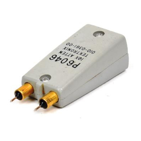
In general, probes offer
the
most
convenient means of
connecting a signal
to
the
input
of
the
7A15. Tektronix
probes are shielded
to
prevent pickup
of
electrostatic inter-
ference. A
lOX
attenuator
probe
offers a high
input
im-
pedance and allows
the
circuit
under
test
to
operate very
close
to
normal operating conditions. However, a
lOX
probe also
attenuates
the
input
signal
ten
times.
In
high-frequency applications requiring maximum over-
all bandwidth, use a coaxial cable terminated
at
both
ends
in
the
characteristic impedance
of
the
cable.
To
maintain
the
high-frequency characteristics of
the
applied signal, use
high-quality low-loss cable. Resistive coaxial
attenuators
can be used
to
minimize reflections
if
the
applied signal has
suitable amplitude.
High-level low-frequency signals can be connected direc-
tly to
the
7A15
INPUT
connector
with short unshielded
leads using a
BNC
to
Banana Jack Adapter. This
method
works best for signals below
about
one kilohertz and deflec·
tion factors above
one
volt/division. When this
method
is
used, establish a
common
ground between
the
7A15 and
the
equipment
under
test
(common ground provided by
line cords
is
usually inadequate).
Attempt
to
position
the
leads away from any source
of
interference
to
avoid errors
in
the
display.
If
interference
is
excessive with unshielded
leads, use a coaxial cable
or
a probe.
I
nput
Coupling
The AC-GND-DC lever switch allows a choice of
input
coupling. The
type
of
display desired determines
the
mode
of
input
coupling used.
The
DC
position can be used for
most
applications. However,
if
the
DC
component
of
the
signal
is
much larger
than
the
AC
component,
the
AC
position will probably provide a
better
display.
DC
coupling
should be used
to
display
AC
signals below
about
2 hertz
and square waves containing low-frequency
components,
as
they
will be
attenuated
in
the
AC
position.
In
the
AC
position,
the
DC
component
is
blocked by a
capacitor
in
the
input
circuit.
The
low-frequency response
in
the
AC
position
is
about
2 hertz
(-3
dB
point). There-
fore, some low-frequency
attenuation
can be expected near
this frequency limit. Distortion will also appear
in
square
waves which have low-frequency components.
The
GND position provides a ground reference
at
the
amplifier input.
The
signal applied
to
the
INPUT
connector
is
presented with a
one
megohm load, while
the
amplifier
input
is
grounded. This eliminates
the
need
to
externally
ground
the
INPUT
to
establish a
DC
ground reference.
2-4
The
GND position
is
also used
to
pre-charge
the
coupling
capacitor
to
the
average level
of
the
signal applied
to
the
INPUT connector.
The
pre-charge network allows
the
input
coupling capacitor
to
charge
to
the
DC
source voltage level
when
the
COUPLING switch
is
set
to
GND.
The
procedure for using this feature
is
as follows:
1. Before connecting
the
signal containing a
DC
com-
ponent
to
the
7A15 INPUT, set
the
COUPLING switch
to
GND. Then
connect
the
signal
to
the
INPUT connector.
2. Allow
about
two
seconds for
the
coupling capacitor
to
charge.
3. Reset
the
COUPLING switch
to
AC.
The
trace
(display) will remain on
the
screen and
the
AC
component
of
the
signal can be measured
in
the
normal manner.
Deflection
Factor
The
amount
of
vertical deflection produced by a signal
is
determined by
the
signal amplitude,
the
attenuation
factor
of
the
probe
(if any),
the
setting
of
the
VOLTS/DIV switch
and
the
setting
of
the
VAR IABLE control (if control
is
in
the
outward position).
The
calibrated deflection factors
in-
dicated by
the
VOLTS/DIV switch apply only when
the
VARIABLE control
is
in
the
inward (CAL
IN)
position.
The
VAR IABLE control provides uncalibrated vertical
deflection between
the
calibrated settings
of
the
VOL
TS/
DIV switch, and
extends
the
maximum deflection factor
to
at
least 12.5 volts/division.
The
GAIN
control,
a front-panel screwdriver adjustment,
sets
the
gain
of
the
7A15
in
the
10 mV/div position
of
the
VOLTS/DIV switch.
The
gain calibration
of
the
unit
should
be checked for accuracy prior
to
making critical measure-
ments, using either
the
oscilloscope calibrator
output
or
a
standard amplitude calibrator. If
adjustment
is
necessary,
the
GAIN should be adjusted with
the
VOLTS/DIV switch
set
to
10 mY.
Variable Balance
To
check
and/or
adjust
the
VAR BAL, proceed as fol-
lows:
1.
Set
the
COUPLING
to
GND and adjust
the
time-base
controls
for
a free-running trace.
2. Press and release
the
VAR IABLE control
to
its out-
ward position.
®
