Operating Instructions — Type Z
Fig. 2-2. Left rear side view of the Z Unit showing location of the
AMP DC BAL adjustment.
impedances. Unterminated connections result in reflections
in the cables and cause distortion of the displayed wave
forms.
When input signal connections are made, consider the
effect of loading upon the signal source due to the input
circuit of the Z Unit. The input resistance of the Z Unit is 1
megohm which is generally adequate to limit low-frequency
loading to a negligible value. At high frequencies, however,
the input capacitance of the Z Unit and the distributed
capacitance of cables become important. Capacitive load
ing at high frequencies may be sufficient to adversely
affect both the displayed waveform and the operation of
the signal source. Both capacitive and resistive loading
can usually be limited to negligible values through use
of attenuator probes.
Use of Probes
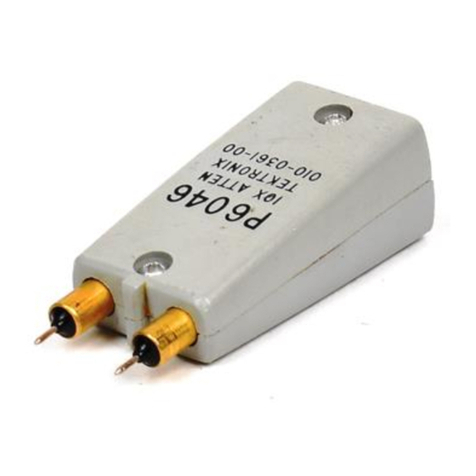
Attenuator probes reduce loading of the signal source.
However, in addition to providing isolation of the oscillo
scope from the signal source, an attenuator probe also de
creases the amplitude of the displayed waveform by the
attenuation factor of the probe. When making amplitude
measurements with an attenuator probe, be sure to multi
ply the observed amplitude by the attenuation of the probe.
(Additional information concerning probe attenuation will
be found under Differential Preamplifier Operation and At
tenuator Test Point portions of this section of the manual.)
An adjustable capacitor in the probe body compensates
for variations in input capacitance from one instrument to
another. To assure the accuracy of pulse and transient meas
urements, this adjustment should be checked frequently.
To make this adjustment, set the oscilloscope calibrator
controls for a calibrator output signal of suitable amplitude.
Touch the probe tip to the calibrator-output connector and
adjust the oscilloscope controls to display several cycles
of the waveform. If the probe cable is connected to the
A input connector on the Z Unit, adjust the probe capacitor
for flat tops on the calibrator square wave. If it is connected
to the B input connector, adjust for a flat bottom on the
square wave.
Conventional Preamplifier Operation
When the Z Unit is used for conventional preamplifier
operation, the Mode switch should be placed in either
the A ONLY or the —B ONLY position. Input signals should
then be connected to the corresponding input connector.
Operation of the unit in the two positions is essentially the
same except that signals applied to the B input connector
are inverted on the display. Positive voltages produce an
upward deflection when applied to the A input connector
and a downward deflection when applied to the B input
connector (see Fig. 2-3).
Fig. 2-3. W aveform s applied to the A Input connector produce an
upright display, while waveforms applied to the B Input are in
verted.
The amount of vertical deflection produced by a signal
is determined by the settings of the VAR. ATTEN. control
and the VOLTS/CM switch. Calibrated deflection factors
indicated by the settings of the VOLTS/CM switch apply
only when the VAR. ATTEN. control is set fully clockwise.
Serious errors in display measurements may result if the
setting of this control is inadvertently moved away from
the fully clockwise position.
The range of the VAR. ATTEN. control is approximately
2.5 to 1 to provide continuously variable (uncalibrated)
vertical-deflection factors between calibrated settings of
the VOLTS/CM switches.
Voltage measurements may be made directly from the
oscilloscope screen by noting the deflection factor on the
appropriate VOLTS/CM switch dial, and the amount of
deflection on the screen. Then multiply the deflection on
the screen by the setting of the VOLTS/CM switch and the
attenuation factor, if any, of the probe.
Placing the AC-DC switch in the AC position inserts a dc
blocking capacitor in series with the input circuit. In the
AC position, the input time constant is 0.1 second and the
low-frequency response is —3 db at 2 cps. Thus some
attenuation exists even at 0 cps. Because the input dc
signal may be suppressed by means of the calibrated com
parison voltage feature, there are few occasions where the
ac-coupling mode will be needed. Two principle occasions
are: (1) When it is desired to get a quick look at the ac
component of a signal which has a large dc component
and (2) where there is a difference in dc levels of the two
signals to be observed during differential mode of operation.
The tolerances of the input circuit time constants (at
—3 db frequency) are nominally =h2%. When tighter
®T 2-3
http //manoman.sqhill.com
