manuals.online logo
Brands
  1. Home
  2. •
  3. Brands
  4. •
  5. Tektronix
  6. •
  7. Amplifier
  8. •
  9. Tektronix 7A22 User manual

Tektronix 7A22 User manual

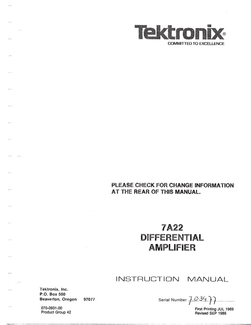
Tektronix-
COMMITTED TO EXCELLENCE
7A22
DIFFERENTIAL
AMPLIFIER
INSTRUCTION MANUAL
Tektronix, Inc.
P.O. Box 500
Beaverton, Oregon 97077
070-0931-00
Product Group 42 First Printing JUL 1969
Revised SEP 1986
Copyright ?1969 Tektronix, Inc. All rights reserved.
Contents of this publication may not be reproduced in any
form without the written permission of Tektronix. Inc.
Products of Tektronix. Inc. and its subsidiaries are covered
by U.S. and foreign patents and/or pending patents.
TEKTRONIX. TEK. SCOPE-MOBILE, and are
registered trademarks of Tektronix. Inc. TELEQUIPMENT
is aregistered trademark of Tektronix U.K. Limited.
Printed in U.S. A. Specification and price change privileges
are reserved.
INSTRUMENT SERIAL NUMBERS
Each instrument has aserial number on apanel Insert, tag,
or stamped on the chassis. The first number or letter
designates the country of manufacture. The last five digits
of the serial number are assigned sequentially and are
unique to each instrument. Those manufactured in the
United States have six unique digits. The country of
manufacture is identified as follows:
BOOOOOO Tektronix. Inc., Beaverton. Oregon, USA
100000 Tektronix Guernsey, Ltd.. Chanr>el Islands
200000 Tektronix United Kingdom, Ltd.. London
300000 Sony/Tektronix. Japan
700000 Tektronix Holland, NV, Heerenveen,
The Netherlands
7A22
TABLE OF CONTENTS
Page
Section 1SPECIFICATION
Introduction 1-1
Electrical Characteristics 1-1
Deflection Factor 1-1
Gain 1-1
Differential Dynamic Range .1-1
DC Offset 1-1
Frequency Response 1-1
Bandwidth Limit 1-1
Recovery Time 1-1
Common-Mode Signal Range .1-1
Common-Mode Rejection Ratio . . 1-1
Maximum input Voltage 1-3
Input Rand C1-3
Maximum Input Gate Current 1-3
Variable Balance 1-3
Step Attenuator DC Balance 1-3
Displayed Noise (Tangentially
Measured) 1-3
DC Drift 1-3
Isolation Between 4and
Inputs 1-3
Environmental Characteristics 1-3
Altitude 1-3
Transportation 1-3
Physical Characteristics 1-3
Finish 1-3
Dimensions 1-3
Weight ..... 1-3
Section 2OPERATING INSTRUCTIONS
Introduction 2-1
Front Panel Controls and Connectors .2-1
Operating Instructions ..2-2
Rrst Time Operation 2-2
General Operating Information 2-4
Trace Drift 2-4
Input Gate Current 2-4
Page
Section 2OPERATING INSTRUCTIONS
(COnt)
Voltage Measurement 2-4
Signal Input Connectors 2-4
High Input ImpedarKe 2-5
Display Polarity 2-5
Deflection Factor 2-5
Bandwidth Selection 2-5
Voltage Comparison Measurements .2-10
Differential Operation 2-10
DC Offset Operation 2-11
Input Overdrive Indicator 2-12
Readout 2-12
Trace Identify 2-13
\WAfIMING
The remaining prytion of this TaUe of Contents lists the
servicing instructions. These servicing instructions are for
use by qualified personnel only. To avoid electrical shock,
do not perform any servicing other than that called out in the
operating instructions untess qualified to do so.
Section 3CIRCUIT DESCRIPTION
Introduction 3-1
Block Diagram Description 3-1
Input Coupling 3-1
Input Attenuators .3-1
Preamp 3-1
LF 3dBPoint 3-1
Output Amplifier 3-2
HF-3dB Point 3-2
General Information 3-2
Feedback Amplifiers 3-2
Differential Configuration 3-3
Detailed Circuit Description .3-3
Input Coupling 3-3
Input Attenuators .3-4
REV SEP 1981 i
7A22
TABLE OF CONTENTS (cont)
SECTION 3CIRCUIT DESCRIPTION (cont) Pag*
Gate Current Compensation .3*4
Input Amplifier 3-4
X15 Preamp 3-4
DC Balance 3-4
Floating Power Supply ... 3-5
Common-Mode Rejection .3-5
Cross Neutralization 3-6
Input Overdrive Protection 3-7
DC Offset 3-7
Offset Generator 3-7
Input Overdrive indicator .3-8
LF-3 dB Point Selector .3-9
Output Amplifier 3-9
Gain Switching Amplifier .3-9
Variable Output stage .... 3-11
Signal Output Amplifier ..3-11
Trigger Output Amplifier ..3-11
IndicatorOscilloscopeReadout 3-11
Probe Sensing 3-11
Trace Identify 3-11
SECTION 4MAINTENANCE
Introduction 4-1
Preventive Maintenance 4-1
General 4-1
Cleaning Front Panel 4-1
Cleaning Interior 4-1
Visual Inspection 4-1
Transistor Checks 4-1
Calibration 4-i
Corrective Maintenance 4-1
General 4-1
Obtaining Replacement Parts 4-2
SECTION 4MAINTENANCE (cont) Page
Special Parts 4-2
Soldering Techniques 4-2
Component Replacement
Information 4-3
Troubleshooting 4-5
Introduction 4-5
Indicator Oscilloscope 4-5
Operating Procedure and
Control Settings 4-5
Trouble Symptoms 4-5
Visual Inspection 4-5
Calibration Check 4-5
Detailed Troubleshooting 4-5
Test Equipment Recommended 4-6
DC Balance Check 4-6
Troubleshooting by Direct
Replacement 4-6
Components Checks 4-6
Transistors 4-6
Diodes 4-8
Resistors 4-8
Capacitors 4-9
Repackaging for Shipment .... 4-9
SECTION 5PERFORMANCE CHECK/
CALIBRATION PROCEDURE
Introduction 5-1
Test Equipment Required 5-1
General 5-1
Short Form Procedure 5-2
Performance Check/Calibration
Procedure 5-3
General 5-3
Preliminary Procedure 5-3
II REV C. MAR 1979
TABLE OF CONTENTS (cont)
7A22
SECTION SPERFORMANCE CHECK/
CALIBRATION PROCEDURE
(coni) Page
Check or Adjust 5-4
AC Step Alien Balance ... 5-4
Variable Balance 5-4
Coarse DC Balance 5-4
+Gate Current Zero 5-5
Gate Current Zero 5-5
GAIN 5-5
VARIABLE Control Ratio . . 5-5
VOLTS/OIV Gain Switching 5-5
Isolation between and -
Inputs 5-6
Total DC Offset Range . . .5-6
C241 -t-Cross Neutralization 5-7
C141 -Cross Neutralization 5-7
C115 X1 -Hnput Atten Time
Constant 5-7
C215 X1 -Input Atten Time
Constant 5-7
Input Atten Accuracy .... 5-8
Input Atten Differential
Balance 5-B
Hnput Atten Series
Conpensation 5-9
-Input Atten Compensation 5*9
Input Atten Shunt
Compensation 5-tO
HF-3dBPoint 5-11
SECTION SPERFORMANCE CHECK/
CALIBRATION PROCEDURE
(cont) Page
LF -3 dB Point 5-11
CMRR 5-12
Input Overdrive Indicator .5-12
Differential Dynamic Range 5-13
Overall Noise Level
(Measured Tangentially) . . 5-13
Overdrive Recovery Time .5-14
SECTION 6ELECTRICAL PARTS LIST
Abbreviations and Symbols
Parts Ordering Information
Index of Electrical Parts List
Electrical Parts List
SECTION 7DIAGRAMS AND MECHANICAL
PARTS ILLUSTRATIONS
Diagrams
Mechanical Parts Illustrations
SECTION 8MECHANICAL PARTS LIST
Mechanical Parts List Information
Index of Mechanical Parts
Illustrations
Mechanical Parts List
Accessories
Abbreviations and symbols used in this manual are based on or
taken directly from IEEE Standard 260 "Standard Symbols for
Units", MIL STD-12B and other standards of the electronics
industry. Change information, if any. is located at the rear of this
manual.
Hi
REV B. MAR 1979
fig. I'l. Type 7Ai7 (Hff*r«n(tcl AiaplHItr.
Typ* 7A22
Typ* 7A22
SECTION 1
SPECIFICATION
Change informotion, if any, affecting this section will be found at the
rear of the manual.
Introductior)
Th« Type 7A72 Vartical Plug-in is aDC coupled differ-
enliol omplilier with excellent common-mode rejection chor-
octeristics ond high goin for low level applications.
The DC Offset copobility of the Type 7A22 ollows the
display of the very smoll low-frequency signals containing
alorge DC component, ot deflection foctors r>ol possible with
AC coupling. The verticol deflection factor ronge of the
Type 7A72 is from lOfiV to lOV. The high and low fre-
quency -3dB points con be selected at the front panel,
to set the bandwidth of the instrument. Thus, for low fre-
queiKy applications the sigrtol lo-noise ratio con be improved
by restricting the bandwidth of the Type 7A23. The bond-
width selection ond excellent drift-with-time charocteristics
provide measurement copobilities in the biomedical, trans-
ducer, orsd other areas which require stable, low deflection
factor, low noise measurements.
The Type 7A22 is desigrted for use in Tektronix 7000 Series
oscilloscopes.
The electrical choracteristics described in this section ore
valid over the stated environmental range for instruments
calibrated at on ambient lemperolure of -f20*C to -|-30*C
ond after aSminute wormup unless otherwise rtoted.
aeCTRICAL CHARACTERISTICS
Chorocleristic Performonce Requirements
Deflection Foctor
(VOLTS/DIVl
Gain Rotio Accurocy Within 3% with GAIN odjusted at
1mV/div
VAR (CAL IN) Range Continuously variable; extends de-
flection foctor to at least 25V/div
GAIN Permits odjustment of deflection
foctor ot 1mV/DIV for oil moin-
fromes
Differential Signal Range
(DC OFFSET not used)
lO^V/Div to
lOmV/Div At least -±1 V
20mV/Div to
0.1 V/Div At leost d;)0V
0.3V/Div to
1V/Div At leost d;100V
2V/Div to
lOV/Dfv At least dIOOOV
DC OFFSET
COARSE Range from
Electrical Zero
lOf^V/Div to
lOmV/Div At least t-l Vto -~l V
20 mV to 0.1
V/Div At least -f 10V to -10V
0.2 Vto 1V/Div At least 4100 Vto -100 V
2V to 10 V/Div At least 4IOOOV to -1000V
Frequency Response (6
div Referersce)
Overall Frequertcy
Response DC (Direct)
Coupled Input
DC to within 10% of 1MHz ot
-3dB
AC (Copacitive) Cou-
pled Input lower
Bofsdwidth Freqi>er>cy
2Hz or less
BartcKvidth Limit
Accuracy
HF -3 d8POINT
100 Hz to 1MHz 9steps in a1-3 sequence
Accurocy Within 10% of selected frequency
LF -3dB POINT
0.1 Hz to 10 kHz 6steps in 01*10 sequetsce
Accuracy Within 12% of selected frequency
Recovery Tirrte 10/15 or less to recover to within
0.5% of zero level offer the re-
movol of 04or —test input op-
plied for 1s. Test signal not to ex-
ceed Differentiol Signal Range.
Specified oberrotion (0.5%) bosed
on test signal omplitvde
Common Mode Signal
lO^V/Div to
lOmV/Div At leost 4- 10 Vand -10 V
20mV/Oiv to
0.1 V/Div At least 4-100 Vand -100 V
0.2 V/Oiv to
10 V/Div At least 4SOOV ond --500V
Common-Mode
Rejection Ratio
DC (Direct) Coupled See Verification Points on graph.
Fig. 1-2.
AC (Copocitive)
Coupled See Verification Points on graph.
Fig. 1-2.
1-1
Verificstion
Joints
Sp«ctficaHon—Type 7A22
Fig. CMRR n, Friqvtncy for signals net oxcoeding Common Mod* Signol Range.
1-2
10
Hz
100
Hz
1kHz
10
kHz
100
kHz
1
MHz
Spscificotion—Typ* 7A22
ELECTRICAL CHARACTERISTICS (cont)
ChorocterisKc
Maximum Inpuf Voltage
(each input)
DC (Direct) Coupled,
DC fPeak AC, AC
Component 1MHi or
less
lO^V/Div to 10
mV/Div
20mV/Div to 0.1
V/Dtv
.2V/Div to 10 V/
Div
AC (Capacitive)
Coupled
Input DC Voltage
AC (Copacitive)
Coupled
Input DC Reieclion
Input Rand C
Resistance
Capacitance
R&CProduct
Maximum Input Gate
Current 1
10/xV/Div to lOmV/ '
Div
20mV/Div to 10V
Div
Display Shift at 10 /xV
/Div (AC Coupled)
Variable Balance
Disployed Noise (Tan-
getially Measured)
Performonce Reguiremenls
±15V
±200V
-<:500V
•J.500V, eoch input
At least 4X10^ :1
1Mn ±1%
Approximately 47.0 pF
Within ±1% between all de-
flection factors
+25*C ‘' +5b*C
±20pA ilOOpA each input
±40 pA -*7200 pA Differentially
rtlOpA -t-20pA
ih4 div ±20 div
0.2 div or less shift with VARIABLE
control turned from fully cw to
fully ccw position
I6^V or 0.1 Div (whichever is
greoter), 1MHz HF -3dB POINT,
source resistonce 25 Dor less
DC Drift
Drift with Time (Ambi-
ent Temperature and
Line Voltage Constant)
Short Term
Long Term
Drift with Ambient
Temperature (Line
Voltage Constant]
Isolation between +ond
—Inputs (fINPUT to
an Open —INPUT, -
INPUT to on Open
INPUT)
S/xV (P-P) or 0.1 div (whichever
is greoter] in any minute after 1
hour warmup
10 /xV (P-P) or 0.1 div (whichever
is greater] in any hour after 1
hour warmup
50/xV/*C or less
At least 200:1, DC to 1MHz
ENVIRONMENTAL
PLUG-IN TESTED OUT OF INDICATOR OSCILLOSCOPE
ITEM CHARAaERISTIC
Altitude
Non-operating To 50,000 feet and -55* C
Transportation Qualified under National Safe
Tronsit Committee lest procedure
1A, Category II
PHYSICAL
ITEM CHARACTERISTIC
Finish Front panel is anodized aluminum
Dimensions 14Vi inch LX2% inch WX
4’/t inch H
Weight cs; 2V# lbs
1-3
Type 7A22
SECTION 2
OPERATING INSTRUCTIONS
Change information, if any, affecting this section will be found at the
rear of the manual.
Introduction
This section opens with obrief functional description of
the front-panel controls, input overdrive lamp, and input
connectors. Following the front-panel description is afamiliar-
ization procedure and finolly ageneral discussion of the
operation of the Type 7A22.
CONTROLS AND CONNECTORS
INPUT
OVERDRIVE
VOLTS/DIV
VARIABLE
(CAL IN)
GAIN
POSITION
IDENTIFY
HIGH
FREQUENCY
-3dB POINT
Input overdrive indicator lamp turns on
to indicote excessive differential drive
to the input amplifier stage. Lights when
the differential dynamic ronge between
input connectors is exceeded.
Volts per displayed division. Nineteen
position switch used to select the cali-
brated deflection foctors.
Two-position switch activated by the
VARIABLE krtob to select calibrated or
uncalibrated deflection factors. At the
IN position, the VARIABLE control is in-
operotive ond the deflection factor is
calibrated. When pressed ond releosed,
the knob moves outward to activate the
VARIABLE control lor uncolibroted de-
flection factors. The uncalibrated posi-
tion provides continuously variable un-
calibroied attenuation between the cali-
brated deflection factors and extends
the deflection factor to ot least 25
VOLTS/DIV.
Screwdriver odiust control to set the CRT
display scale factor to agree with the
VOLTS/DIV switch irKficolion. Adjusted
for proper deflection with the VOLTS/ *
OlV switch set to the 1mV position.
The control that vertically positions the
trace or display.
Momentary contact, push-button switch,
concentric with POSITION. Will cause
the Iroce, representing the output of the
Type 7A22, to move asmall amount
when pressed. Aids in identifying the
Type 7A22 trace when multiple traces
ore disployed.
Nine position switch to select the op-
proximote high frequency 3dB point.
The switch positions are; 100 Hz, 3()0 Hz,
IkHz, 3kHz, lOkHz, 30kHz, 100kHz,
300 kHz, and 1MHz.
LOW
FREQUENCY
3dB POINT
+INPUT
-input
Eight position switch to select DC coupl-
ing or the approximate low frequency
-3dB points. The switch positions ore;
DC OFFSET. DC, ,1Hz, IHz, 10 Hz,
too Hz, IkHz, ond 10 kHz.
Signal input connector. Positive input
produces deflection upword (see Fig.
M).
Signol input connector. Positive input
produces deflection downward [see Fig.
2-n.
Fig. 2-1. Signali appliad >0 lh« 4-INPUT connaclor praduMt an
uprtghi dltplay. whll« tignah appliad la ItM -INPUT ait Invtrtad.
tAC-GND-DC Aminiature illuminated push-button type
switch. The buttons ore interlocked so
thol only one button may be depressed
at one time. When the 'AC button is
depressed the signol is coupled through
0.1 /<F to the Input Amplifier and only
the varying component of the input sig-
nol is omplified.
When the DC button is depressed the
signal is coupled directly to the Input
Amplifier and the entire input signal,
both AC ond DC, is omplified. When
the GND' button (or none of the but-
tons) is depressed, the signol is coupled
through 0.1 /<F ond through 1Mil to
ground. The Amplifier Input is grounded
in this condition.
2-1
Operating lnstructions~Type 7A22
Each push-button is illuminated from
behind when the button is depressed.
—AC-GND-DC Same function os the +AC-GND-DC
switch but opplied to the —INPUT.
IMPORTANT
The following two controls ore operotive only
when the LOW FREQUENCY —3 dB POINT switch
is set to DC or DC OFFSET.
STEP ATTEN Front panel control for DC bolandng
DC 6AL (DC MODE the amplifier input stoge. With no sig-
ONLY) nols opplied to the input connectors,
the control is odjusted for no troce
shift os the VOLTS/DIV switch is moved
from the lOmV position to the 10/iV
position.
DC OFFSET Coorse ond fine controls to provide
(DC OFFSET inlernol offset bios while mointoining
mode only) the differential capobility. Available
range of the offset bias depends upon
the settings of the VOLTS/DIV switch,
and is indicated by shaded gray bonds
(OFFSET RANGE) oround the VOLTS/
DIV switch.
RELEASE LATCH Groy rectangular knob near the bottom
left of the front panel. Pull out to re-
move Plug-In from Plug-In compartment.
OPERATING INSTRUCTIONS
First-Time Operation
NOTE
About five minutes is sufficient time for warmup
when using the Type 7A22 for short-term DC meas-
urements. For long-term DC measurements using
the lower deflection factors, allow at least one
hour.
5.
Adjust the Intensity control for normal viewing of
the trace. The trace should oppeor neor the groticule center.
6. Using the POSITION control, position the trace 2divi-
sions below groticule center.
CAUTION
If the maximum input voltoge rating in the 10;tV
to 10 mV ronge of the VOLTS/DIV switch is ex-
ceeded, the inputs ore diode-clomped to fixed
voltages of opproximotely -f16.S volts and/or
—16.5 volts and damage to the signal source is
possible. If the signal source con supply more than
1/16 Aof current, the input protective fuse(s)
will open. An open input fuse is indicated by the
lighting of the INPUT OVERDRIVE indicator with the
input coupling switches set to GND.
7. Apply 04mV peok-to-peok colibrotor signal through
0cooxiol coble to the f- INPUT connector on the Type
7A22.
6. For DC coupled, single-ended operotion, set the -f-
INPUT AC-GND-DC coupling switch to DC. The display
should be squore waves 4divisions in amplitude with the
bottom of the display at the reference established in step 6.
9.
For AC coupled, single-ended operation, reposition the
display with the Type 7A22 POSITION control to ploce the
bottom of the display at the graticule center line.
Steps Ithrough 5in the following procedure are intended
to help place the trace on the screen quickly and prepare
the unit for Immediate use. Steps 6through 8ore used to
check the GAIN adjustment, These steps along with those
remaining ore intended to demonstrole some of the basic
functions of the Type 7A22.
1. Insert the unit into the oscilloscope plug-in compart-
ment.
2. Set the Type 7A22 front-panel controls os follows:
VOLTS/DIV 1mV
VARIABLE IN (CAL)
POSITION Midrange
HIGH FREQUENCY 1MHz
-3dB POINT
LOW FREQ -3 dB POINT DC
AC-GND-DC (-t- INPUT) GND
AC-GND-DC (-INPUT) GND
STEP AHEN DC BAL Midrange
3. Turn the oscilloscope Intensity control fully counter-
clockwise and turn the oscilloscope Power ON. Preset the
time-bose and triggering controls for o.5 ms sweep rote
and outomotic triggering.
4. Wait about five minutes for the Type 7A22 and the
oscilloscope to worm up.
10. Set the -F INPUT AC-GND-DC coupling switch to AC
and note that the display shifts downward about 2divisions
to its overage level.
11. Disconnect the coaxial coble from the -f INPUT con-
nector. Connect oduol input connector to the -f INPUT
and —INPUT connectors. Connect the cooxiol coble from
the Calibrator to the dual input connector.
12. For AC coupled differential operation, set the
—INPUT AC-GND-DC coupling switch to AC. The cali-
brator signal is now coupled to both inputs os acommon-
mode signal. Astraight line display should be observed,
since the common-mode is being rejected.
Operational Adjustments
NOTE
Most of the following checks and adjustments may
be mode ofter o 5 minute wormup; however due
to the DC drift of the amplifier during subsequent
warmup, the STEP ATTEN DC BAL should be re-
adjusted for each check or adjustment, and o
warmup of at leost one hour should be allowed
before ofinot odjustment of the STEP ATTEN DC
BAL it ottempled. Insure that the oscilloscope used
in conjunction with the Type 7A22 is correctly cofl-
broted (refer to the oscilloscope manual) and that
the calibrated output voltage is correct.
2-2
Operating Instructions—Type 7A22
1.
AC ATTEN BAL (internal odjustment). When the
LOW FREQ -3dB POINT switch is used to limit the low
frequency response of the Type 7A22, the unit employs
AC stabilization. This means that when the switch is set
to any position except DC or DC OFFSET, the STEP ATTEN
DC BAl and DC OFFSET controls become inoperative,
VOLTS/DIV bolonce is then controlled with the AC ATIEN
BAL, an intemol odjustment (see Fig. 3-2).
Ftg. 2-3. LoMlien sf AC ATTEN BAl central.
When transferring the Type 7A22 from one oKilloscope
to another, if moy be necessary to perform aminor re-
odjustment of this control, due to normol power supply vari-
otions between oscilloscopes.
NOTE
An unbalonce of up to 30 is normal and con-
not be reduced by odjusting the AC ATTEN BAL
control.
a. With the Type 7A22 inserted into the OKilloscope, re-
move the left side panel of the oscilloscope and set the
Type 7A22 controls os follows:
VOLTS/DIV 1mV
AC-GND-DC (-I-INPUT) GNO
AC-GND-DC (-INPUTI GNO
LOW FREQ -3dB POINT 10 Hz
HIGH FREQ ~3dB POINT 100 Hz
b. Using the POSITION control, position the trace to
graticule center.
c. Set the VOLTS/DIV switch to 20 /xV.
d. Adjust the AC ATTEN BAL control, R505, to position
the trace to within 1.5 divisions of groicule center. (See
note in step 1).
INTERACTION: If this odjustment is mode out of se-
quence, steps 2and 3must also be performed.
2. VAR BAL R425. (Internal adjustment).
o. Set the Type 7A22 controls os in step 1-o.
b. Position the troce to graticule center with the POSI-
TION control.
c. With the VAR (CAL IN) in the out position, rotate the
VARIABLE control from stop to slop. Check for no move-
ment of trace.
d. Adjust R425 for no movement of trace as the VARI-
ABLE control is rotated from stop to stop. (See Fig. 2-2 for
locotion of adjustment.)
3. STEP ATTEN DC BAL. With zero input voltage and
the LF -3dfl POINT selector at DC, if the STEP ATTEN
DC BAL is not properly adjusted the CRT trace will shift
verticolly as the VOLTS/DIV switch is rotated throughout
its range. The shift is more noticeable at the most sensi-
tive positions.
a. Set the Type 7A22 front-panel controls os follows:
VOLTS/DIV lOmV
VARIABLE (CAL IN] CAL
POSITION Midronge
HIGH FREQ -3 dB POINT 1MHz
LOW FREQ -3dB POINT DC
AC-GND-DC l-f-INPUT) GND
AC-GND-DC (-INPUT) GND
STEP ATTEN DC BAl Midronge
b. Using the Type 7A22 POSITION control,
CRT trace to the center of the groticule.
position the
c. Set the VOLTS/DIV switch to 10/xV.
d. Return the trace to groticule center by odjusting the
STEP ATTEN DC BAL control.
NOTE
The adjustment of the STEP ATTEN DC BAL con-
trol should be checked periodically during the use
of the instrument. If the Type 7A22 is used DC
coupled or in significantly varying ambient tem-
peratures in the 10*«V/DIV to .1 mV/DIV ranges,
the STEP AHEN DC BAL should be checked quite
frequently. It is good practice to check this con-
trol and readjust, if necessary, before any critical
measurement is mode under the above conditions.
4. GAIN
a. Perform steps 1through 8in the First-Time Operotion
Procedure.
b. Adjust the GAIN control for exactly 4divisions of
display.
NOTE
Accuracy of this adjustment is dependent upon the
voltage accuracy of the calibration source.
2-3
Operating Instructiene—Type 7A22
GENERAL OPERAFING INFORMATION
Trace Drift
The environment in which the Type 7A22 is operoted ond
the inherent chorocterisiics of the Type 7A22 influence troce
drift. Iherefore, to determine trace drift for ospecific en-
vironment refer to the Specificotion Section. In environment
in which the ambient temperofure does not vory much {such
os on oir-conditioned building) the trace drift generally will
not exceed 10 /iV in one hour.
Input Gate Current
When using the ,1 mV/DIV to 10/tV/DIV ronges for meas-
urement with an AC coupled input, lor DC measurements
where the source impedance is high (in excess of 1Mfl) the
input gote current should be checked ond ollowed tor, or
adjusted to zero. This is particularly desired at high tem-
peratures (above 40*C|. Steps 7and 8in the Performance
Check/Calibration Procedure describe the check and adjust
procedures for setting the gote current to zero.
Voltage Measurement
To obtain accurate DC meosurements ot moximum sensi-
tivity, it is necessary to ground the input ond DC balance
the amplifier just before making the measurement. This is
accomplished by adjusting the STEP ATTEN DC BAL os
described under operational adjustment number 3.
When measuring DC voltoges, use the largest deflection
factor (lOV/DIV) when first connecting the Type 7A22 to
an unknown voltage source. Then, if the deflection is too
small to make the measurement, switch to alower deflec-
tion factor. If the input stage is overdriven, olarge amount
of current might flow into the input. See CAUTION ofter
item 6of First Time Operation.
Where only the AC component of asignal hoving both
AC and DC components is to be measured, use the AC-
GNO-DC switches to take advantage of the pre-charging
circuit incorporated in the unit. The pre-chorging circuit
permits the coupling capacitor to chorge to the DC source
voltage when the AC-GND-DC switch Is set to GNO. Pro-
cedure for using this circuit is as follows;
a. Before connecting the Type 7A22 to osignal contain-
ing aDC component, set the AC-GND-DC input coupling
switch to GND. Then connect the input to the circuit under
test.
b. Allow about one second for the coupling copocilor to
charge.
b. Set the input coupling switch to AC. The display will
remain on the screen and the AC component con be meas-
ured in the usuol manner.
d. On completion of the measurement, set the AC-GND-
DC switch to GND and short the input connector to ground.
The obove procedure should be followed whenever an-
other signal with adifferent DC level is connected.
CAUTION
If the Type 7A22 is connected to alarge DC volt-
age source without using the pre-charge provi-
sion, the peak charging current (into 0.1 /cF
capacitor) will be limited only by the signal
source, ond this source may be damaged or de-
stroyed.
When alorge DC voltoge has been applied to the Type
7A22 with the input AC coupled, the input coupling capaci-
tor ocquires a charge due to dielectric polarization and acts
os alow voltage, high impedance voltage source with a
very slowly decaying output voltage. This can offset sub-
sequent AC coupled measurements at other DC voltages
and drive the trace off-screen. Aperiod of ot least 10 min-
utes, with input set to GND, should be allowed to assure
reasonable recovery from polarization, and olonger period
may be necessory for criticol meosurements. If the input
connectors ore shorted to ground the depolarization proc-
ess will require less time.
Signal Input Connectors
When connecting signols to the HINPUT and INPUT
connectors on the Type 7A22, consider the method of cou-
pling thot will be us^. Ordinary unshielded test leads can
sometimes be used to connect the Type 7A22 to asignal
source, porticulorly when ohigh level, low-frequency signol
is monitored ot olow impedance point. However when any
of these foctors are missing, it becomes increosingly im-
portant to use shielded signal cables. In all cases, the signal-
tronsporting leads should be kept as short as practical.
When making single-ended input meosurements, be sure
to establish acommon ground between the device under
test and the Type 7A22. The shield of acoaxial cable is
normolly used for this purpose.
In some cases differential meosurements require no com-
mon ground’, and therefore ore less susceptible to inter-
ference by ground loop currents. Some problems with
stray magnetic coupling into the signal transporting leads
can also be minimized by using odifferential rather than
single-ended measurement. These considerations are dis-
cussed later in this section under Differential Operation.
It is always important to consider the signal-source load-
ing and resulting change in the source operating character-
istics due to the signal-transporting leads and the input
circuit of the Type 7A22. The circuit ot the input connectors
can normolly be represented by a1megohm resistance to
ground porolled by 47 pF. Afew feet of shielded coble
may increase the porallel copocitanee to 100 pF or more.
In many cases, the effects of these resistive ond copocitive
loods moy be too great and it may be desiroble to minimize
them through the use of an attenuator probe.
Attenuator probes not only decrease the resistive and
capacitive loading of asignal source, but also extend the
meosurement range of the Type 7A22 to include substonti-
oliy higher voltoges. Passive attenuator probes having at-
tenuation factors of lOX, lOOX, ond 1000X, as well as other
special-purpose types are available through your Tektronix
Field Engineer or Field Office.
Some measurement situotions require ahigh-resistance in-
put to the Type 7A22 with very little source loading or sig-
'Th« DC plus paoic AC vellOBat Pr> Ih* peinit wllh ratpaci
19 tha choith pelantial et lha Typa 7A22 thauld ba Nmllad to
the lavalt liilad in Saclisn Ivndar Mexlmum Cemmon-meda Inptil
Voitoea choradarltlin. Hlehar lavalt will dagroda lha cemmen-meda
raiacHati ralie ond axcaad lha inpwl velloga roling el lha unit.
2-4
operating Instructions—Type 7A23
t>ol attenuation, tn such osituation opassive ottenuotor
probe canrtot be used. However, this problem moy be solved
by using an active probe or the high input imp^ance pro-
vision of the Type 7A32.
High Input Impedance
The high input impedance provision applies only to DC
coupled signals which permit the use of 10 mV through 10
fiV positions of the VOLTS/DIV switch, (OC coupled). Since
no input ottenuotor is used at these switch positions, the
internol gate return resistor alone establishes the 1megohm
input resistance.
The high input impedance is obtained by unsoldering the
wire strap (see Fig. 2-3) between the input line and the inter-
nol gale return resistance. The signal source must then pro-
vide oDC polh for the FET gate current.
Fig. l«<oHon 9f wlr* tfrep Input lln* and Int^crtol geU
rtfUtof.
The uncompensated gate current is typicolly less than 100
picoamperes, but may be several times higher dependirtg
upon the operating temperoture. The signal-source imped-
ance is therefore on importont factor since gate current will
produce aOC offset. For example, a100 picoampere gate
current through 10 megohms produces a1mV offset; this
moy result in asignificant error where small voltages are of
concern.
NOTE
When the wire straps are removed. R111 and R211
are disconnected. The deflection factor in the 20 mV/
DIV to WV/DIV range will be incorrect.
The high-frequency response will olso depend upon the
signal-source impedance, since various shunt capacitances
between the source orsd the 7A22 input os well os the 47 pF
input copocitonce, must chorge and discharge through thot
impedonce (see Fig. 2-4).
Display Polarity
Single-ended signals con be applied to either the -flNPUT
or —INPUT connector. If the -t-INPUT is chosen, positive-
going changes in the input signol will cause the troce to be
deflected upward, and negotive-going changes will cause
the trace to be deflected downward. If the —INPUT is
chosen, input-to-display polarity relationship will be reversed
os shown previously in Fig. 2-1.
Deflection Factor
The omount of troce deflection produced by osignal is
determined by the signal omplitude, the attenuoiion factor
of the probe, the setting of the VOLTS/DIV switch ond the
setting of the VARIABLE control. The calibrated deflection
factors indicated by the VOLTS/DIV switch opply only when
the VARIABLE control is pushed "in" to the CAL IN position.
The ronge of the VARIABLE control is ot least 2.S;1. It pro-
vides uncolibroted deflection factors covering the full ronge
between the fixed settings of the VOLTS/DIV switch. The con-
trol con be set to extend the deflection foctor to at least 25
volts/div.
Noise
To reduce noise ond obtoin omore usable display when
the VOLTS/DIV switch is operoted in the 10 /iV, 20 /tV, ond
50 /(V positions or when the signal source is noisy, it is sug-
gested thot the HIGH FREQ —3dB POINT selector be set
to use the lowest bandwidth setting which does not oppreci-
obly distort the desired feotures of the signal under observa-
tion, Refer to Rg. 7-6 for the high frequency rolloff for eoch
setting of the HIGH FREO —3dB POINT selector.
Bandwidth Selection
In addition to the differentiol rejection of unwonted signals,
many times on urtdesired sigrtal con be ottenuoted by varying
the bandwidth of the unit. The LOW FREQ —3dB POINT
ortd HIGH FREQ —3dB POINT selectors on the front panel
of the 7A22 control the low-frequency arid high-frequency
—3 dB points of the amplifier. The LOW FREQ —3 dB POINT
selector provides low-frequency response to DC or to op-
proximote —3dB points ot .1 Hi, 1Hz, 10Hz, 1(WHz, IkHz,
and 10kHz, Refer to Fig. 2-5. The HIGH FREQ -3 dB POINT
selector controls the high-frequency rolloff from 1MHz to
100Hz in a1-3-10 sequence. Beyond the —3dB points the
frequency response falls off at o6dB per octove rate. Refer
to Fig. 2-6.
Vorying the bondwidth of the Type 7A22 is useful, for ex-
ample, when displaying olow-frequency signal. By reducing
the high-frequency response the noise can, in mony cases, be
considerobly reduced without distorting the desired signal
(see Fig. 2-7). Likewise, undesired line-frequency signals con
be filtered out by restricting the low-frequency response of
the unit. When using the LOW FREO —3dB POINT ond
HIGH FREO —3d6 POINT selectors, care must be token not
to distort non-sinusoidol woveforms by overly restricting the
amplifier bondwidth.
REV. B, FEB. 1975 2-5
CMRR
St
10
^V/Oiv
to
10
mV/Oiv.
Inputs
OC
Coupled
Worst-ease
degradation
dL<e
to
source
resistance.
Operating Instructions—-Type 7A22
F|0.3-4A. 7A23 CMRR ot lO/iV/DIv to lOmV/Dly. Inpuit DC Coupled. Worst-case degradation due to source resistance.
2.6
Source
Resistance.
Bandwidth
and
VOLTS/DIV
Error
as
functions
of
Source
Rasistanca,
Operating Instructions—Type 7A22
Fig- )-48. 7A32 Bandwidth and VOLTS/DIV Erisr as funcliem »f Sewr« Rasislanct.
2-7
Source
Resistance,
RS
(Either
or
Both
Inputsl.
operating Instructions—Type 7A22
Fig. 2-S. 7A77 FREQUENCY RESPONSE at afunction of IF -3dB POINT SETTING IHF -3dB POINT ol 1MHcl.
2-8
frequency
operating lnstruction$'-Type 7A22
Fig 2-6 7A22 FREQUENCV RESPONSE es o(undlon of HF -JdB POINT tetlingt ILF -3dB POINT el OCI
2-9
frequency
Operating Instructions—Type 7A22
FIs. t-7. Imprevlns tlgnol-lo-nei<« rallo by (•tiing bcndwidrh.
(A) lower —3dB FUOUENCY toUOor to OC, UFFER -3dB FttE-
QUENCY IMHz. 18) lower —3dB FREQUENCY relector to OC.
UPPER —3d8 FREQUENCY, 10 kHz.
Voltage Comparison Measurements
Some applications require aset of deflection foctors other
thon the fixed values provided by the VOLTS/DIV switch.
One such opplication is comparison of signal amplitudes by
ratio rather than by absolute voltoge.
To accomplish this, apply oreference signol to either in*
put of the Type 7A22. Set the VOLTS/DIV switch and VARI-
ABLE control throughout the subsequent comporisons. The
settings of the VOLTS/DIV switch can be chonged, however,
to accommodate large rotios. in doing so, regord the num-
bers which designate the switch position as rolio factors
rother than voltages.
Differential Operation
Differential voltage measurements are made by apply-
ing the signols to the fINPUT and -INPUT conrrectors.
Then, both AC-GND-DC switches should be set to the some
positions: AC or DC, depending on the method of signal
coupling desired. When using the Type 7A22 for differentiol
operofion, only the voltoge difference between the two sig-
nals is amplified and disployed on Ihe CRT. Common-mode
signals (signals thot ore common in amplitude, frequency
and phose) are rejected {see Pig. 2-6).
The Type 7A22 differentiol input provision moy be used
to eliminate interfering signals such as AC line-frequency
hum. Single-ended measurements often yield unsatisfactory
information because of interference resulting from ground-
loop currents between the oscilloscope and the device under
test. In other cases, it may be desirable to eliminote aDC
voltage by meons other than the use of aOC-blocking copac-
itor which would limit low-frequency response. These limi-
tations of single-ended meosurements are virtually eliminated
in differentiol measurements.
Adifferentiol measurement is made by connecting eoch
of the two inputs to selected points in the lest circuit, The
input to the amplifier will then be the difference in voltage
of the two selected points (see Fig. 2-9).
The ability of the Type 7A22 to reject common-mode sig-
nols is indicated by the common-mode rejection rotio (CMRR).
This ratio is at leost 100,000:1 ot the input connectors for the
lower deflection foctors (10 /iV to 10 mV per division) when
signals between DC and 100 kHz are DC-coupled to the in-
puts. To show the significance of this charocteristic, assume
thot asingle-ended input signal consists of an unwanted 60
Hz signal at 1volt P-P plus adesired signal ot 1mV P-P. If
on ottempt is made to display Ihe desired signal with the
VOLTS/DIV switch set to .2 mV, the 60 Hz signal would
produce a deflection equivolent to 5000 div, and thus little
useful information about the 1mV signal could be obtained.
If, however, the some 1mV signol is monitored differenti-
ally so that the 60 Hz signal is common-mode ot the inputs,
no greater then one port in one hundred thousond of the
common-mode signal will oppeor in the disploy. Thus, the
desired signol produces odisplay omplitude of 5div with
only .05 div of interference due to the common-mode signal.
There are onumber of factors which con degrode common-
mode rejection. The principol requirement for maximum re-
jection is for the common-mode signal to arrive at the input
FET gotes in prcsicely the some form. Adifference of only
0.01 %in Ihe altenuation factors of the input attenuators moy
reduce the rejection rotio to 10,000:1. Likewise, any difference
in source impedonce at the two points in the source under test
will degrade Ihe rejection ratio. Attenuator probes which do
not have on odjuslable resistance may reduce the rejection
ratio to 100:1 or less.
Outside influences such os electrostatic and magnetic fields
can also degrode the performonce, particularly when low
level signols ore involved. Electrostatic interference can be
minimized by using shielded signol transporting leads of the
same type to the two inputs, ond by twisting the leads to-
gether throughout most of their length.
Care should be token to minimize the movement of Ihe
signal tronsporting leads, os ony movement of oleod, in Ihe
presence of amagnetic field, will tend to induce osignal into
that lead. Where an interfering mognetic field connot be
avoided, the pickup loop formed by the two leads should
be minimized by toping or twisting them together throughout
most of their length, low-frequency measurements can be
similarly protected by using ashielded cable which contains
atwisted poir of conductors.
2-10
Operating Instructions—Type 7A22
SIi.l. —j. -y nB1
Sirrn F-#flr I
SiIi M
Ml 41 iiJi.. i
ii 1mai L.
II .1.1 L
<C) Resvllonl dUplay.
FFg. 3*8. Woveformt ihowing diff«rentlol rej«<tt»n of ocommon*mod* signal. Kosullont wovoform Id shows tho dIffortiKt botwotn the two
signals.
DC Offset Operation
By using the DC OFFSET controls, it is possible to use the
Type 7A22 dlHerentially in aslide-bock mode, to observe
small signal whose DC potential difference may be consider-
able. The offset is continuously odjustoble from -f 1Vto
-1Vwhen the VOLTS/DIV switch is in the 10/iV to lOmV
positions. In the 20 mV. 50 mV ond ,1V positions of the
VOLTS/DIV switch, the 1Voffset is effectively molliplied by
the input attenuator to aronge of d~IOV. Table 2-1 sum-
marizes the effective DC offset voltages inlernolly available
for oil the VOLTS/DIV switch positions. The toble also lists
the input oHenuotor that is switched into the omplifier circuit
for the various VOLTS/DIV switch positions.
TABLE 2-1

VOLTS/DIV setting OFFSET RANGE AHENUATOR in
IOaV to lOmV ±1VIX
20 mV to 0.1 V±10 VlOX
0.2V to 1V±lOOV lOOX
2V to lOV ±lOOOV- 1000X
'CAUTION— ±500 vatti It tha maximum allawebla ilenal vaHoga
af a«(h input.
Using the DC OFFSET lunclions;
Set the Type 7A22 controls os follows:
VOLTS/DIV
VARIABLE (CAL IN]
POSITION
AC-GNDDC
(-f and —INPUT)
HF --3dB POINT
LF -3dB POINT
STEP ATTEN DC BAL
10V
CAL
Midronge
GND
1MHz
DC
Adjusted for DC bolonce
1. Position the iroce to graticule center (or some other
convenient reference line) using the POSITION control.
2. Connect acooxiol coble from the signal source to the
-INPUT.
3.
Set the -f INPUT AC-GND-DC switch to DC ond meas-
ure the DC level to be offset.
4. Set the VOLTS/DIV to the largest deflection foctor in an
offset ronge which will encompass the DC level measured in
step 3. See Toble 2-1 and front panel color bands.
5. Set the LF -3dB POINT selector to DC OFFSET.
2-11
Other manuals for 7A22

4

Other Tektronix Amplifier manuals

Tektronix 7a15a User manual

Tektronix

Tektronix 7a15a User manual

Tektronix 7A18 User manual

Tektronix

Tektronix 7A18 User manual

Tektronix 7A29 User manual

Tektronix

Tektronix 7A29 User manual

Tektronix AM 502 User manual

Tektronix

Tektronix AM 502 User manual

Tektronix 7A26 User manual

Tektronix

Tektronix 7A26 User manual

Tektronix 7A19 User manual

Tektronix

Tektronix 7A19 User manual

Tektronix TCPA300 SERIES User manual

Tektronix

Tektronix TCPA300 SERIES User manual

Tektronix 5A15N User manual

Tektronix

Tektronix 5A15N User manual

Tektronix 7A14 User manual

Tektronix

Tektronix 7A14 User manual

Tektronix 7A18 User manual

Tektronix

Tektronix 7A18 User manual

Tektronix 1A7 User manual

Tektronix

Tektronix 1A7 User manual

Tektronix TCPA300 SERIES User manual

Tektronix

Tektronix TCPA300 SERIES User manual

Tektronix 7A16P User manual

Tektronix

Tektronix 7A16P User manual

Tektronix 7K11 User manual

Tektronix

Tektronix 7K11 User manual

Tektronix 3240 User manual

Tektronix

Tektronix 3240 User manual

Tektronix 7A12 User manual

Tektronix

Tektronix 7A12 User manual

Tektronix TYPE Z PLIG-IN User manual

Tektronix

Tektronix TYPE Z PLIG-IN User manual

Tektronix 7A19 User manual

Tektronix

Tektronix 7A19 User manual

Tektronix 7A22 User manual

Tektronix

Tektronix 7A22 User manual

Tektronix 7A29 User manual

Tektronix

Tektronix 7A29 User manual

Tektronix TCP300 Series User manual

Tektronix

Tektronix TCP300 Series User manual

Tektronix 7A22 User manual

Tektronix

Tektronix 7A22 User manual

Tektronix 7a15a User manual

Tektronix

Tektronix 7a15a User manual

Tektronix Z User manual

Tektronix

Tektronix Z User manual

Popular Amplifier manuals by other brands

Yamaha T4n owner's manual

Yamaha

Yamaha T4n owner's manual

Woxcon PA2B user manual

Woxcon

Woxcon PA2B user manual

Banner DF-G3 Series instruction manual

Banner

Banner DF-G3 Series instruction manual

Behringer Microamp HA400 manual

Behringer

Behringer Microamp HA400 manual

Meridian C51 Installation and operation manual

Meridian

Meridian C51 Installation and operation manual

Marantz PM8005 Getting started

Marantz

Marantz PM8005 Getting started

Harman Kardon CITATION 7.0 Owner's manual addendum

Harman Kardon

Harman Kardon CITATION 7.0 Owner's manual addendum

Pioneer A-35R - Elite Amplifier operating instructions

Pioneer

Pioneer A-35R - Elite Amplifier operating instructions

Adcom GFA-535II Service manual

Adcom

Adcom GFA-535II Service manual

Rolls MP105 ROUND SOUND owner's manual

Rolls

Rolls MP105 ROUND SOUND owner's manual

Herron Audio M1 owner's manual

Herron Audio

Herron Audio M1 owner's manual

Show PA-20M user manual

Show

Show PA-20M user manual

Vonyx ST016 instruction manual

Vonyx

Vonyx ST016 instruction manual

Andrew 2400 Operation and maintenance manual

Andrew

Andrew 2400 Operation and maintenance manual

Extron electronics PVCA 452 user guide

Extron electronics

Extron electronics PVCA 452 user guide

Crest Audio FXA SERIES manual

Crest Audio

Crest Audio FXA SERIES manual

Aragon ARAGON SOUNDSTAGE user guide

Aragon

Aragon ARAGON SOUNDSTAGE user guide

K-array Kommander-KA02 user guide

K-array

K-array Kommander-KA02 user guide

manuals.online logo
manuals.online logoBrands
  • About & Mission
  • Contact us
  • Privacy Policy
  • Terms and Conditions

Copyright 2025 Manuals.Online. All Rights Reserved.