Section
1-7S14
CHARACTERISTICS
General Information
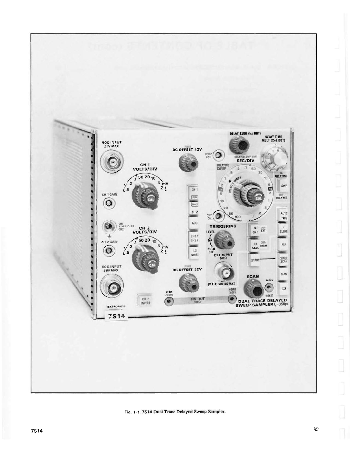
The Tektronix
7S14
Dual Trace Delayed
Sweep
Sampler
is
a general
purpose
sampling unit with a DC-to-1000
MHz
bandwidth.
It
will
operate
in
any Tektronix 7000 Series
mainframe. The front panel terminology is similar to
that
of
conventional oscilloscopes.
The 7S14 has
two
time bases
to
provide "delaying" and
"delayed sweep" operation. The delayed sweep starts after
the
selected delay interval, giving
the
effect
of
a wide-range
sweep operation. The delayed sweep starts after
the
selected delay interval, giving
the
effect of a wide·range
sweep magnifier. The calibrated delay replaces
the
"time
position" control found
on
most sampling time-base units.
The 7S14 has a
two
dot
time-interval measurement
method
that
provides a means
of
measuring
the
time
between
two
points
on
the
"normal"
(delaying) display. A
brightened
dot
on
the
trace can be positioned
to
the
start
of
the
event
to
be measured. A second brightened
dot
can
be
positioned
to
the
end
of
the
event by using
the
Delay
Time Mult control. The time interval between
the
two
points
is
the
product
of
the
reading
on
the
Delay Time Mult
dial times
the
Delaying Sweep Sec/Div setting_
Delay lines
in
the
input signal channels permit display of
the
leading edge of
the
triggering waveform. The Auto
Level
mode provides a bright baseline in
the
absence
of
a
triggering
signal. Other features include 2 mV/div
sensitivity, low tangential noise, versatile triggering capabil-
ities, a broad range of sweep rates, and
crt
readout
of
both
the attenuation and timing
values_
The characteristics given
in
the
following Table apply over
an ambient temperature range from
O°C
to
+50°C after
the
instrument has been calibrated
at
+25°C ±5°C. Under these
conditions,
the
7S14 will perform
to
the
requirements given
in
the
Performance Check section
of
this manual.
The Supplemental Information column
of
the
Table
provides additional information about
the
operation
of
the
7S14. Characteristics given in
the
Supplemental Infor-
mation column are
not
requirements in themselves and are
not
necessarily checked
in
the
Performance Check
procedure.
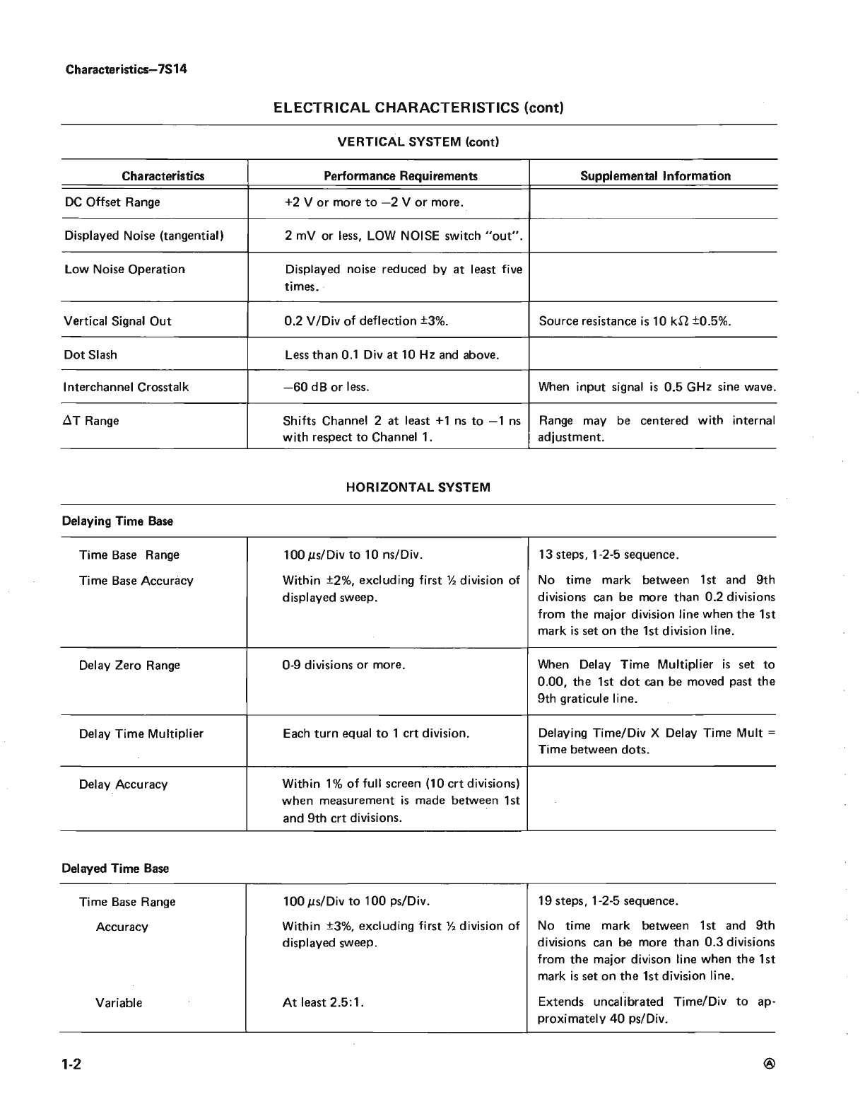
ELECTRICAL CHARACTERISTICS
VERTICAL SYSTEM
Characteristics Performance Requirements Supplemental Information
Risetime 350
ps
or
less, 10%
to
90%
of
step pulse
signal.
Step Aberrations +2%,
-3%,
total
of
5%
or
less
Pop
within Check made with Tektronix 284 Pulse
first 5
ns
after step transition;
+1
%,
-1
%,
Generator; includes aberrations from
the
total
of
2%
or
less
pop
thereafter. 284.
Bandwidth
(-3
dB)
DC
to
1 GHz
or
more. Calculated from risetime.
Input Resistance
50
n within 2%.
Deflection Factor 2 mV/Div
to
0.5 V/Div. 8 steps, 1-2-5 sequence.
Accuracy Within
±3%
(with VARIABLE
at
CAL).
Variable At least 2.5:1. Extends uncalibrated deflection factor
to
approximately
800
I1V
/Div.
Input Signal Range
Maximum Operation 2 V
pop
(DC
+ Peak
AC)
within a +2 V
to
-2
V window
at
any sensitivity.
Maximum Overload
±5V.
REV APR 1982
,-,
Scans by Artekmedia => 2010