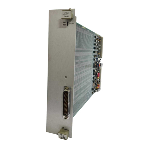
Tektronix P7001 /IEEE 488 User manual

Tektronix®
COMMITTEDTO EXCELLENCE
PLEASE CHECK FOR CHANGE INFORMATION
AT THE REAR OF THIS MANUAL.
P7001 /|EEE 488
INTERFACE
021 -0206-00
INSTRUCTION MANUAL
Tektronix, Inc.
PO. Box 500
Beaverton, Oregon 97077 Serial Number
070-2623-00 First Printing JUL 1978
Product Group 45 Revised DEC 1986

Copyright ©1978 Tektronix, Inc. All rights reserved.
Contents of this publication may not be reproduced in any
form without the written permission of Tektronix, Inc.
Products of Tektronix, Inc. and its subsidiaries are covered
by U.S. and foreign patents and/or pending patents.
TEKTRONIX, TEK, SCOPE-MOBILE, and are
registered trademarks of Tektronix, lnc. TELEQUIPMENT
is aregistered trademark of Tektronix U.K. Limited.
Printed in USA. Specification and price change privileges
are reserved.
INSTRUMENT SERIAL NUMBERS
Each instrument has aserial number on a panel insert, tag,
or stamped on the chassis. The first number or letter
designates the country of manufacture. The last five digits
of the serial number are assigned sequentially and are
unique to each instrument. Those manufactured in the
United States have six unique digits. The country of
manufacture is identified as follows:
8000000 Tektronix, Inc., Beaverton, Oregon, USA
100000 Tektronix Guernsey, Ltd., Channel islands
200000 Tektronix United Kingdom, Ltd., London
300000 Sony/Tektronix, Japan
700000 Tektronix Holland. NV, Heerenveen.
The Netherlands

TABLE OF CONTENTS
SECTION 1GENERAL INFORMATION
SECTION 2INSTALLATION
SECTION 3PROGRAMMING INFORMATION
WARNING
THE FOLLOWING SERVICING INSTRUCTIONS ARE FOR USE BV
QUALIFIED PERSONNEL ONLY. TO AVOID PERSONAL INJURV,
DO NOT PERFORM ANV SERVICING OTHER THAN THAT CONTAINED
IN OPERATING INSTRUCTIONS UNLESS YOU ARE QUALIFIED TO
DO SO.
SECTION 4MAINTENANCE
SECTION 5DIAGRAMS
SECTION 6 REPLACEABLE PARTS
APPENDIX ADATA SHEETS
APPENDIX BHP 9825 PROGRAMMING INFORMATION
APPENDIX CSUPPLEMENTAL INFORMATION
LIST OF ILLUSTRATIONS
Figure Description Page
2—1 Device Address Switch SW412 2-1
Setting The P123 Strap Option 2 2
P7001/IEEE 488 Interface Installation 23
IEEE 488 Bus Connector Pin Assignments 2—4
3 5
38
39
Data Transfer Delimiters &Terminators
P7001 4K Memory Map
DPO Card Address Map
Location of Readout Words and Characters
WWWL‘ONNN
waI—‘DWN
(Timeslots) and Field 0Addresses 3—12
3—5 Status Word Formats 3—14
3—6 HSA Status Register Bit Assignments 3—15
4—1 Basic Block Diagram 4—2
4—2A P7001 Bus Read Operation 4—9
4—2B P7001 Bus Write Operation 4—9
4—3 Funct Block Diag., MPU/GPIB Bd &
Component Locator 4—11
4—4 Funct Block Diag., PIA/P7001 Bd &
Component Locator 4-12
LIST OF TABLES
Table Description Page
1—1 P7001/IEEE 488 Interface Capability 1-2
3—1 Setting Commands 3—6
3—2 Query Commands 3—7

262531‘
P7001/IEEE 488 INTERFACE

P7001/IEEE Interface
Section 1
GENERAL INFORMATION
INTRODUCTION
This manuaI contains both operationaI and maintenance information for the
Tektronix P7001/IEEE 488 Interface, Tektronix Part No. 021—0206-00. This in—
terface is used to interconnect the P7001 Processor section of aTektronix
DigitaI Processing Osci110$cope (DPO) with any of severaI Tektronix manufac-
tured devices designed to operate in accordance with IEEE Standard 488-1975,
”IEEE Standard DigitaI Interface for ProgrammabIe Instrumentation”. The IEEE
488 Bus is commonIy known as the Genera] Purpose Interface Bus (GPIB), and
may be referred to by that name.
Asystem configured from IEEE 488 compatibIe devices is Iimited to amax-
imum of 15 devices, and incIudes asystem controIIer, such as aTektronix
4051 Graphic System, as weII as ”taIkers” and ”Iisteners”. The DPO in such
asystem functions as both ataIker and aIistener. As atalker, the DPO
sends current status messages, data captured by the Acquisition Unit, and
readout information to the system controIIer or other system Iisteners. As
aIistener, it receives commands and data from the system controIIer or other
system devices.
IEEE 488 INTERFACE CAPABILITY
The capabiIities of the P7001/IEEE 488 Interface are defined in TabIe 1-1
by referencing the applicabIe sections of the IEEE Standard 488-1975 document.
PHYSICAL CHARACTERISTICS
The P7001/IEEE 488 Interface is aduaI card assemny designed to be in-
staIIed into the interface sIot of the P7001 Processor section of aUFO. AII
necessary operating power (+5, -5, +15 and —12VDC) is taken from the P7001
Power SuppIy via the P7001 Main Interface Board.

P7001/IEEE Interface
Table 1—1 P7001/IEEE 488 Interface CapabiIity
Interface Function
Source Handshake(SH)
Acceptor Handshake(AH)
TaIker(T)
Listener(L)
Service Request(SR)
Remote—LocaI(RL)
ParaIIeI PoII(pP)
Device CIear(DC)
Device Trigger(DT)
ControIIer(C)
IEEE Std. 488 Section
.10
.11
.12
Interface CapabiIity
CompIete(SH1)
CompIete(AH1)
No “TaIk Only” Mode(T6)
No ”Listen OnIy” Mode(L4)
CompIete (SR1)
None(RLfl)
N0ne(PP¢)
None(DCQ)
None(DTg)
None(cg)
1—2

P7001/IEEE lnterlace
Section 2
INSTALLATION
INTRODUCTION
This section of the manual contains operator/user information for the
Tektronix P7001/IEEE 488 Interface, used to interconnect the P7001 Processor
section of aTektronix Digital Processing Oscilloscope (DPO) with any IEEE
488 compatible device. Included are instructions for selecting the Device
Address and for setting astrap option that facilitates the use of different
controllers.
INSTALLATION
The P7001/IEEE 488 Interface assembly may be installed in aP7001 Proces-
sor using the instructional steps listed on the Installation Diagram, Figure
2—3. Before the interface is installed, however, the IEEE 488 Bus Device Ad-
dress and the P123 Strap Option should be set as explained in the following
paragraphs.
SELECTING DEVICE ADDRESS
Selecting the Device Address is accomplished by setting the 5—bit DIP
switch, SN412 0n the MPU/GPIB board (shown in Figure 2-1), to aunique binary
number. For devices with talk/listen capabilities, such as the DPO, this
number must be between $0000 and 01110 (O to 14 decimal), inclusive.
P/O MPU/GPIB BOARD
670-4882—OX
LSD
‘5
MSD
_1f 23‘* mg U413
,DUDD :
——OPEN— 5,
2623—02
Figure 2—1 Device Address Switch SW412
@2—1

P7001/IEEE Interface
SELECTING DEVICE ADDRESS (Continued)
Each of the five bits is set to 1or Dby five corresponding rocker
switches, numbered 1on the left (Least Significant Digit) to 5on the right
(Most Significant Digit). Note that this is reversed from the order in
which the numbers are read. When arocker switch is pushed in at the top,
that bit has been set to abinary 1; e.g., if the first two switches on the
left are pushed in at the top and the other three are in at the bottom, the
Device Address is set to Qflflll (3 decimal).
When the DPO memory location button 'D' is pushed in, the Device Address
that has been selected with SN412 will be displayed in the lower right-hand
corner of the CRT. Note that when Device Address is elicited, any data pre-
viously stored at Channel 7of memory 'D' (Field 0) will be destroyed.
SETTING P123 STRAP OPTION
The P123 strap option allows the interface to operate more efficiently
with different controllers. Amore thorough explanation of use of the strap
option may be found in Section 3of this manual. Figure 2-2 shows connector
P123 set for both "Standard" operation (jumper not installed) and ”Optional"
operation (pin 1jumpered to adjacent pin -pin 1is indicated withu»).
P123633 :2 g81 P123 fig: m873
I; aaaaEflifl 8E
U122 U123 U122 U123
(a) Standard Operation (b) Optional OperatiozréS23 03
l
Figure 2—2 Setting the P123 Strap Option
Access to the jumper is gained through ahole in the left rear of the in—
terface housing (see Figure 2—3). To change operating modes, remove the plug
from the hole and reach in with longnose pliers to re—position the jumper.
To avoid loss when operating in the "Standard“ mode, the jumper may be placed
on pin 1or the adjacent pin (above pin 1) with the free end extending to the
left. If the DPO was energized while the jumper was re-positioned, it must
now be de—energized and a”power—up” sequence performed to activate the change.
2—2 @
P7001/IEEE Inlertace
INSTALLATION/REMOVAL
1.
2. Tighten both interface installation screws.
.Connect either end of the IEEE 488 bus cable (Tektronix Part No.
.Prior to removal, set the AC power to OFF and ensure that the in-
021—0206-00
P700l/IEEE 488 Interface
Interface
Installation
Screws (2)
Cable Assy
012—0630—01
SW412
(Behind Side Panel)
With AC power off, insert the interface into the rear of the P7001
Processor and press in slowly until the assembly is firmly seated.
012-0630—01) to the interface assembly at J1 and secure with thumb—
screws.
terface installation screws and thumbscrews are fully disengaged.
.2623-04
Figure 2—3 P7001/IEEE 488 Interface Installation
2-3

P7001/IEEE Interface
IEEE 488 BUS CONNECTOR
The IEEE 488 Bus Connector is located at the rear panel of the interface,
as shown on Figure 2-3, and is physically attached to the MPU/GPIB Board.
This 24-pin female ribbon connector has attached 16 active signal lines and
8interlaced ground lines, and is used to interconnect the DPO with asystem
controller or other IEEE 488 compatible device. Figure 2—4 shows the con-
nector pin arrangement and signal line nomenclature.
The interface also includes the mating connector and cable, Tektronix
Part No. 012-0630—01 (standard 2meter IEEE 488 cable). This connector is
double—sided, with amale side to mate with the connector on the interface
and afemale side for connecting additional system components to the bus.
SHIELD SRO NDAC DAV Dl04 DIOZ
ATN IFC NRFD EOI D|03 DI01
GND GND GND REN D|O7 DIOS
11 97
LOGIC GND GND GND DIOB DIOG
GND ‘0 86
Figure 2-4 IEEE 488 Bus Connector Pin Assignments
2—4 @

P7001/IEEE Interface
Section 3
PROGRAMMING INFORMATION
INTRODUCTION
This section of the manual contains operator/user information both of a
general nature and for aspecific type of system utilizing the Tektronix
4051 Graphic System as system controller. Included are commands and command
formats used to operate the DPO under program control from any IEEE 488 com-
patible controller. Examples given are in the TEK 4051 BASIC language.
For non-Tektronix controllers, such as the HP—9825 and HP—9830, famil—
iarity with the programming language of the system controller is essential.
Regardless of which controller is being utilized, familiarity with the oper—
ation of the DPO, or use of the DPO Operators Manual will be useful, as will
an understanding of IEEE Standard 488—1975, ”IEEE Standard Digital Interface
for Programmable Instrumentation”.
In addition, for non—Tektronix controllers, the paragraph entitled "Strap
Option“ in this section of the manual, and the corresponding instructions in
Section 2for setting the strap option, must be read and understood. Addi-
tional information on use with the HP—9825 is contained in Appendix II at the
rear of this manual.
GENERAL INFORMATION
The P7001/IEEE 488 Interface can be used to interconnect any IEEE 488
compatible device with the P7001 bus of aTektronix Digital Processing Os-
cilloscope (0P0). There are three different types of devices on the IEEE
488 bus; ”controllers”, "talkers”, and "listeners”. IEEE Standard 488—1975
allows specific listeners and talkers to be selected and de-selected inde—
pendently. The responsibility of the controller is to designate which sys-
tem connected instruments are to listen or to talk. The DPO in such asys-
tem functions as both atalker and alistener. As atalker, it sends data
captured by the DPO (i.e., waveforms), current status messages, and grati—
cule readout information to the bus. As alistener, the DPO receives data
(waveforms), commands, and internal memory addresses from the bus.
OPERATING INSTRUCTIONS
Most of the operating instructions included here are specifically for
use with aTEK 4051 Graphic System as system controller. Operating instruc-
tions for other IEEE 488 controllers may be inferred from acomparison of
the instructions included here and those for the controller utilized. An
appendix to this manual gives operating examples for the HP-9825 controller.
Power On/Initialization
When aDPO goes through the power—on transition, it automatically gener—
ates (through the interface) an interrupt request (SRQ) signal on the IEEE
488 bus. This condition may be cleared and the nature and source of the in—
terrupt determined by programming the controller to take aserial status
poll, as shown in asubsequent paragraph entitled ”Servicing Interrupts with
the TEK 4051".
@3—1

P7001/IEEE Interface
Power On/Initialization (Continued)
If no interrupt handling instructions are included in the program, or
for some other reason the controller does not service the interrupt, the
interface must be cleared. This can be accomplished by using the ”DCLb“
command explained later in this section.
Status Word
The DPO Status Word is used to indicate to the controller the reason
for aDPO interrupt request (SR0), or may be solicited with aPOLL state-
ment, When no SRQ has been generated, the interface will respond with one
of the following decimal status words:
Status Word 0Meaning: Interface idle (Both cases return decimal
l6 2Interface busy 16 with HP controllers)
When the DPO issues an interrupt, its interface asserts the SRQ signal
line on the IEEE 488 bus. The system controller should be programmed to
conduct astatus poll in order to release the SRQ. The interface will res-
pond with one of the following decimal status words (the DPO will issue an
interrupt request for each of these conditions):
Status Word =81 Meaning DPO powered up.
=82 DPO was hung but has self— corrected.
=83 :DPO PROGRAM CALL button pushed.
=84 :DPO Single Sweep completed.
=85 :HSA aborted (if HSA is installed).
>18¢ :Error has occurred (see following para-
graph entitled "Error Messages").
Error Messages
Four different error conditions may exist for the DPO; each will be in-
dicated to the system controller by an SRQ. Astatus poll conducted after
receipt of the SRQ will result in one of the following decimal status words:
Status Word 113 Meaning: Communication Error -the data input is
meaningless or impossible to implement.
If the data will affect the DPO operation,
the error is not acommunication error.
Examples include parity errors, unintel-
ligible commands, or syntax errors.
114 :Programming Error —intelligible commands
have been received which involve out of
range parameters. The DPO attempts to
carry out the assigned operation but finds
it impossible to complete. Examples in-
clude overflowing DPO data size, and in-
valid addressing of the DPO internal mem—
ory.
115 :Internal Error —an Interface or P7001
hardware error has occurred. This may
mean apermanent hardware malfunction or
atransient condition.
112 :Other Error -the DPO has discovered an
error which is none of the previously de-
scribed cases.
3—2 @

P7001/IEEE Interface
Servicing Interrupts with the TEK 4051
When the UPC issues an interrupt service request (SRQ) through the
interface, the 4051 is normally programmed to finish executing the current
statement, then transfer to an interrupt handling routine, as shown in the
following example:
lflfl 0N SRQ THEN SUM
50¢ POLL N,M;4;5;1
51¢ PRINT N,M
52$ GOTO N0F 6$¢,7¢¢,8QQ
BOO IF M=83 THEN 4flww
81% IF M=84 THEN 599$
82¢ RETURN
4QQQ (service routine for DPO Front Panel PROGRAM CALL buttons)
429w RETURN
SOOO (service routine for DPO Single Sweep)
519$ RETURN
In the foregoing example, line 1PM enables the 4051 to respond to an SRO
condition; the program then executes in normal sequential order. When the
DPO (or any other peripheral device) signals an SRQ, the 4051 finishes the
present statement, then transfers to the POLL statement at line SEE. The
POLL statement contains the two numeric variables Nand Mas parameters fol-
lowed by device addresses 4,5,1. As the 4051 executes the POLL statement,
it first addresses device number 4to see if it is requesting service. As—
suming the DPO has been assigned device address 1, the 4051 will continue to
poll devices in the order shown until it reaches device 1. When the 4051
finds that device 1issued the SRQ, it assigns the number §_to variable N
in the POLL statement, because device 1is the third device on the list.
The DPO returns adecimal status word (previously explained) which is
assigned to the variable M. Line 51% causes Nand Mto be printed on the
4051 screen. Line 52¢ sends the program to N, or the third (8QQ) line num-
ber in the list 6¢¢,7Q¢,8¢¢. In line 89¢, if the status word (M) is 83 the
program moves to line 4OQQ, which begins aservice routine for the DPO PRO-
GRAM CALL buttons. Line 81¢ performs the same function for status word 84.
If the 4051 does not have the DPO's device address in its program (list—
ed in the POLL statement) when an SRQ is received, processing will halt and
the 4051 will ”hang” pending further instructions. At this point, the oper-
ator should find the line containing the POLL statement and re-enter the
statement so that the list of devices to be polled includes the DPO. Subse—
quent status polls will then recognize the address.
NOTE
This condition will not occur when using
the HP—9825 as system controller, because
it will time out and resume processing if
unable to identify adevice.
@3-3

P7001/IEEE Interface
Servicing Interrupts with the TEK 4051 (Continued)
If the TEK 4051 is being used as system controller but is idle, or does
not have interrupt handling instructions in its program, the following error
message will be printed on the screen when an SRQ is received:
NO SRQ 0N UNIT -MESSAGE NUMBER 43
To clear this condition, the operator should enter the following statement
in the immediate mode (no line number):
POLL N,M;(DPO Device Address)
Strap Option
The IEEE 488-1975 standard is ahardware standard. As such, its main
purpose is to confirm the electrical characteristics of the interface bus
and the handshake procedures, addressable messages, unaddressable messages,
and universal messages. It does not specify the delimiters and terminators
that pass through the bus together with the data and command information.
Astrap option is provided to allow the user to set the interface to send
or accept different kinds of delimiters and terminators.
Implementation of the strap option is described and illustrated in Sec—
tion 2of this manual. The option provides two operating modes, ”Standard”
operation and ”Optional” operation. Standard operation is defined as be—
tween the DPO and aTektronix controller, such as the TEK 4051. Optional
operation should be used with Hewlett-Packard controllers, such as the HP-
9825, to speed up transfer time, use less core, and ease programming.
Delimiters and terminators used for Standard data transfers are as fol-
lows:
Accepts into DPO: delimiters ",” or "b” or ”CR” or ”LF" or any combination.
:terminators -any character with EOI asserted.
Sends to controller: delimiter ”,”
:terminator —the sequence of "CR”, then ”LF” with
EOI asserted.
Delimiters and terminators used for Optional data transfers are as fol—
lows:
Accepts into DPO: delimiters -same as for Standard operation.
:terminators -“LF” without EOI asserted, pp_any char—
acter with EOI asserted.
Sends to controller: delimiter and terminator —same as standard operation.
The characters used above and their ASCII decimal equivalents are as
follows (the complete ASCII code chart is included as asupplement to this
manual). ",” =comma (ASCII 44)
"CR” = CARRIAGE RETURN (ASCII 13)
l'LF" =LINE FEED (ASCII 10)
"b” =space (ASCII 32)
E01 =End Or Identify (IEEE 488 bus management signal).
3-4

.,P7001HEEE hflenace
Strap Option (Continued)
Use of the delimiters and terminators is illustrated in Figure 3-1, which
shows the last four elements of adata (waveform) transfer from the DPO to
the controller. The strap option is set for “Standard”.
Termination
Characters Waveform
\Elemi 512 Elemi 511 Elem.I 510 Elemeht 509
lIllI I IIl
Data to
-Cbntroller
EOI Lin ..7
eDelimiter Characters
262335
Figure 3—1 Data Transfer Delimiters and Terminators
COMMAND FORMAT
The general command format (the sequence in which commands occur) is as
follows: (MTA or MLA)(DAB).
Where: MTA (My Talk Address) and MLA (My Listen Address) are the primary
addresses used to command the DPO to transmit data (talk) or re—
ceive data (listen), respectively: MTA and MLA are identical to
the I/O Address referred to in the TEK 4051 manual, and may col-
lectively be referred to as Hardware Unit Number (HUN) or Device
Address. Instructions for setting this address are in Section 2
of this manual.
DAB (Command Data Bytes) consist of three data bytes of ASCII
characters followed by either aquestion mark or ablank space
(both also ASCII).
NOTE
The Secondary Address (MSA) described in
the IEEE 488—1975 standard is not appli-
cable to this interface.
Depending on the intended operation, commands from the system controller
may be received in one of three specific formats, as follows:
Write to DPO —This command format consists of the DPO's Device Address
(MLA in this case), then athree character mnemonic from
the Setting Commands of Table 3-1 followed by aspace,
then the data to be sent to the DPO [i.e., (MLA)(DABb)data].
@3-5

P7001/IEEE lnterlace
COMMAND FORMAT (Continued)
Set DPO to be -This command format consists of the DPO Listen Address,
read
Read from DPO -
then athree character mnemonic from the Query Commands
of Table 3-2 followed by aquestion mark [i.e., (MLA)(DAB?)].
This command asks the DPO aquestion that it (the DPO)
will not be able to answer until the "Read from DPO" op—
eration is executed.
This command format consists only of the assignment of
the DPO as talker, after which the requested information
is sent from the DPO. The terminating characters (”CR",
then ”LF” with EOI asserted) are generated automatically
by the interface. Before a”Read from DPO” operation
can be performed, the "Set DPO to be read“ operation
must be executed.
Table 3-1 Setting Commands
ADR
CHL
CLI
DAT
DCL
DPA
DPB
DPC
DPD
HAV
HIS
HOL
OCT
SCL
SSR
STO
TAB
TAC
TAD
TBA
TBC
TBD
TCA
TCB
Address
Channel
Clear (F
Data
Device C
Waveform
Waveform Bof DPO Memory is selected
Waveform
Waveform Dof DPO Memory is selected
Hardware
Histogra
Hold
Octal
Scale Fa
Single Sweep Reset
Store
Transfer
Transfer
Transfer
Transfer
Transfer
Transfer
Transfer
Transfer
Transfer
Transfer
Transfer
Transfer
Word
Set DPO
Set DPO
Page: 3-9
3-11
ront Panel) Interrupt 3-19
-O
lear -0
Aof DPO Memory is selected —
Cof DPO Memory is Selected
Average (if HSA is installed)
m(if HSA is installed)
ctor
Waveform Ato Waveform B
Waveform Ato Waveform C-
Waveform Ato Waveform D—
Waveform Bto Waveform A-
Waveform Bto Waveform C-
Waveform Bto Waveform D-
Waveform Cto Waveform A-
Waveform Cto Waveform B—
Waveform Cto Waveform D—
Waveform Dto Waveform A-
Waveform Dto Waveform B—
Waveform Dto Waveform C-
to X—Y Display Mode
to Y-T Display Mode
combowwwwwwwwwwwoowwcowwwwwwwwww
I—II—ll—JNNNNNNNNNNNNl—‘l—JI—lI—JI—‘I—lI—JOOOOmmNH
WOOOOOOOOOOOOOOONNLQO‘DNCOOO
3—6 @

P7001/IEEE Interface
COMMAND DESCRIPTIONS
Commands from the IEEE 488 controller are structured in one of two ways.
Setting Commands are used to transfer data to or set the status of the DPD,
and are structured as athreeacharacter mnemonic followed by ablank space,
enclosed by quotation marks, such as ”ADRW" (the character bis used to des-
ignate ablank space). The Setting Commands are shown in Table 3—1.
The Query Commands, used to transfer data or status information from the
DPD to the controller, consist of athree-character mnemonic followed by a
question mark, enclosed by quotation marks. Using the Address command again
as an example, this would look like ”ADR?”. The Query Commands are shown
in Table 3—2.
Table 3—2 Query Commands
ADR? Address Page:
DAT? Data
DPA? Send Waveform Aof DPO memory
DPB? Send Waveform Bof DPO memory
DPC? Send Waveform Cof DPO memory
DPD? Send Waveform Dof DPO memory
wwwwwwwwww
IHl—‘l—‘l—‘KOKDKOLDI—IKO
FPI? Front Panel Interrupt -9
OCT? Octal -6
SCL? Scale Factor -1
WRD? Word —1
DATA TRANSFER
The DPO memory contains four waveform locations, designated A, B, Cand
D, Each waveform is a512-element array. The data for each element is an
integer in the range Dto 1D23 (decimal). Figure 3-2 shows amemory map for
aP7001 4K memory. At the top are four blocks labeled A, B, Cand D. These
blocks represent the four waveform locations in memory as selected from the
DPD front panel. Each waveform location has an address range of 512 (deci-
mal). Waveform A, for example, is DDD to 511, Waveform Bis 512 to 1D23,
etc.
Data may be transferred to and from the DPD in three different ways, as
follows:
1. Use of the DPA, DPB, DPC and DPD commands;
2. Use of the ADR and DAT commands;
3. Use of the ADR and WRD commands.

P7001/IEEE Interface
[WAVEFORM A41
LwAVEFORM B
[WAVEFORM cI
IWAVEFORM D7
Field 0
(Scale Factors) A
.
BCD
2¢48 212 176 225
Field 1D
(Messages) lAB
.
C
2568 2639 2688 2767 2816 2895 2944
Field 2
(Messages) lA B C D
3972 3279 3328 3497 3456 3535 3583
Field 3i
(Messages) A
.,
BJCD
3584 3663 3712 3791 3849 3919 3968 4fl47 4095
2623-06
Figure 3—2 P7001 4K Memory Map
DPA, DPB, DPC and DPD Commands
The DPA, DPB, DPC and DPD commands are used to transfer 512 data words,
or waveform elements, to or from DPO memory locations A, B, Cand D, respect-
ively. Data transfers from the DPD to the controller are normally performed
after ”Store" and llHold” operations in the DPD. Store and Hold operations
may be performed using the ”STOb" and ”HOLb” commands explained later, or
may be executed manually from the DPO Front Panel (see DPO Operators Manual,
Tektronix P/N 070-1599-00).
Asingle blank space after the command mnemonic, such as ”DPAb" or "DPCb"
indicates adata transfer from the TEK 4051 to the DPD. The command is de—
limited with asemicolon. The following TEK 4051 example shows how a512-
element array, Z, would be transferred from the controller to Waveform loca—
tion Aof aDPO with aDevice Address of 1:
PRINT @1:”DPA ”,Z;
Note the use of the delimiter (g) after the Zcharacter. This speeds up da—
ta transfer time in the 4051. If it is not used, the 4051 will send up to
six spaces between each data word, depending on the number of digits of the
data.
3-8 @

P7001/IEEE Interface
DPA, DPB, DPC AND DPD Commands (Continued)
When the command mnemonics DPA, DPB, DPC and DPD are followed by aques—
tion mark, such as "DPA?" or ”DPC?”, the interface is set up to allow data
to be transferred from the DPO to the controller or other IEEE 488 bus list—
ener. In the following TEK 4051 example, line 90 dimensions Bto a512 ele-
ment array, line 100 outputs the ASCII characters ”DPB?” to the bus and sets
up the DPO to output the requested data, and line 110 inputs the 512 data
words of the Device Address 1(the DPD), Waveform B, into the 4051.
90 DIM 8(512)
100 PRINT @1:”DPB?”
110 INPUT @lzB
ADR Commands
The “ADRb” (Address) command is used to set up the DPO Address Register
residing in the interface. It allows the controller to select each memory
cell independently. The addressable DPO memory is from decimal 0to 8191.
(See Figure 3-2, ”P7001 4K Memory Map”, and Figure 3—3, ”DPO Card Address
Map"). The following TEK 4051 example shows Device Address 1, the DPO, ad—
dress 2560 (the start of Field 1) being selected:
PRINT @1:“ADR ”;2560
Note that the argument following the command mnemonic (2560 in the above ex-
ample) may also be anumeric variable that is defined elsewhere in the prog—
ram.
The ”ADR?“ command is used to set the DPD ready to output the current
status of its address register when assigned to talk. In the following TEK
4051 example, line 100 readies the DPO to talk, and line 110 assigns the DPO
to talk and the controller to listen.
100 PRINT @1:ADR?"
110 INPUT @lzP
HSA lst WAVEFORM *
4096
608
HSA 2nd WAVEFORM *
120
5632
6144
HSA CONT‘IHM}* FRONT PANEL,
6656 6912 7040
DISPLAY GEN READOUT INTFC A/D CONVERTER I/O INTERFACE
7168 7296 424 552
DISPLAY GENERATOR, X—Y MODE, XDATA
7680
*If HSA is installed 2623~07
Figure 3-3 DPO Card Address Map
@3-9

P7001/IEEE Interface
DAT Commands
The DAT (Data) commands allow 512 elements of data to be transferred to
or from the DPO, with the beginning address pointed to by the DPO Address
Register (set up with the ”ADRb” command). After execution of these commands,
the DPO Address Register is advanced by decimal 512.
In the following TEK 4051 example, line SOD dimensions the array Yto
512 elements, line 51% defines Y, line 6DD sets the Address Register of the
DPO to 256, and line 61¢ actually transfers array Yfrom the 4051 to the DPO
(into the second half of Waveform location Aand the first half of Waveform
location B). After line 61D, the DPO Address Register will be at 768.
SOD DIM Y(512)
51¢ LET Y=10¢
6D¢ PRINT @1:"ADR ”;256
61¢ PRINT @1:”DAT ",Y;
Note the delimiter (g) after Yin line 61%. This is explained after the
“DPAb” command example in aprevious paragraph.
In the following TEK 4051 example, line 1WD dimensions array Xto 512
elements, line 119 sets the Address Register of the DPO to 256, or the ad-
dress of the beginning of the second half of Waveform A(see Figure 3—2),
line 12% readies the DPO to talk, and line 13D transfers the 512 data words
from the DPO to the controller. After completion of this sequence, array X
is holding the second half of Waveform Aand the first half of Waveform B.
IOD DIM X(512)
11% PRINT @1:"ADR ",256
12D PRINT @1:”DAT?”
13¢ INPUT @1:X
WRD Commands
The WRD (word) commands allow the 10 bits of aDPO data word to be trans—
ferred to or from the DPO (in decimal form). The ”ADRb“ command is used to
set up the DPO Address Register. After execution of either of the WRD com-
mands, the Address Register is automatically incremented by 1. These com—
mands can be used to transfer an array of nelements to or from the DPO,
where nis defined by the controller.
In the following TEK 4051 example, the array Yis first dimensioned to
1D24 elements in line 5WD, Yis defined in line 510, then line 52% sets the
Address Register of the DPO to 512, or the beginning of Waveform B. Lines
53% and 55D perform the FOR LOOP function of the 4051, and line 54% transfers
the 1D24-element array, one word at atime, to DPO memory (Waveforms Band C).
SOD DIM Y(1Q24)
51¢ LET Y=50D
52% PRINT @1:”ADR ”,512
53¢ FOR N=1 to 1024
549 PRINT @1:"WRD ";Y(N)
55¢ NEXT N
3—10 @
Table of contents
Other Tektronix Recording Equipment manuals

Tektronix
Tektronix TekConnect Probe Interface Module 80A03 User manual

Tektronix
Tektronix 73A-451 User manual

Tektronix
Tektronix MTX100A User manual

Tektronix
Tektronix DD 501 User manual

Tektronix
Tektronix DD 501 User manual

Tektronix
Tektronix 7S14 User manual

Tektronix
Tektronix FG 502 User manual

Tektronix
Tektronix 7S14 User manual

Tektronix
Tektronix MTX100 User manual
Popular Recording Equipment manuals by other brands

Lochinvar
Lochinvar SMART TOUCH w/CON-X-US Service manual

Peak
Peak PCAN-ISA user manual

Bunker Hill Security
Bunker Hill Security Power drive BPD-1 user guide

Dell
Dell DIGIRAD N Operating instructions and warnings

Behringer
Behringer FEEDBACK DESTROYER PRO DSP1124P manual

JK Audio
JK Audio InlinePatch user guide