Tews Technologies TCP460 User manual

The Embedded I/O Company
TCP460
16 Channel Serial Interface RS232/RS422
Version 1.0
User Manual
Issue 1.1
October 2005
D74460800
TEWS TECHNOLOGIES GmbH
Am Bahnhof 7 25469 Halstenbek / Germany
Phone: +49-(0)4101-4058-0 Fax: +49-(0)4101-4058-19
TEWS TECHNOLOGIES LLC
1 E. Liberty Street, Sixth Floor Reno, Nevada 89504 / USA
Phone: +1 (775) 686 6077 Fax: +1 (775) 686 6024

TCP460 User Manual Issue 1.1 Page 2 of 32
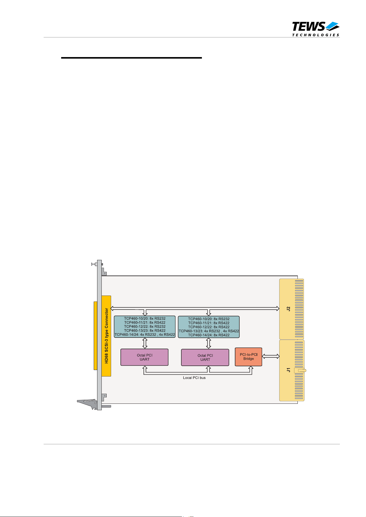
TCP460-10
16 channel RS232 asynchronous serial interface,
front panel I/O
TCP460-11
16 channel RS422 asynchronous serial interface,
front panel I/O
TCP460-12
8 channel RS232, 8 channel RS422
asynchronous serial interface, front panel I/O
TCP460-13
12 channel RS232, 4 channel RS422
asynchronous serial interface, front panel I/O
TCP460-14
4 channel RS232, 12 channel RS422
asynchronous serial interface, front panel I/O
TCP460-20
16 channel RS232 asynchronous serial interface,
front panel and J2 I/O
TCP460-21
16 channel RS422 asynchronous serial interface,
front panel and J2 I/O
TCP460-22
8 channel RS232, 8 channel RS422
asynchronous serial interface, front panel and
J2 I/O
TCP460-23
12 channel RS232, 4 channel RS422
asynchronous serial interface, front panel and
J2 I/O
TCP460-24
4 channel RS232, 12 channel RS422
asynchronous serial interface, front panel and
J2 I/O
This document contains information, which is
proprietary to TEWS TECHNOLOGIES GmbH. Any
reproduction without written permission is forbidden.
TEWS TECHNOLOGIES GmbH has made any
effort to ensure that this manual is accurate and
complete. However TEWS TECHNOLOGIES GmbH
reserves the right to change the product described
in this document at any time without notice.
TEWS TECHNOLOGIES GmbH is not liable for any
damage arising out of the application or use of the
device described herein.
Style Conventions
Hexadecimal characters are specified with prefix 0x,
i.e. 0x029E (that means hexadecimal value 029E).
For signals on hardware products, an ‚Active Low’ is
represented by the signal name with # following, i.e.
IP_RESET#.
Access terms are described as:
W Write Only
R Read Only
R/W Read/Write
R/C Read/Clear
R/S Read/Set
2005 by TEWS TECHNOLOGIES GmbH
Issue Description Date
1.0 First Issue June 2005
1.1 Configuration EEPROM data & Pinout clarification October 2005

TCP460 User Manual Issue 1.1 Page 3 of 32
Table of Contents
1PRODUCT DESCRIPTION......................................................................................... 5
2TECHNICAL SPECIFICATION................................................................................... 6
3CPCI/PCI INTERFACE ............................................................................................... 8
3.1 Secondary PCI Bus Overview........................................................................................................9
3.2 PCI2050B PCI-to-PCI Bridge General Info ....................................................................................9
4XR17D158 OCTAL PCI-UART ................................................................................. 10
4.1 PCI Configuration Space Registers (PCR) .................................................................................10
4.2 Device Configuration Space ........................................................................................................11
4.2.1 UART Register Sets...........................................................................................................12
4.2.2 Device Configuration Registers .........................................................................................13
4.2.3 UART Configuration Registers...........................................................................................14
4.3 Configuration EEPROM................................................................................................................16
5CONFIGURATION HINTS ........................................................................................ 19
6PROGRAMMING HINTS .......................................................................................... 20
6.1 UART Baud Rate Programming...................................................................................................20
7PIN ASSIGNMENT – I/O CONNECTOR .................................................................. 22
7.1 Front Panel I/O Connector ...........................................................................................................23
7.1.1 TCP460-x0 .........................................................................................................................23
7.1.2 TCP460-x1 .........................................................................................................................24
7.1.3 TCP460-x2 .........................................................................................................................25
7.1.4 TCP460-x3 .........................................................................................................................26
7.1.5 TCP460-x4 .........................................................................................................................27
7.2 CompactPCI Back I/O ...................................................................................................................28
7.2.1 TCP460-20.........................................................................................................................28
7.2.2 TCP460-21.........................................................................................................................29
7.2.3 TCP460-22.........................................................................................................................30
7.2.4 TCP460-23.........................................................................................................................31
7.2.5 TCP460-24.........................................................................................................................32

TCP460 User Manual Issue 1.1 Page 4 of 32
Table of Figures
FIGURE 1-1 : BLOCK DIAGRAM......................................................................................................................5
FIGURE 2-1 : TECHNICAL SPECIFICATION...................................................................................................7
FIGURE 3-1 : CPCI/PCI INTERFACE...............................................................................................................8
FIGURE 3-2 : SERIAL CHANNEL MAPPING ...................................................................................................8
FIGURE 3-3 : SECONDARY PCI BUS OVERVIEW.........................................................................................9
FIGURE 4-1 : XR17D158 PCI HEADER .........................................................................................................10
FIGURE 4-2 : DEVICE CONFIGURATION SPACE........................................................................................11
FIGURE 4-3 : UART REGISTER SET OFFSET .............................................................................................12
FIGURE 4-4 : UART REGISTER SET ............................................................................................................12
FIGURE 4-5 : DEVICE CONFIGURATION REGISTERS ...............................................................................13
FIGURE 4-6 : UART CHANNEL CONFIGURATION REGISTERS ................................................................14
FIGURE 4-7 : CONFIGURATION EEPROM TCP460-XX ..............................................................................16
FIGURE 4-8 : PHYSICAL CONFIGURATION EEPROM DATA OF UART 1 .................................................17
FIGURE 4-9 : PHYSICAL CONFIGURATION EEPROM DATA OF UART 2 .................................................18
FIGURE 5-1 : UART INTERFACE MAPPING.................................................................................................19
FIGURE 6-1 : UART BAUD RATE PROGRAMMING .....................................................................................20
FIGURE 7-1 : TCP460-X0 PIN ASSIGNMENT FRONT PANEL I/O CONNECTOR ......................................23
FIGURE 7-2 : TCP460-X1 PIN ASSIGNMENT FRONT PANEL I/O CONNECTOR ......................................24
FIGURE 7-3 : TCP460-X2 PIN ASSIGNMENT FRONT PANEL I/O CONNECTOR ......................................25
FIGURE 7-4 : TCP460-X3 PIN ASSIGNMENT FRONT PANEL I/O CONNECTOR ......................................26
FIGURE 7-5 : TCP460-X4 PIN ASSIGNMENT FRONT PANEL I/O CONNECTOR ......................................27
FIGURE 7-6 : PIN ASSIGNMENT TCP460-20 COMPACTPCI BACK I/O CONNECTOR (J2)......................28
FIGURE 7-7 : PIN ASSIGNMENT TCP460-21 COMPACTPCI BACK I/O CONNECTOR (J2)......................29
FIGURE 7-8 : PIN ASSIGNMENT TCP460-22 COMPACTPCI BACK I/O CONNECTOR (J2)......................30
FIGURE 7-9 : PIN ASSIGNMENT TCP460-23 COMPACTPCI BACK I/O CONNECTOR (J2)......................31
FIGURE 7-10 : PIN ASSIGNMENT TCP460-24 COMPACTPCI BACK I/O CONNECTOR (J2)....................32

TCP460 User Manual Issue 1.1 Page 5 of 32
1 Product Description
The TCP460 is a standard 3U 32 bit CompactPCI module and offers 16 channels of high performance
serial interface.
Five different standard modules are available: The TCP460-10 provides 16 RS232 interfaces. The
TCP460-11 provides 16 RS422 interfaces. The TCP460-12 provides 8 RS232 and 8 RS422
interfaces. The TCP460-13 provides 12 RS232 and 4 RS422 interfaces. The TCP460-14 provides 4
RS232 and 12 RS422 interfaces. Other configurations are available as factory option on a per channel
basis.
All modules offer front panel I/O with a HD68 connector. The TCP460-2x modules offer additional J2
rear I/O. Each RS232 channel supports RxD, TxD, RTS and CTS. Each RS422 supports RxD+/- and
TxD+/-.
A transparent 32 bit / 66 MHz PCI-to-PCI Bridge provides access to the two Exar XR17D158 octal
PCI-UARTs. The PCI-to-PCI Bridge allows 32 bit accesses on the local PCI bus and permits the high
data throughput necessary for the high performance serial interfaces.
Each channel has 64 byte transmit and receive FIFOs to significantly reduce the overhead required to
provide data to and get data from the transmitters and receivers. The FIFO trigger levels are
programmable and the baud rate is individually programmable up to 921.6 kbps for RS232 channels
and 5.5296 Mbps for RS422 channels. The UART offers readable FIFO levels.
Interrupts are supported. For fast interrupt source detection each octal UART provides a special
Global Interrupt Source Register.
All serial channels use ESD protected transceivers up to ±15KV according to IEC 1000-4-2.
The TCP460 can operate with 3.3V and 5.0V PCI I/O signaling voltage.
Figure 1-1 : Block Diagram

TCP460 User Manual Issue 1.1 Page 6 of 32
2 Technical Specification
PMC Interface
Mechanical Interface Standard 3U 32 Bit CompactPCI module conforming to
PICMG 2.0 R3.0
Electrical Interface PCI Rev. 2.3 compliant
33 MHz / 32 bit PCI
3.3V and 5V PCI Signaling Voltage
On Board Devices
PCI-to-PCI Bridge PCI2050B (Texas Instruments)
Octal UART XR17D158 (Exar)
Transceiver RS232: MAX3225E (or equivalent)
RS422: MAX3087E (or equivalent)
I/O Interface
Interface Type Asynchronous serial interface
Number of Channels 16 (2x 8 channels)
Physical Interface TCP460-x0: 16 RS232
TCP460-x1: 16 RS422
TCP460-x2: 8 RS232, 8 RS422
TCP460-x3: 12 RS232, 4 RS422
TCP460-x4: 4 RS232, 12 RS422
Serial Channel I/O Signals RS232: TxD, RxD, RTS, CTS, GND
RS422: TxD+/-, RxD+/-, GND
Termination RS422: 120Ωbetween RxD+ and RxD- of each channel
Programmable Baud Rates RS232: up to 921.6 kbps
RS422: up to 5.5296 Mbps
ESD Protection RS232:
±15kV—Human Body Model
±8kV—IEC 1000-4-2, Contact Discharge
±15kV—IEC 1000-4-2, Air-Gap Discharge
RS422:
±15kV—Human Body Model
I/O Connector HD68 SCSI-3 type connector (e.g. AMP# 787082)
TCP460-2x: additional 110 pol. CompactPCI back I/O (J2)
Physical Data
Power Requirements TCP460-x0: 80 mA typical @ +3.3V DC (no load)
TCP460-x0: 70 mA typical @ +5V DC
TCP460-x1: 120 mA typical @ +3.3V DC (no load)
TCP460-x1: 70 mA typical @ +5V DC
TCP460-x2: 100 mA typical @ +3.3V DC (no load)
TCP460-x2: 70 mA typical @ +5V DC
TCP460-x3: 90 mA typical @ +3.3V DC (no load)
TCP460-x3: 70 mA typical @ +5V DC
TCP460-x4: 110 mA typical @ +3.3V DC (no load)
TCP460-x4: 70 mA typical @ +5V DC

TCP460 User Manual Issue 1.1 Page 7 of 32
Temperature Range Operating
Storage
-40°C to +85°C
-55°C to +125°C
MTBF TCP460-10: 510 000h
TCP460-11: 390 000h
TCP460-12: 440 000h
TCP460-13: 440 000h
TCP460-14: 390 000h
TCP460-20: 470 000h
TCP460-21: 370 000h
TCP460-22: 410 000h
TCP460-23: 440 000h
TCP460-24: 390 000h
Humidity 5 – 95 % non-condensing
Weight 135 g
Figure 2-1 : Technical Specification

TCP460 User Manual Issue 1.1 Page 8 of 32
3 cPCI/PCI Interface
The TCP460 uses two Exar XR17D158 octal PCI-UARTs to provide and control the 16 serial
channels. A transparent 32 bit / 66 MHz PCI-to-PCI Bridge provides access to the two octal PCI-
UARTs. The PCI-to-PCI Bridge allows 32 bit accesses on the local PCI bus and permits the high data
throughput necessary for the high performance serial interfaces.
Figure 3-1 : cPCI/PCI Interface
The following chart gives information about how the serial channels are assigned to the octal UARTs:
Octal PCI UART Internal UART Serial Channel
UART Channel 1 0
UART Channel 2 1
UART Channel 3 2
UART Channel 4 3
UART Channel 5 4
UART Channel 6 5
UART Channel 7 6
Octal PCI UART 1
UART Channel 8 7
UART Channel 1 8
UART Channel 2 9
UART Channel 3 10
UART Channel 4 11
UART Channel 5 12
UART Channel 6 13
UART Channel 7 14
Octal PCI UART 2
UART Channel 8 15
Figure 3-2 : Serial channel mapping

TCP460 User Manual Issue 1.1 Page 9 of 32
3.1 Secondary PCI Bus Overview
The following chart gives information about the device numbers of the octal PCI UARTs and how their
interrupts are wired to the Primary PCI Bus:
Secondary PCI Bus
Device Number
Primary PCI Bus
Interrupt Line
Octal UART1 4 (AD20 used as IDSEL) INTA#
Octal UART2 5 (AD21 used as IDSEL) INTB#
Figure 3-3 : Secondary PCI Bus Overview
3.2 PCI2050B PCI-to-PCI Bridge General Info
Vendor ID: 0x104C (Texas Instruments)
Device ID: 0xAC28 (PCI2050b)
The general purpose I/O interface is not used. GPIO pins are pulled up.
Only secondary clock outputs 0-1 and 9 are used to clock secondary devices. The host software may
disable clock outputs 2-8 through the secondary clock control register located at PCI offset 0x68 to
save power.
For detailed description of the PCI2050B PCI-to-PCI Bridge refer to the PCI2050B datasheet, which is
available on the Texas Instruments website (www.ti.com). The PCI2050B data sheet is also part of the
TCP460-ED Engineering Documentation.

TCP460 User Manual Issue 1.1 Page 10 of 32
4 XR17D158 Octal PCI-UART
4.1 PCI Configuration Space Registers (PCR)
Write ‘0’ to all unused (Reserved) bitsPCI CFG
Register
Address 31 24 23 16 15 8 7 0
PCI
writeable
Initial Values
(Hex Values)
0x00 Device ID Vendor ID N 21CC 1498
0x04 Status Command Y 0080 0000
0x08 Class Code Revision ID N 070002 ??
0x0C BIST Header Type
PCI Latency
Timer
Cache Line
Size
N 00 00 00 00
0x10 Memory Base Address Register (BAR) Y FFFFF000
0x14 I/O Base Address Register (Unimplemented) N 00000000
0x18 Base Address Register 0 (Unimplemented) N 00000000
0x1C Base Address Register 1 (Unimplemented) N 00000000
0x20 Base Address Register 2 (Unimplemented) N 00000000
0x24 Base Address Register 3 (Unimplemented) N 00000000
0x28 Reserved N 00000000
0x2C Subsystem ID Subsystem Vendor ID N s.b. 1498
0x30 Expansion ROM Base Address (Unimplemented) N 00000000
0x34 Reserved N 00000000
0x38 Reserved N 00000000
0x3C Max_Lat Min_Gnt Interrupt Pin Interrupt Line Y[7:0] 00 00 01 00
Figure 4-1 : XR17D158 PCI Header
Device-ID: 0x21CC TCP460
Vendor-ID: 0x1498 TEWS TECHNOLOGIES
Revision ID: XR17D158 silicon revision
Subsystem-ID: 0x000A
0x000B
0x000C
0x000D
0x000E
0x0014
0x0015
0x0016
0x0017
0x0018
-10
-11
-12
-13
-14
-20
-21
-22
-23
-24
Subsystem
Vendor-ID: 0x1498 TEWS TECHNOLOGIES

TCP460 User Manual Issue 1.1 Page 11 of 32
4.2 Device Configuration Space
PCI Base Address: XR17D158 PCI Base Address 0 (Offset 0x10 in PCI Configuration
Space).
The Device Configuration Space is accessible directly from the PCI bus and is mapped into 4K of the
PCI bus memory address space. It contains the Device Configuration Registers and the UART
Configuration Registers.
Device Configuration Space
Content
PCI Address Size
(Bit)
UART 0 Configuration Registers PCI Base Address 0 + (0x0000 to 0x007F) 32
Device Configuration Registers PCI Base Address 0 + (0x0080 to 0x009F) 32
UART 0 Configuration Registers PCI Base Address 0 + (0x0100 to 0x01FF) 32
UART 1 Configuration Registers PCI Base Address 0 + (0x0200 to 0x03FF) 32
UART 2 Configuration Registers PCI Base Address 0 + (0x0400 to 0x05FF) 32
UART 3 Configuration Registers PCI Base Address 0 + (0x0600 to 0x07FF) 32
UART 4 Configuration Registers PCI Base Address 0 + (0x0800 to 0x09FF) 32
UART 5 Configuration Registers PCI Base Address 0 + (0x0A00 to 0x0BFF) 32
UART 6 Configuration Registers PCI Base Address 0 + (0x0C00 to 0x0DFF) 32
UART 7 Configuration Registers PCI Base Address 0 + (0x0E00 to 0x0FFF) 32
Figure 4-2 : Device Configuration Space
All registers can be accessed in 8, 16 or 32 bit width with exception to one special case: When reading
the receive data together with its LSR register content, the host must read them in 16 or 32 bits format
in order to maintain integrity of the data byte with its associated error flags.

TCP460 User Manual Issue 1.1 Page 12 of 32
4.2.1 UART Register Sets
The Device Configuration Space provides a register set for each of the 8 internal UARTs.
UART Register Set Register Set Offset
Serial Channel 0 0x0000
Serial Channel 1 0x0200
Serial Channel 2 0x0400
Serial Channel 3 0x0600
Serial Channel 4 0x0800
Serial Channel 5 0x0A00
Serial Channel 6 0x0C00
Serial Channel 7 0x0E00
Figure 4-3 : UART Register Set Offset
Each UART Register Set contains the 16C550 Compatible 5G Register Set. It also provides a way to
directly access the FIFO from the PCI bus.
Offset Address Description Access Data Width
0x000 – 0x00F UART Channel Configuration Registers
First 8 registers are 16550 compatible
R/W 8, 16, 32
0x010 – 0x07F Reserved - -
0x080 – 0x093 Channel 0: Device Configuration Registers
All other channels: Reserved
R/W 8, 16, 32
0x094 – 0x0FF Reserved - -
Read FIFO – 64 bytes of RX FIFO data R 8, 16, 320x100
Write FIFO – 64 bytes of TX FIFO data W 8, 16, 32
0x140 – 0x17F Reserved - -
0x180 – 0x1FF Read FIFO with errors –
64 bytes of RX FIFO data + LSR
R 16, 32
Figure 4-4 : UART Register Set
Embedded in the UART 0 Register set are the Device Configuration Registers.

TCP460 User Manual Issue 1.1 Page 13 of 32
4.2.2 Device Configuration Registers
The Device Configuration Registers control general operating conditions and monitor the status of
various functions. This includes a 16 bit general purpose counter, multipurpose input/outputs (not
supported by the TCP460), sleep mode, soft-reset and device identification, and revision. They are
embedded inside the UART 0 Register Set.
Address Register Description Access Reset
Value
0x080 INT0 [7:0] Channel Interrupt Indicator R 0x00
0x081 INT1 [15:8] R 0x00
0x082 INT2 [23:16] R 0x00
0x083 INT3 [31:24]
Interrupt Source Details
R 0x00
0x084 TIMERCNTL Timer Control Register R/W 0x00
0x085 TIMER Reserved - 0x00
0x086 TIMERLSB R/W 0x00
0x087 TIMERMSB
Programmable Timer Value
R/W 0x00
0x088 8XMODE Sampling Rate Select R/W 0x00
0x089 REGA Reserved - 0x00
0x08A RESET UART Reset W 0x00
0x08B SLEEP UART Sleep Mode Enable R/W 0x00
0x08C DREV Device Revision R 0x01
0x08D DVID Device Identification R 0x28
0x08E REGB Simultaneous UART Write & EEPROM Interface W 0x00
0x08F MPIOINT MPIO Interrupt Mask R/W 0x00
0x090 MPIOLVL MPIO Level Control R/W 0x00
0x091 MPIO3T MPIO Output Pin Tri-state Control R/W 0x00
0x092 MPIOINV MPIO Input Polarity Select R/W 0x00
0x093 MPIOSEL MPIO Input/Output Select R/W 0xFF
Figure 4-5 : Device Configuration Registers
For a detailed description of the Device Configuration Registers please refer to the XR17D158 data
sheet which is available on the Exar website (www.exar.com). The XR17D158 data sheet is also part
of the TCP460-ED Engineering Documentation.

TCP460 User Manual Issue 1.1 Page 14 of 32
4.2.3 UART Configuration Registers
Each UART channel has its own set of internal UART configuration registers for its own operation
control and status reporting. The following table provides the register offsets within a register set,
access types and access control:
Register
Offset
Comment Register Access Reset
Value
16550 Compatible
RLCR[7] = 0 RHR – Receive Holding Register
THR – Transmit Holding Register W
0xXX0x00
LCR[7] = 1 DLL – Baud Rate Generator Divisor Latch Low R/W 0xXX
LCR[7] = 0 IER – Interrupt Enable Register R/W 0x000x01
LCR[7] = 1 DLM – Baud Rate Generator Divisor Latch High R/W 0xXX
R 0x010x02 ISR – Interrupt Status Register
FCR – FIFO Control Register W0x00
0x03 LCR – Line Control Register R/W 0x00
0x04 MCR – Modem Control Register R/W 0x00
R0x05 LSR – Line Status Register
Reserved W
0x60
R0x06 MSR – Modem Status Register
MSR – Auto RS485 Delay (not supported by the
TCP460)
W
0xX0
0x07 User Data SPR – Scratch Pad Register R/W 0xFF
Enhanced Registers
0x08 FCTR – Feature Control Register R/W 0x00
0x09 EFR – Enhanced Function Register R/W 0x00
R0x0A TXCNT – Transmit FIFO Level Counter
TXTRG – Transmit FIFO Trigger Level W
0x00
R0x0B RXCNT – Receiver FIFO Level Counter
RXTRG – Receiver FIFO Trigger Level W
0x00
R0x0C Xchar – Xon, Xoff Received Flags
Xoff-1 – Xoff Character 1 W
0x00
R0x0D
Reserved
Xoff-2 – Xoff Character 2 W
0x00
R0x0E
Reserved
Xon-1 – Xon Character 1 W
0x00
R0x0F
Reserved
Xon-2 – Xon Character 2 W
0x00
Figure 4-6 : UART Channel Configuration Registers

TCP460 User Manual Issue 1.1 Page 15 of 32
The address for a UART Configuration Register x in a UART Register Set for channel y is:
PCI Base Address 0 (PCI Base Address for the UART Register Space)
+ UART Register Set Offset for channel y
+ Register Offset for register x
Addressing example:
The address for the LCR register of UART channel 5 is:
PCI Base Address (PCI Base Address for the Device Configuration Space)
+ 0x0A00 (Offset of the UART register set for serial channel 5)
+ 0x0003 (Offset of the LCR register within a UART register set)
For a detailed description of the serial channel registers please refer to the XR17D158 data sheet
which is available on the Exar website (www.exar.com). The XR17D158 data sheet is also part of the
TCP460-ED Engineering Documentation.

TCP460 User Manual Issue 1.1 Page 16 of 32
4.3 Configuration EEPROM
After power-on or PCI reset, the XR17D158 loads initial configuration register data from a
configuration EEPROM. Each XR17D158 has its own configuration EEPROM.
The configuration EEPROM contains the following configuration data:
•Vendor ID
•Vendor Device ID
•SubSystem Vendor ID
•SubSystem Device ID
See the XR17D158 Manual for more information.
Address Configuration Register
Configuration
Register Offset Value
0x00 Vendor ID 0x02 0x1498
0x01 Vendor Device ID 0x00 0x21CC
0x02 Subsystem Vendor ID 0x2E 0x1498
0x03 Subsystem Device ID 0x2C s.b.
Figure 4-7 : Configuration EEPROM TCP460-xx
Subsystem ID Value (Offset 0x0C): TCP460-10 0x200A
TCP460-11 0x200B
TCP460-12 0x200C
TCP460-13 0x200D
TCP460-14 0x200E
TCP460-20 0x2014
TCP460-21 0x2015
TCP460-22 0x2016
TCP460-23 0x2017
TCP460-24 0x2018
The words following the configuration data contain:
•The module version and revision
•The UART clock frequency in Hz
•The physical interface attached to the serial channels
•The maximal baud rate of the transceivers in bps
•The supported control signals of the serial channels
For the physical interfaces and the control signals applies: Bit 7 represents UART channel 8 and bit 0
represents UART channel 1. The appropriate bit is set to ‘1’ for each UART channel attached to the
physical interface represented by the word. Bit 15 to bit 8 are always ‘0’.
The following two tables give information about the EEPROM content of both UARTs.

TCP460 User Manual Issue 1.1 Page 17 of 32
Address Configuration Register TCP460-10 TCP460-11 TCP460-12 TCP460-13 TCP460-14
0x04 Module Version 0x0100 0x0100 0x0100 0x0100 0x0100
0x05 Module Revision 0x0000 0x0000 0x0000 0x0000 0x0000
0x06 EEPROM Revision 0x0001 0x0001 0x0001 0x0001 0x0001
0x07 Oscillator Frequency (high) 0x02A3 0x02A3 0x02A3 0x02A3 0x02A3
0x08 Oscillator Frequency (low) 0x0000 0x0000 0x0000 0x0000 0x0000
0x09-0x0F Reserved - - - - -
0x10 RS232 Channels 0x00FF 0x0000 0x00FF 0x00FF 0x000F
0x11 RS422 Channels 0x0000 0x00FF 0x0000 0x0000 0x00F0
0x12 TTL Channels 0x0000 0x0000 0x0000 0x0000 0x0000
0x13 RS485 Full Duplex Ch. 0x0000 0x0000 0x0000 0x0000 0x0000
0x14 RS485 Half Duplex Ch. 0x0000 0x0000 0x0000 0x0000 0x0000
0x15-0x1E Reserved - - - - -
0x1F Programmable Interfaces 0x0000 0x0000 0x0000 0x0000 0x0000
0x20 Max Data Rate RS232 (high) 0x000F 0x000F 0x000F 0x000F 0x000F
0x21 Max Data Rate RS232 (low) 0x4240 0x4240 0x4240 0x4240 0x4240
0x22 Max Data Rate RS422 (high) 0x0098 0x0098 0x0098 0x0098 0x0098
0x23 Max Data Rate RS422 (low) 0x9680 0x9680 0x9680 0x9680 0x9680
0x24 Max Data Rate TTL (high) 0x0098 0x0098 0x0098 0x0098 0x0098
0x25 Max Data Rate TTL (low) 0x9680 0x9680 0x9680 0x9680 0x9680
0x26 Max Data Rate RS485 Full
Duplex (high) 0x0000 0x0000 0x0000 0x0000 0x0000
0x27 Max Data Rate RS485 Full
Duplex (low) 0x0000 0x0000 0x0000 0x0000 0x0000
0x28 Max Data Rate RS485 Half
Duplex (high) 0x0000 0x0000 0x0000 0x0000 0x0000
0x29 Max Data Rate RS485 Half
Duplex (low) 0x0000 0x0000 0x0000 0x0000 0x0000
0x2A-0x2F Reserved - - - - -
0x30 RxD & TxD 0x00FF 0x00FF 0x00FF 0x00FF 0x00FF
0x31 RTS & CTS 0x00FF 0x0000 0x00FF 0x00FF 0x000F
0x32 Full modem 0x0000 0x0000 0x0000 0x0000 0x0000
0x33-0x37 Reserved - - - - -
0x38 Enhanced RTS & CTS
(Front or Back I/O only) 0x0000 0x0000 0x0000 0x0000 0x0000
0x39 Enhanced Full modem
(Front or Back I/O only) 0x0000 0x0000 0x0000 0x0000 0x0000
0x3A Channels with enhanced RTS
& CTS Support for RS232 only 0x0000 0x0000 0x0000 0x0000 0x0000
0x3B-0x3F Reserved - - - - -
Figure 4-8 : Physical Configuration EEPROM Data of UART 1

TCP460 User Manual Issue 1.1 Page 18 of 32
Address Configuration Register TCP460-10 TCP460-11 TCP460-12 TCP460-13 TCP460-14
0x04 Module Version 0x0100 0x0100 0x0100 0x0100 0x0100
0x05 Module Revision 0x0000 0x0000 0x0000 0x0000 0x0000
0x06 EEPROM Revision 0x0001 0x0001 0x0001 0x0001 0x0001
0x07 Oscillator Frequency (high) 0x02A3 0x02A3 0x02A3 0x02A3 0x02A3
0x08 Oscillator Frequency (low) 0x0000 0x0000 0x0000 0x0000 0x0000
0x09-0x0F Reserved - - - - -
0x10 RS232 Channels 0x00FF 0x0000 0x0000 0x000F 0x0000
0x11 RS422 Channels 0x0000 0x00FF 0x00FF 0x00F0 0x00FF
0x12 TTL Channels 0x0000 0x0000 0x0000 0x0000 0x0000
0x13 RS485 Full Duplex Ch. 0x0000 0x0000 0x0000 0x0000 0x0000
0x14 RS485 Half Duplex Ch. 0x0000 0x0000 0x0000 0x0000 0x0000
0x15-0x1E Reserved - - - - -
0x1F Programmable Interfaces 0x0000 0x0000 0x0000 0x0000 0x0000
0x20 Max Data Rate RS232 (high) 0x000F 0x000F 0x000F 0x000F 0x000F
0x21 Max Data Rate RS232 (low) 0x4240 0x4240 0x4240 0x4240 0x4240
0x22 Max Data Rate RS422 (high) 0x0098 0x0098 0x0098 0x0098 0x0098
0x23 Max Data Rate RS422 (low) 0x9680 0x9680 0x9680 0x9680 0x9680
0x24 Max Data Rate TTL (high) 0x0098 0x0098 0x0098 0x0098 0x0098
0x25 Max Data Rate TTL (low) 0x9680 0x9680 0x9680 0x9680 0x9680
0x26 Max Data Rate RS485 Full
Duplex (high) 0x0000 0x0000 0x0000 0x0000 0x0000
0x27 Max Data Rate RS485 Full
Duplex (low) 0x0000 0x0000 0x0000 0x0000 0x0000
0x28 Max Data Rate RS485 Half
Duplex (high) 0x0000 0x0000 0x0000 0x0000 0x0000
0x29 Max Data Rate RS485 Half
Duplex (low) 0x0000 0x0000 0x0000 0x0000 0x0000
0x2A-0x3F Reserved - - - - -
0x30 RxD & TxD 0x00FF 0x00FF 0x00FF 0x00FF 0x00FF
0x31 RTS & CTS 0x00FF 0x0000 0x0000 0x000F 0x0000
0x32 Full modem 0x0000 0x0000 0x0000 0x0000 0x0000
0x33-0x37 Reserved - - - - -
0x38 Enhanced RTS & CTS
(Front or Back I/O only) 0x0000 0x0000 0x0000 0x0000 0x0000
0x39 Enhanced Full modem
(Front or Back I/O only) 0x0000 0x0000 0x0000 0x0000 0x0000
0x3A Channels with enhanced RTS
& CTS Support for RS232 only 0x0000 0x0000 0x0000 0x0000 0x0000
0x3B-0x3F Reserved - - - - -
Figure 4-9 : Physical Configuration EEPROM Data of UART 2
Words not used are reserved for future used and filled with “0x0000”.

TCP460 User Manual Issue 1.1 Page 19 of 32
5 Configuration Hints
The following chart shows the UART interface mapping of the different variants of the TCP460.
TCP460-x0 TCP460-x1 TCP460-x2 TCP460-x3 TCP460-x4
Serial
Channel RS232 RS422 RS232 RS422 RS232 RS422 RS232 RS422 RS232 RS422
0 X X X X X
1 X X X X X
2 X X X X X
3 X X X X X
4 X X X X X
5 X X X X X
6 X X X X X
7 X X X X X
8 X X X X X
9 X X X X X
10 X X X X X
11 X X X X X
12 X X X X X
13 X X X X X
14 X X X X X
15 X X X X X
Figure 5-1 : UART interface mapping
Other configurations are available as factory build option on a per channel base.
RS422 channels provide on board 120Ωtermination resistors. Do not apply additional external
termination resistors here.

TCP460 User Manual Issue 1.1 Page 20 of 32
6 Programming Hints
6.1 UART Baud Rate Programming
Each of the 16 UART channels of the TCP460 provides a programmable Baud Rate Generator. The
clock of the XR17D158 UART can be divided by any divisor from 1 to 216 – 1. The divisor can be
programmed by the UART channel DLM (Divisor MSB) and DLL (Divisor LSB) registers. After a reset
bit 7 of the UART channels MCR register defaults to ‘0’ and the divisor value is 0xFFFF.
The basic formula of baud rate programming is:
Baud Rate =
[]
()
73116 2368.44 MCRDivisor MHz
⋅+⋅⋅
Examples for standard baud rates are given in following chart:
Baud Rate
MCR[7] = 0
Baud Rate
MCR[7] = 1
Divisor DLM
Value
DLL
Value
400 100 0x1B00 0x1B 0x00
600 150 0x1200 0x12 0x00
1200 300 0x0900 0x09 0x00
2400 600 0x0480 0x04 0x80
4800 1200 0x0240 0x02 0x40
9600 2400 0x0120 0x01 0x20
19.2k 4800 0x0090 0x00 0x90
38.4k 9600 0x0048 0x00 0x48
57.6k 14.4k 0x0030 0x00 0x30
115.2k 28.8k 0x0018 0x00 0x18
230.4k 57.6k 0x000C 0x00 0x0C
460.8k 115.2k 0x0006 0x00 0x06
921.6k 230.4k 0x0003 0x00 0x03
1.3824M 345.6k 0x0002 0x00 0x02
2.7648M 691.2k 0x0001 0x00 0x01
Figure 6-1 : UART Baud Rate Programming
To calculate a divisor value for a given baud rate, use following formula:
Divisor =
[]
()
73116 2368.44 MCRRateBaud MHz
⋅+⋅⋅
The sampling rate for a UART channel can be set to 8x (normal operation is 16x) in the 8XMODE
register. Transmit and receive data rates will double by selecting 8x sample rate.
The maximum achievable baud rate is 5.5296 Mbps (Divisor = 0x0001 & 8x sampling rate).
Table of contents
Other Tews Technologies Recording Equipment manuals

Tews Technologies
Tews Technologies TPMC871 User manual

Tews Technologies
Tews Technologies TPCE863 User manual

Tews Technologies
Tews Technologies TPMC465 User manual

Tews Technologies
Tews Technologies TPMC872 User manual

Tews Technologies
Tews Technologies TPMC460 User manual

Tews Technologies
Tews Technologies TPMC866-10R User manual