www.ti.com
INA2180-2181EVM Circuit
5
SBOU188–August 2017
Submit Documentation Feedback Copyright © 2017, Texas Instruments Incorporated
INA2180-2181 Evaluation Module User's Guide
4.2 Cx1
Cx1 are 0.1-μF supply bypass capacitors.
4.3 Ux
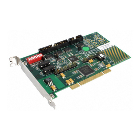
Ux is the location for the test device. Eight device boards are supplied with the INA2180-2181EVM board.
Each board is populated with one of the available device gains. This option enables users to test the
devices and determine the gain setting that is best suited for a given application.
The following is a list of the factors involved in selecting the appropriate device:
• The INA2180A1-A4 devices are identical with the exception of different gain settings. The INA2181A1-
A4 devices have the same device gain options of the INA2180 but with the addition of the reference
pin that enables bidirectional current measurements.
• Select INA2180 for unidirectional applications only, and select INA2181 for unidirectional or
bidirectional applications.
• The differential input voltage is applied across the inputs, or developed based on the load current that
flows through the shunt resistor.
• The limiting factor that requires attention to be given to device selection is the output voltage.
• The selected device must allow the output voltage to remain within the acceptable range after the
developed input voltage is amplified by the respective device gain. The output voltage must remain
within the range of 10 mV above ground to 100 mV below the supply voltage.
• An output below the minimum allowable output requires the selection of a device with a higher gain.
Likewise, an output above the maximum allowable output requires the selection of a device with a
lower gain.
4.4 Voltages Inputs (IN+1, IN–1, IN+2, IN–2)
The IN+1 (IN+2 for Channel 2) and IN–1 (IN-2 for Channel 2) inputs accept a differential voltage that is
amplified by the selected device gain and is presented at the OUT1 (OUT2 for Channel 2) test point.
These inputs can also be used to connect the differential voltage developed across an external shunt in an
existing circuit. The acceptable differential input voltage range and polarity are determined by the supply
voltage, reference voltage, and gain of the selected device.
4.5 Reference Voltage (REF1, REF2)
REF1 and REF2 test points enables the user to configure the INA2181A1-A4 device boards for either
unidirectional or bidirectional operation. Refer to Section 5 for more information.
4.6 Rx5 and Rx6
Rx5 and Rx6 resistors locations are not populated. If a 0-Ωresistor is populated, the REF1 (REF2 for
Channel 2) pin will be connected to GND, and the INA2181 can be used for unidirectional measurements.
These locations allow for 0805 surface-mount package size.
5 Reference Voltage Setup
The INA2181A1-A4 devices enable the use of an external reference. This reference determines how the
output responds to certain input conditions. The reference also enables these devices to be used in
unidirectional and bidirectional applications. The REF pin can also be connected to supply (VS) to enable
unidirectional measurement in the negative direction.
5.1 Unidirectional Mode
Unidirectional refers to a load current that flows in only one direction.
The INA2180A1-A4 devices are able to measure unidirectional currents only. The INA2181A1-A4 devices
measure unidirectional and bidirectional currents. For unidirectional measurements the REF pins (REF1
and REF2) needs to be connected to GND. You can connect the REF1 pin (REF2 for Channel 2) to GND
through a 0-ohm resistor (Rx5 and Rx6) or ground it directly.
